Note: Descriptions are shown in the official language in which they were submitted.
, 2037121
READ-OUT APPARATUS FOR SOLID STATE IMAGING DEVICE AND
IMAGE SCANNER USING THE SAME
The present invention relates to a read-out apparatus of a solid-
state imaging device and to an image scanner using the read-out apparatus.
A CCD (Charge-Coupled Device), which is an example of solid
state imaging devices used for image scanners, is provided with a large number
5 of sensor elements for converting light to electricity (named photoelectric
conversion) and for storing photoelectric charges obtained by the photoelectric
conversion, and with an analog shift register for transferring the charges stored
in the sensor elements and for successively outputting a voltage signal. The
voltage signal outputted from the analog shift register is sampled, and that
10 sample is converted into a digital signal.
In a CCD linear image sensor, sensor elements are disposed in
line. When a letter-sized (8.5-inch width) original is picked-up with a resolution
of 400 DPI (Dot Per Inch), the number of sensor elements, namely the number
of photoelectric converter elements, is 8.5 inches x 400 elements/inch = 3400
15 elements. However, the number of sensor elements in CCD linear image
sensors which are currently available and which meet applicable standards is
one of 1024, 2048, 2592, and 5000. Thus, to satisfy 3400 elements, it is
necessary to use a CCD linear image sensor with 5000 elements.
A conventional read-out apparatus is designed to scan all the
20 photoelectric converter elements of the CCD image sensor at a particular speed.
Thus, if image information inputted to the CCD linear image sensor with 5000
elements is read out with the conventional read-out apparatus, the photoelectricconverter elements which are not used for picking-up the image are also
scanned and unnecessary extra read-out time is thereby required. In other
25 words, in a case where an image of an original that can satisfactorily be picked-
up by a CCD sensor with 3400 elements is in fact picked-up by a CCD sensor
with 5000 elements, 1600 elements are unnecessarily read out, causing an
excess read-out time.
*
2û37121
Therefore, an object of the present invention is to provide, for use
with a solid state imaging device and an image scanner a read-out apparatus
that uses a shortened read-out time.
According to the present invention, the above-mentioned purpose
5 can be accomplished by a read-out apparatus for a solid state imaging device
having a plurality of photoelectric converter elements which convert an image
into photoelectric charges and store those photoelectric charges. The apparatus
includes a shift register means for sequentially shifting charges, transferred from
the photoelectric converter elements, to output image signals corresponding to
10 the photoelectric converter elements. It also includes a gate means for
sequentially transferring the charges stored in the photoelectric converter
elements to the shift register means each time a transfer signal is applied
thereto, and further includes a transfer signal generation means for generating
the transfer signal when an image signal corresponding to a predetermined one
15 of the photoelectric converter elements is outputted. With his arrangement,
charges in the shift register means from one transfer operation from the
photoelectric converter elements are partially overlapped with charges
transferred in a previous transfer operation.
Light that has entered into the solid state imaging device is stored
20 in the photoelectric converter elements as photoelectric charges. The stored
photoelectric charges are transferred, and then read out in succession. Reading
out a photoelectric charge corresponding to a predetermined one of the
photoelectric converter elements in one scanning cycle prompts the read-out
operation of the subsequent scanning cycle to start; meanwhile, the current
25 scanning cycle continues. Thus, charges of those photoelectric converter
elements which are not used for picking-up an original image in a scanning
cycle, as well as charges of those photoelectric converter elements used for
picking-up the original image in the subsequent scanning cycle, can be read out
simultaneously. Thus, the read-out time for the simultaneous read-out operation
30 can be reduced. Consequently, the read-out speed of the solid state imaging
device can be remarkably increased by this simple arrangement.
3 2037121
It is preferable that the shift register means shifts the transferred
charges at a constant speed. It is also preferable that the read-out apparatus
includes a clock pulse generation means for generating clock pulses used for
shifting the transferred charges in the shift register means. Preferably, the clock
5 pulse generation means generates clock pulses with a constant frequency so
that the shift register means shifts the transferred charges at a constant speed.
It is further preferable that the clock pulse generation means has a pulse
generator for generating clock pulses, and has a counter for counting the clock
pulses from the pulse generator to produce frequency-divided pulses.
The transfer signal generation means may preferably have a pulse
generator for generating clock pulses, and have a counter for counting the clockpulses from the pulse generator to produce a carry output when the counter
counts a predetermined number of the clock pulses. The transfer signal
generation means may preferably further include a flip-flop circuit for generating
15 pulses having a predetermined pulse width in response to the carry output from
the counter.
The shift register means may alternately shift the transferred
charges at two different constant speeds. In that case, the clock pulse
generation means may generate two kinds of clock pulses each with a different
20 constant frequency, so that the shift register means shifts the transferred
charges at two different constant speeds. The clock pulse generation means
includes a pulse generator for generating two kinds of clock pulses with different
constant frequencies, and a counter for selectively counting one of the two kinds
of clock pulses from the pulse generator to produce frequency-divided pulses.
25 It is preferable that the clock pulse generation means includes a circuit forapplying pulses having the higher frequency to the counter when the image
signals corresponding to the charges overlapped with charges transferred in a
previous transfer operation are outputted, and for applying pulses having the
lower frequency to the counter when the image signals corresponding to the
30 charges not overlapped with charges transferred in a previous transfer operation
are outputted.
2~371~1
According to the present invention, the purpose can be
accomplished by an image scanner including: a solid state imaging device
having a plurality of photoelectric converter elements which convert image into
photoelectric charges and store the photoelectric charges, a shift register means
for sequentially shifting charges transferred from the photoelectric converter
elements to output image signals which correspond to the photoelectric
converter elements, and a gate means for transferring the charge stored in the
respective photoelectric converter elements to the shift register means each
time a transfer signal is applied thereto. A transfer signal generation means
generates the transfer signal when an image signal corresponding to a
predetermined one of the photoelectric converter elements is outputted, so that
charges in the shift register means transferred from the photoelectric converterelements are partially overlapped with charges transferred in a previous transfer
operation.
Further objects and advantages of the present invention will be
apparent from the following description of the preferred embodiments of the
invention as illustrated in the accompanying drawings, in which:
Figure 1 is a schematic block diagram of an image scanner of a
preferred embodiment of the present invention;
Figure 2 is a schematic side view of an optical system for the
image scanner of Figure 1;
Figure 3 is a schematic block diagram of the CCD image sensor
of the embodiment of Figure 1;
Figure 4 is an electrical schematic drawing of a sample hold circuit
of the embodiment of Figure 1;
Figure 5 is a schematic block diagram of a signal generator
included in a controller of Figure 1;
Figure 6 is a timing chart of each signal of the circuit of Figure 5;
Figure 7 is a timing chart of some of the signals of Figure 1,
illustrating how a CCD output voltage is controlled;
- 2037121
Figure 8 is a schematic block circuit diagram of a signal generator
of another embodiment of the present invention;
Figure 9 is a timing chart of some of the signals of the block circuit
diagram of Figure 8; and,
Figure 10 is a timing chart of some of the signals controlling a
CCD output voltage in the embodiment of Figure 8.
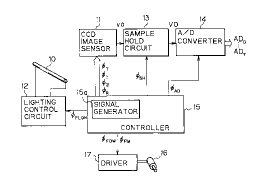
Figure 1 is a schematic drawing showing the construction of an
image scanner of a preferred embodiment of the present invention. In the
image scanner, an image of an original illuminated by a light source of a
fluorescent lamp 10 is picked-up by a CCD image sensor 11. The CCD image
sensor 11 is a CCD linear image sensor in which a large number of sensor
elements are aligned. In the present embodiment, an image which can be
satisfactorily picked-up by a CCD image sensor with 3400 elements is picked-up
by using the CCD image sensor 11 with 5000 elements. The horizontal
scanning operation of the image scanner is electrically conducted by applying
clock pulses to the CCD image sensor 11. In contrast, the vertical scanning
operation of the image scanner is mechanically conducted by moving the
original image.
As shown in Figure 1, the fluorescent lamp 10 is connected to a
lighting control circuit 12 for controlling turn on and turn off of the fluorescent
lamp 10. An optical system is constituted so that the light from the fluorescentlamp 10 is applied to the original, and reflected light from the original is applied
to the CCD image sensor 11. The output terminal of the CCD image sensor 11
is coupled with the input terminal of an A/D converter 14 through a sample hold
circuit 13. The A/D converter 14 outputs an 8-bits digital image signal ADo-
AD7.
The lighting control circuit 12, the CCD image sensor 11, the
sample hold circuit 13, and the A/D converter 14 are connected to a controller
15 which is preferably formed by a microprocessor, and are controlled by pulse
signals sent from the controller 15. The controller 15 is provided with a signalgenerator 1 5a for generating a part of these pulse signals. The controller 15 is
- 2037121
also connected to a driver 17 of a pulse motor 16 for mechanically moving the
original for vertical scanning.
The lighting control circuit 12 turns on and off the fluorescent lamp
10 when a signal 0FLON sent from the controller 15 is set to "1" and "0",
5 respectively.
Figure 2 is a schematic side view of the optical system of the
embodiment shown in Figure 1.
As shown in Figure 2, a glass table 20 and the original 21 placed
thereon are moved in the directions shown by arrows A and B by means of the
pulse motor 16 shown in Figure 1. Thus, the original 21 is vertically scanned.
The light from the fluorescent lamp 10, which is extending in the horizontal
scanning direction perpendicular to the vertical scanning direction, is applied to
the original 21 through the glass table 20. The light 22 reflected by the original
21 enters on the light-receiving surface of the CCD image sensor 11, after
15 passing through the glass table 20 again, and being reflected by a mirror 23
through a lens 24. As aforementioned, the CCD image sensor 11 is composed
of a large number of sensor elements aligned in the horizontal scanning
direction so as to receive the reflected light.
The driver 17 shown in Figure 1 drives the pulse motor 16 in
20 accordance with a direction control signal 0FOW and a step-feed signal 0PM sent
from the controller 15. When the direction control signal 0FOW jS set to "0", the
glass table 20 moves in the direction of, for example, the arrow A in accordancewith the number of pulses of the step-feed signal 0PM When the direction
control signal 0FOW jS set to "1", the glass table 20 moves in the direction of the
25 arrow B in accordance with the number of pulses of the step-feed signal 0PM
It is possible to move the glass table 20 by using a DC motor
instead of the pulse motor. Although, in the present embodiment, the vertical
scanning operation is conducted by moving the glass table 20 and also the
original 21, it is possible to alternately conduct the vertical scanning operation
30 by mechanically moving the fluorescent lamp 10 and the optical system for
guiding the light reflected from the original 21 to the CCD image sensor 11.
20371~ 1
Figure 3 is a schematic drawing showing the electrical construction
of the CCD image sensor 11 of the embodiment shown in Figure 1. The CCD
image sensor 11 is composed mainly of a large number of sensor elements, for
example, 5000 elements S1 - S5000, aligned in the horizontal scanning direction
for conducting photoelectric conversion and for storing photoelectric charges
obtained by the photoelectric conversion, and a large number of analog shift
registers, for example, 5000 registers SR1 - SR5000, connected to the respectivesensor elements S1 - S5000 through a transfer gate 30. An output terminal of theanalog shift registers SR' - SR5000 is connected to an output buffer 31.
10When a transfer pulse 0TjS sent from the controller 15 (Figure 1 )
to the transfer gate 30, the photoelectric charges stored in the sensor elementsS, - S5000 are simultaneously transferred to the analog shift registers SR1 -
SR5000, respectively. The charges transferred to the respective analog shift
registers SR, - SR5000 are successively transferred to the output buffer 31 in
15synchronization with clock pulses 0, and 02 sent from the controller 15. The
charges fed to the output buffer 31 are outputted as a CCD output voltage vo.
Reset pulses 0R are sent from the controller 15 to the output buffer 31 so as toreset the output buffer 31.
The CCD output voltage vo is applied to the sample hold circuit 13,
wherein the applied CCD output voltage vo is sampled and compensated to
produce an analog voltage VO.
Figure 4 is an electrical schematic drawing of the construction of
the sample hold circuit 13. This sample hold circuit 13 serves to sample an
image signal inputted thereto, and to compensate the DC component of the
sampled image signal.
In the circuit of Figure 4, the inputted CCD output voltage vo is
applied to an input terminal of a MOS (Metal Oxide Semiconductor) transistor
40, which is an example of an analog switch. To a gate of the MOS transistor
40, sample hold pulses 0SH are applied. An output terminal of the MOS
30 transistor 40 is connected to a clamping circuit through a voltage follower 41
and a capacitor 42. The clamping circuit includes a voltage follower 43 and a
20~7121
MOS transistor 44. To a terminal of this MOS transistor 44 a DC voltage, for
example, +4 V, is applied. To a gate of the MOS transistor 44, clamping pulses
0CLAMP are applied. Generally, since the CCD image sensor is DC coupled with
the subsequent circuit, the DC component of the image signal (which is mainly
5 the background portion of the image) is lost. Therefore, it is necessary to add
the lost DC component after the image signal is amplified to a required level.
The addition of the lost DC component, namely through compensation of the DC
level, is conducted by the clamping circuit. The analog voltage, VO where the
DC level has been compensated, is outputted from the voltage follower 43.
The above analog switch may be formed by using bipolar
transistors or diodes instead of the MOS transistors 40 and 44.
The analog voltage VO from the sample hold circuit 13 is applied
to an A/D converter 14. In the A/D converter 14, the analog voltage VO is
converted into an 8-bit digital image signal ADo - AD7 in accordance with an A/D15 conversion pulse 0AD- The A/D converter 14 converts an analog signal voltage,for example, of +2 V to +4 V, into an 8-bit (256-level) digital signal. Thus, when
the CCD output voltage vo sent from the CCD image sensor 11 is +4 V (in a
black level, namely, a voltage level where light is not applied), each bit of the
output signal ADo - AD7 sent from the A/D converter 14 becomes "0". In
20 contrast, when the CCD output voltage vo is +2 V (in a white level, namely
saturated voltage level where light is applied), each bit of the output signal ADo ~
AD7 sent from the A/D converter becomes "1".
Figure 5 is a circuit schematic drawing of a signal generator 15a
of the controller 15 shown in Figure 1. The signal generator 15a is a circuit for
25 generating some of the pulse signals, such as the transfer pulses 0T. the clock
pulses 01 and 02- and the reset pulses 0R-
As shown in Figure 5, the signal generator 15a is provided with agenerator 50 for generating basic clock pulses 0t whose frequency is for
example 2 MHz. Although the generator 50 uses a crystal oscillator, it is
30 possible to construct the generator 50 by using a PLL (Phased-Locked Loop)
circuit or the like. An output terminal of the generator 50 is connected to a
9 2037121
pulse input terminal T of a counter 51, an input terminal of a three-input AND
gate 52, and, through an inverter 53, an input terminal of a three-input NAND
gate 54. An output terminal QA f the counter 51 is connected to an input
terminal of the AND gate 52 and an input terminal of the NAND gate 54. An
output terminal QB Of the counter 51 is connected to an input terminal of the
inverter 55. An output signal of the output terminal QB jS used as the clock
pulses 01. The clock pulses 0, are inverted by the inverter 55, and then used
as the clock pulses 02. An output terminal of the inverter 55 is connected to aninput terminal of the AND gate 52 and an input terminal of the NAND gate 54.
A carry output terminal CA of the counter 51 is connected to a clock input
terminal T of a D flip-flop 57 through an inverter 56.
Signals outputted from an output terminal of the AND gate 52 are
the reset pulses 0R Signals outputted from an output terminal of the NAND
gate 54, designated RESET signals, are applied to a reset input terminal R of
the D flip-flop 57. An input terminal D of the flip-flop 57 is pulled up to +5 V.
Signals outputted from an output terminal Q of the flip-flop 57 are the transferpulses 0T-
Figure 6 is a timing chart of each signal of the circuit shown in
Figure 5. The basic clock pulses 0t whose frequency is 2 MHz are generated
by the generator 50 and sent to the counter 51. Thus, a 1-MHz output signal
QA obtained by dividing the frequency of the basic clock pulses by 2 is producedfrom the output terminal QA Of the counter 51, and a 500-KHz output signal QB
obtained by dividing the frequency of the basic clock pulses by 4 is produced
from the output terminal QB. The output signal QB jS used as the clock pulses
0~. The clock pulses 02 are obtained by inverting the clock pulses 01.
The basic clock pulses 0t from the generator 50, the clock pulses
02~ and the output signal QA Of the counter 51 are ANDed by the AND gate 52,
and the reset pulses 0R are thereby obtained. In addition, the pulses obtained
by inverting the basis clock pulses 0t from the generator 50, the clock pulses
02~ and the output signal QA Of the counter 51 are inversely ANDed by the
- 2~371~1
and the RESET signals are thereby obtained. In Figure 6, the RESET signal is
the inversion of the RESET signal.
When the counter 51 counts 8400 times the basic clock pulses 0t
applied to the input terminal T, a carry output signal CARRY is generated in
synchronization with the rising edge of the 8400th pulse 0t. The carry output
signal CARRY is applied to the clock input terminal T of the D flip-flop 57
through the inverter 56. Thus, when the level of the carry output signal CARRY
falls, the transfer pulse 0T jS outputted from the output terminal Q of the D flip-
flop 57. The RESET pulse causes the transfer pulse 0T to fall.
Figure 7 is a timing chart of some of the signals of Figure 1,
illustrating how CCD output voltage vo from the CCD image sensor is controlled
by the aforementioned transfer pulses 0T, the clock pulses 0, and 02~ and the
reset pulses 0R-
When the transfer pulses 0T are sent from the signal generator
15a (see Figure 1) to the transfer gate 30 of the CCD image sensor 11 (see
Figure 3), the photoelectric charges stored in the 5000 sensor elements S, -
S5000 are transferred to the 5000 analog shift registers SR, - SR5000 in
accordance with a first transfer pulse 0T1. Thus, the charges are read out and
thereby the CCD output voltages vo, - vo5000 sent from the 5000 sensor
elements S, - S5000 are outputted successively to the output buffer 31 in
synchronization with the clock pulses 0, and 02 Each of the CCD output
voltages vo, - vo5000 outputted to the output buffer 31 is reset every time the
reset pulse 0R jS applied.
When the 8400th basic clock pulse 0t sent from the generator 50,
namely the 2100th clock pulse 0, (which is equivalent to the 4200th clock pulse
where the clock pulses 0, and 02 are added), is applied to the CCD image
sensor 11, a second transfer pulse 0T2 jS applied to the transfer gate 30 of theCCD image sensor 11. Thus, the charge stored in the sensor element S4201 of
the CCD image sensor 11 is added to the charge stored, after the previous
charge-transferring operation, in the sensor element S,. The result of this
addition is outputted as the CCD output voltage vo,. Accordingly, as shown in
2037121
11
Figure 7, the voltages corresponding to the sum of the charges stored in the
sensor elements S420, - S5000 and the charges stored in the sensor elements
S, - S800 in the subsequent cycle, respectively, are outputted from the output
buffer 31 as the CCD output voltages vo, - vo800. As described above, in the
present embodiment, since the original image capable of being picked-up by
using the CCD image sensor with 3400 elements is picked-up by the CCD
image sensor 11 with 5000 elements, the 1st to 800th sensor elements and the
4201st to 5000th sensor elements are not used for picking-up the original
image. Only the 801st to 4200th sensor elements are used for picking-up the
original image. Thus, by controlling the circuit in the aforementioned manner,
only the CCD output voltages VO80~ - VO4200 from the CCD image sensor 11 are
used as the image signal.
The obtained CCD output voltages vo80, - vo4200 are sampled by
the sample hold pulses 0SH and compensated in the DC level by the clamping
pulses 0CLAMP in the sample hold circuit 13. The resultant signals are sent to
the A/D converter 14 and then converted into digital signals in synchronization
with the AD pulses 0AD
According to the present embodiment, if the frequency of the basic
clock pulses 0t jS 2 MHz, one scanning cycle becomes 4.2 msec and thereby
the scanning time of the present embodiment becomes shorter than that of the
related art by 0.8 msec.
In addition, by changing the counting times of the counter 51 from
4800 to 4400 so as to shorten the period of the transfer pulse, the 801st to
4200th output voltages vo80, - vo4200 can be continuously outputted.
Figure 8 is a schematic drawing showing the circuit construction
of a signal generator of another embodiment in accordance with the present
invention. The overall construction of this embodiment is the same as that
shown in Figure 1. The difference between this embodiment and that shown in
Figure 1 is that the read-out pulse period of the charges stored in the sensor
elements S, - S800, which are not used for the image picking-up operation of theCCD image sensor 11, is half the read-out pulse period of the sensor elements
,~ ,
-
12 2037121
S80, - S4200, which are used for the image picking-up operation thereof, namely
2 MHz.
As shown in Figure 8, a signal generator used in this embodiment
is provided with a generator 80 for outputting two basic clock pulses 0t1 and 0t2
with two different frequencies, for example, 4 MHz and 2 MHz, respectively.
The generator 80 may use two different crystal oscillators for generating such
different frequency pulses or use different PLLs for that. Of course, it is
possible to multiply the frequency of the pulses from one crystal oscillator.
Two output terminals of the generator 80 are connected to input
terminals A and B of a data selector 81, respectively. The data selector 81 is
constructed as follows. When a HSD signal (high-speed signal) applied to a
control input terminal SELECT is set to "1", the input terminal A is connected to
an output terminal OUT, and thereby the basic clock pulses 0t1 are outputted.
On the other hand, when the HSD signal is set to "0", the input terminal B is
connected to the output terminal OUT, and thereby the basic clock pulses 0t2
are outputted.
An output terminal for the basic clock pulses 0t1 Of the generator
80 is also connected to a pulse input terminal T2 of a counter 82. An output
terminal OUT of the data selector 81 is connected to a pulse input terminal T1
of a counter 83, an input terminal of a three-input AND gate 84, and, through
an inverter 85, an input terminal of a three-input NAND gate 86. An output
terminal QA1 Of the counter 83 is connected to an input terminal of the AND gate84 and an input terminal of the NAND gate 86. An output terminal QB1 Of the
counter 83 is connected to an input terminal of an inverter 87. An output signalof the output terminal QB1 jS used as clock pulses 01. The clock pulses 01 are
inverted by the inverter 87 to be used as the clock pulses 02. An output
terminal of the inverter 87 is connected to an input terminal of the AND gate 84and an input terminal of the NAND gate 86. A carry output terminal CA1 of the
counter 83 is connected to a clock input terminal T, of a D flip-flop 89 throughan inverter 88. The carry output terminal CA, is also connected to a clock inputterminal T2 of a D flip-flop 90.
,
13 2037121
Signals outputted from an output terminal of the AND gate 84 are
used as reset pulses 0R Signals outputted from an output terminal of the
NAND gate 86, designated RESET signals, are applied to a reset input terminal
R, of the D flip-flop 89. An input terminal D, of the flip-flop 89 is pulled up to
+5 V. Signals outputted from an output terminal Q~ of the flip-flop 89 are used
as transfer pulses 0T-
A carry output terminal CA2 of the counter 82 is connected to a
reset input terminal R2 of the D flip-flop 90 through an inverter 91. To a resetinput terminal R of the counter 82, an inverted transfer pulse 0T outputted froman inverted output terminal Q~ of the D flip-flop 89 is applied. An input terminal
D2 of the D flip-flop 90 is pulled up to +5 V. The HSD signal is outputted from
an output terminal Q2 Of the D flip-flop 90.
Figure 9 is a timing chart of each signal of the circuit shown in
Figure 8. The 4 MHz basic clock pulses 0t1 and the 2 MHz clock pulses 0t2 are
outputted from the generator 80 to the input terminals A and B of the data
selector 81, respectively.
When the HSD signal is set to "0", the data selector 81 outputs the
2-MHz basic clock pulses 0t2. Thus, 1-MHz output signal QA~ obtained by
dividing the frequency of the 2-MHz basic clock pulses 0t2 by 2 is produced
from the output terminal QA~ of the counter 83, and 500-KHz output signal QB2
obtained by dividing the frequency of the 2-MHz basic clock pulses 0t2 by 4 is
produced from the output terminal QB2 Of the counter 83. The output signal QB2
is outputted as clock pulses 0,. The clock pulses 02 are pulses obtained by
inverting the clock pulses 0,.
The basic clock pulses 0t2~ the clock pulses 02 inverted, and the
output signal QA~ of the counter 83 are ANDed by the AND gate 84 and reset
pulses 0R are thereby obtained. In addition, the pulses obtained by inverting
the basic clock pulses 0t2~ inverting the clock pulses 02~ and using the output
signal QA~ of the counter 83 are inversely ANDed by the NAND gate 86, and
RESET pulses are thereby produced. In Figure 9, the RESET signal is the
inversion of the RESET signal.
14 2037121
When the counter 83 counts 8400 times the basic clock pulses 0t2
applied to the input terminal T" one carry output signal CARRY1 is generated
in synchronization with the rising edge of the 8400th pulse. The carry output
signal CARRY1 is applied to the clock input terminal T, of the D flip-flop 89
5 through the inverter 88. Thus, when the level of the carry output signal
CARRY1 falls, the transfer pulse 0T jS outputted from the output terminal Q~ of
the D flip-flop 89. The RESET pulses cause the transfer pulse 0T to fall. The
carry output signal CARRY1 is also applied to the clock input terminal T2 of theother D flip-flop 90, and thereby the level of the HSD signal, which is the output
signal of the output terminal Q2. changes from "0" to "1". Thus, the data
selector 81 is switched so that the 4-MHz basic clock pulse 0t1 iS outputted.
To the input terminal T2 of the counter 82, the basic clock pulses
0~1 are always applied. The pulses 0T. obtained by inverting the transfer pulses0T. are applied to the reset input terminal R of the counter 82 so as to cause
the counter 82 to synchronize with the counter 83. When the inverted transfer
pulse 0T jS applied to the reset terminal R of the counter 82, the counter 82 isreset. When the basic clock pulses 0t1 are applied to the input terminal T2 799
times, the counter 82 generates one carry output signal CARRY2 in
synchronization with the rising edge of the 799th pulse 0t1- The carry output
signal CARRY2 is applied to the reset input terminal R2 of the D flip-flop 90
through the inverter 91. Thus, the D flip-flop 90 is reset, and thereby the level
of the HSD signal from the output terminal Q2 changes from "1" to "0".
Consequently, the data selector 81 is switched so that the 2-MHz basic clock
pulses 0t2 are outputted.
As described above, while the charges stored in the sensor
elements S80, - S4200 used for the image picking-up operation of the CCD image
sensor 11 are read out, the 2-MHz basic clock pulses 0t2 are used. On the
other hand, while the charges stored in the sensor elements S, - S800 and S420, -
S5000, which are not used for the image picking-up operation, are read out, the
data selector 81 is switched so as to use the 4-MHz basic clock pulses 0t1-
Thus, each read-out period of the sensor elements S, - S800 and S420, - S5000,
15 2037121
which are not used for the image picking-up operation, is half as long as the
read-out period of the sensor elements S801 - S4200, which are used for the image
picking-up operation, thereby reducing the read-out time. Moreover, for the
sensor elements S, - S800 and S4201 - S5000, a read-out error thereof does not
affect the image picking-up operation of the CCD image sensor 11. It is
possible to use clock pulses whose frequency is higher than 2 MHz.
Figure 10 is a timing chart of each signal describing how CCD
output voltage vo is controlled by the aforementioned transfer pulses 0T~ the
clock pulses 01 and 02~ and the reset pulses 0R-
When the transfer pulse 0T jS applied from the signal generator to
the transfer gate 30 of the CCD image sensor 11 (see Figure 3), the charges
stored in the sensor elements S1 - S5000 are transferred to the 5000 respective
analog shift registers SR, - SR5000 in synchronization with a first transfer pulse
0T1 Thus, the charges are read out and then the CCD output voltages vo, -
VO5000 are successively outputted from the 5000 sensor elements S, - S5000 to the
output buffer 31. Each of the CCD output voltages vo, - vo5000 outputted to the
output buffer 31 is reset every time the reset pulse 0R jS applied.
When the 8400th basic clock pulses 0t1 and 0t2~ namely the
2100th clock pulse 0, (which is equivalent to the 4200th clock pulse where the
clock pulses 0, and 02 are added), are applied to the CCD image sensor 11,
a second transfer pulse 0T2 iS applied to the transfer gate 30 of the CCD image
sensor 11. Therefore, the charges stored in the sensor element S420, of the
CCD image sensor 11 is added to the charge stored, after the previous charge-
transferring operation, in the sensor element S1. The result of this addition isoutputted as the CCD output voltage vo,. Accordingly, as shown in Figure 10,
the voltages corresponding to the sum of the charges stored in the sensor
elements S4201 - S5000 and the charges stored in the sensor elements S1 - S800
in the subsequent cycle, respectively, are outputted from the output buffer 30
as the CCD output voltages vo, - vo800.
During the read-out operation of the CCD output voltages vo, -
vo800, which are not used for the image picking-up operation, the 4-MHz basic
.~
2037121
16
clock pulses 0t, are used as described above. Thus, the read-out period of the
voltages which are not used for the image picking-up operation becomes half
as much as the read-out period of the voltages which are used for the image
picking-up operation, thereby remarkably reducing the read-out time.
As described above, according to this embodiment, the charges
of the 1st to 800th sensor elements of the CCD image sensor 11 and the
charge of the 4201st to 5000 sensor elements are read out simultaneously in
half the time of the read-out operation of sensor elements used for the image
picking-up operation. Therefore, one period of the transfer pulses 0T becomes
0.3 msec + 3.4 msec = 3.7 msec. Consequently, the read-out period can be
reduced by approximately 1.3 msec in comparison with the related art.
In the aforementioned embodiments, the CCD image sensor with
5000 sensor elements was used. However, the present invention can be
applied to other solid state imaging devices with a different number of sensor
elements. Moreover, the present invention can be applied to originals in other
than the letter size.
Furthermore, even if the number of sensor elements required is not
fixed, the present invention can be applied for changing the number of pulses
generated by the counter. In addition, the original image can be read out in a
shorter time proportional to the number of sensor elements.
The read-out apparatus of the solid state imaging device according
to the present invention can be applied to an image-forming apparatus such as
a copy machine and a facsimile machine, as well as the image scanner.
Many widely different embodiments of the present invention may
be constructed without departing from the spirit and scope of the present
invention. It should be understood that the present invention is not limited to the
specific embodiments described in the specification, except as defined in the
appended claims.