Note: Descriptions are shown in the official language in which they were submitted.
~~~W~~
APPARATUS AND METHOD FOR CAhIBRi.ATION IN A UPECTROPHOTOMETER
BACKGROUND OF THE INVENTION
Field of the Invention.
The invention relates to apparatus and methods associated
with color measurement and analysis technology and, more
particularly, apparatus and methods for compensating color
measurement parameters for changes in light source temperature
and intensities, and for also compensating such measurements with
respect to spectral filter characteristics and the like.
Description of Related Art.
It is well-known that the term "color" as applied to
electromagnetic radiation represents in part the relative energy
distribution of radiation within the visible spectrum. That is,
light providing a stimulus to the human eye, and having a
particular energy distribution, may be perceived as a
substantially different color than light of another energy
distribution. Concepts relating to the characteristics of color
and light waves are the subject of numerous well-known texts,
such as Principles of Color Technology, Meyer, Jr. and Saltzman
(Wiley 1966) and The Measurement of Appearance, Hunter and Harold
(Wiley 2nd Ed. 1987).
In recent years, the capability of maintaining the "quality
of color" has been of significant importance in various
industries, such as, for example, the fields of graphic arts,
photography and color film processing. For purposes of
performing sample testing and other activities in furtherance of
maintaining color quality, it is necessary to first determine an
appropriate means for "measuring" and "describing" color. A
substantial amount of research has been performed during the past
50 years with respect to appropriate methods and standards for
color measurement and description.
-1-
For purposes of describing color, and from a purely
"physical" point of view, the production of color requires three
things: a source of light; an object to be illuminated; and, a
means for perceiving the color of the object. The means for
perceiving the color can be the human eye and brain or,
alternatively, electrical and electromechanical apparatus such as
photosensitive detectors and associated auxiliary devices
utilized for detecting light. In general, it is desirable to
provide a means for measuring color so as to assess the manner in
l0 which an image will appear to a human observer, or the manner in
which an image will perform in a photographic or other type of
reproduction printing operation.
Although human perception and interpretation of color can be
useful, reliance on such perception and interpretation can be
highly subjective. That is, human nature may cause one person's
perception of the color of a particular object to be
substantially different from the perception of another. In
addition, eye fatigue, age and other physiological factors can
influence color perception. Further, visual human perception is
often insufficient for color description. For example, certain
object samples may be visually perceived under one light source
as substantially "matching", and yet may actually have very
different spectral characteristics and may be perceived as "non-
matching" under another light source. In view of the foregoing,
it is desirable to employ color measurement and description
techniques which are objective in nature, and capable of
differentiating among object samples having different color
characteristics.
Various devices have been developed and are widely utilized
to measure and quantitatively describe color characteristics of
object samples. Many of these devices provide measurements
related to the spectral characteristics of the samples.
Described simplistically, when light is directed onto an object
sample to be measured for color, the object may absorb a portion
-2-
'l ~~~
~d ~..~ f3 ~ ~ c
of the light energy, while correspondingly passing through or
reflecting (if the object is opaque) other portions of the light.
The color characteristics of the object sample will depend in
part on the spectral characteristics of the object. That is, the
effect of an object on light can be described by its spectral
transmittance or reflectance curves (for transparent or opaque
materials, respectively). These spectral characteristic curves
indicate the fraction of the source light at each wavelength
transmitted by or reflected from the materials. Such curves are
a means for describing the effect of an object on light in a
manner similar to the use of a spectral energy distribution curve
for describing the characteristics of a source of light.
Instruments utilized for generating such spectral characteristics
curves are typically referred to as spectrophotometers.
Although the present invention is disclosed with respect to
use in a spectrophotometer, it is worthwhile, for purposes of
background, to describe the use of other color measurement
devices. In particular, for purposes of background description
of typical types of components employed in many color measurement
devices, concepts associated with a reflectance densitometer are
set forth in the following paragraphs.
In accordance with conventional optical physics, its is
known, that the proportion of light incident to an object sample
and absorbed by such a sample is independent of the light
intensity. Accordingly, a quantitative indication of the
spectral characteristics of an object sample can be defined as
the "transmittance" or "reflectance" of the sample. That is, the
transmittance of a substantially transparent object can be
defined as the ratio of power transmitted over light power
incident to the sample. Correspondingly, for an opaque object
sample, the reflectance can be defined as the ratio of power
reflected from the object over the incident light power.
For collimated light, these ratios can be expressed in terms
of intensities, rather than power. Furthermore, because of the
-3-
4'r !1 't'') '' '.i %t
f~ ~ c) ~ c~ :~a a.
nature of transmittance/reflectance and the optical
characteristics of the human eye, it is sometimes advantageous to
express these ratios in logarithmic: form. Accordingly, one
parameter widely used in color technology fields for obtaining a
quantitative measurement or "figure of merit" is typically
characterized as optical "density.'° The optical density of an
object sample is typically defined as follows:
Optical Density = D = -logo T or -logo R (Equation 1)
where T represents transmittance of a transparent object and R
represents reflectance of an opaque object. In accordance with
the foregoing, if an object sample absorbed 90% of the light
incident upon the sample, and the object were opaque, the
reflectance would ideally be 10%. The density of such a sample
would then be characterized as unity. Correspondingly, if 99.9%
of the light were absorbed, the reflectance would be 0.1% and the
density would be 3. Similarly, the density of an "ideal" object
reflecting 100% of the light incident upon the object would be 0.
To provide a relative measurement of color, it is possible
to utilize the principles of optical density, without requiring
measurement or knowledge of the absolute values of total incident
light intensity or reflectance. That is, for example, it is
possible to obtain relative color measurements among a series of
object samples by utilizing a particular geometric configuration
of light, object sample and reflectance or transmittance detector
for each measurement, and standardizing the measurements in some
desired manner.
In brief summary, optical density is a measurement of the
modulation of light or other radiant flux by an object sample,
such as a given area of a photographic print. Density
measurements provide a means to assess the manner in which an
image will appear to a human observer, or the way an image will
perform in a film processing operation. Density measurements can
-4-
be utilized to produce sensitometric curves to evaluate various
printing and reproduction characteristics, as well as utilization
to control various photographic operations, such as film
processing.
For purposes of measuring optical densities, it is well-
known to employ a device typically characterized as a
"densitometer." These densitometers are often categorized as
either "reflection" densitometers, employed for optical density
measurements of opaque objects, or are otherwise characterized as
"transmittance" densitometers. Transmittance densitometers are
employed for determining spectral characteristics of various non-
opaque materials.
FIG. 1 illustrates a simplified schematic representation of
a known reflection densitometer configuration 100. A
configuration of this type is described in detail in the commonly
assigned U.S. Patent Application Serial No. 105,424 filed October
5, 1987. Densitometer apparatus of the type shown in FIG. 1 are
characterized as reflection densitometers, and utilized to
provide color density measurements of opaque materials as
previously described.
Referring specifically to FIG. 1, and to numerical
references therein, the densitometer apparatus 100 includes a
light.source unit 102 having a source light 104. With respect to
optical density measurements in photography, color film
processing, and other industrial fields, various standards have
been developed for densitometer light source illuminants. For
example, densitometer light source standards have previously been
described in terms of a tungsten lamp providing an influx from a
lamp operating at a Planckian distribution of 3000° K. Other
suggested standards have been developed by the American National
Standards Institute ("ANSI") and the International Organization
for Standardization ("ISO"). These source light densitometer
standards are typically defined in terms of the spectral energy
distribution of the illuminant. The source light 104 preferably
-5-
G'j 4 ' ~ 1 ' i ' > -i
l,~ ij e~ ,~ t) ~r ~r~
conforms to an appropriate standard and can, for example,
comprise a filament bulb meeting a standard conventionally known
in the industry as 2856K ANSI. Power for the source light 104
and other elements of the densitometer apparatus 100 can be
provided by means of conventional rechargeable batteries or,
alternatively, interconnection to AC utility power.
The source light 104 projects light through a collimating
lens 106 which serves to focus the electromagnetic radiation from
the source light 104 into a narrow collimated beam of light rays.
Various types of conventional and well-known collimating lenses
can be employed. The light rays transmitted through the
collimating lens 106 project through an aperture 108. The
dimensions of the aperture 108 will determine the size of the
irradiated area of the object sample under test.
Various standards have been defined for preferable sizes of
the irradiated area. Ideally, the aperture 108 is of a size such
that the irradiance is uniform over the entire irradiated area.
However, in any physically realizable densitometer arrangement,
such uniform irradiance cannot be achieved. Current standards
suggest that the size of the irradiated area should be such that
irradiance measured at any point within the area is at least 90%
of the maximum value. In addition, however, aperture size is
typically limited to the size of the color bar or color patch
area to be measured, and is also sized so as to reduce stray
light.
The light rays emerging from the aperture 108 (illustrated
as rays 110 in FIG. 1) are projected onto the irradiated area
surface of an object sample 112 under test. The sample 112 may
be any of numerous types of colored opaque materials. For
example, in the printing industry, the sample 112 may be an ink-
on-paper sample comprising a portion of a color bar at the edge
of a color printing sheet. Further, with respect to the
illustrative embodiment of a densitometer apparatus employing the
principles of the invention as described in subsequent paragraphs
-6-
'": a,"~ k 1 ~~ " i ~/~ ;'i
!~ C,: C.~ F,s ~~~
herein, the sample 112 may be a control strip employed in the
color film processing industry.
As the light rays 110 are projected onto the object sample
112, electromagnetic radiation shown as light rays 114 will be
reflected from the sample 112. Standard detection configurations
have been developed, whereby reflected light is detected at a
specific angle relative to the illumination light rays 110
projected normal to the plane of the object sample 112. More
specifically, standards have been developed for detection of
reflected light rays at an angle of 45° to the normal direction
of the light rays 110. This angle of 45° has become a standard
for reflectance measurements, and is considered desirable in that
this configuration will tend to maximize the density range of the
measurements. In addition, however, the 45° differential also
represents somewhat of a relatively normal viewing configuration
of a human observer (i.e. illumination at a 45° angle from the
viewer's line of sight).
For purposes of providing light detection, a spectral filter
apparatus 116 is provided. The filter apparatus 116 can include
a series of filters 118, 120 and 122. The filters 118, 120 and
122 are employed for purposes of discriminating the cyan, magenta
and yellow spectral responses, respectively. That is, each of
the filters will tend to absorb light energy at frequencies
outside of the bandwidth representative of the particular color
hue of the filter. For example, the cyan filter 118 will tend to
absorb all light rays, except for those within the spectral
bandwidth corresponding to a red hue. By detecting reflected
light rays only within a particular color hue bandwidth, and
obtaining an optical density measurement with respect to the
same, a "figure of merit" can be obtained with respect to the
quality of the object sample coloring associated with that
particular color hue.
It is apparent from the foregoing that the actual
quantitative measurement of color density or color reflectance is
~ljej,~eJ~'
dependent in substantial part on the spectral transmittance
characteristics of the filters. Accordingly, various well-known
standards have been developed with respect to spectral
characteristics of densitometer filters. For example, one
standard for densitometer filters is known as the ANSI status T
color response. The spectral response characteristics of filters
meeting this standard are relatively wide band (in the range of
50-60 namometers (nms) bandwidth) for each of the cyan, magenta
and yellow color hues. Other spectral response characteristic
standards include, for example, what is known as G-response,
which is somewhat similar to status T, but is somewhat more
sensitive to respect to yellow hues. An E-response represents a
European response standard.
Although the filters 118, 120 and 122 are illustrated in the
embodiment shown in FIG. 1 as the cyan, magenta and yellow color
shades, other color shades can clearly be employed. These
particular shades are considered somewhat preferable in view of
their relative permanence, and because they comprise the
preferred shades for use in reflection densitometer calibration.
However, it is apparent that different shades of red, blue and
yellow, as well as entirely different colors, can be utilized
with the densitometer apparatus 100.
The spectral filters 118, 120 and 122 may not. only comprise
various shades of color, but can also be one of a number of
several specific types of spectral response filters. For
example, the filters can comprise a series of conventional
Wratten gelatin filters and infrared glass. However, various
other types of filter arrangements can also be employed.
The spectral filters 118, 120 and 122 are preferably
positioned at a 45° angle relative to the normal direction from
the plane of the object sample 112 under test. In the particular
example shown in FIG. 1, each of these filters is maintained
stationary and utilized to simultaneously receive light rays
reflected from the object sample 112. Further, although the
_g_
._1 ..i r5
3J tP '1 "..J ~d ~'~.
particular example illustrated in FIG. 1 may include a stationary
object sample 112, the example embodiment of a densitometer
apparatus employing principles of the invention as described in
subsequent paragraphs herein can include an object sample which
is continuously moving relative to the spectral filter
arrangement. In such an instance, the actual spectral filter
measurements may be obtained simultaneously or, alternatively, in
sequence.
As further shown in FTG. 1, the portion of the reflected
'light rays 114 passing through the filters 118, 120 and 122
(shown as light rays 124, 126 and 128, respectively) impinge on
receptor surfaces of photovoltaic sensor cells. The sensor cells
are illustrated in FIG. 1 as sensors 132, 134 and 136 associated
with the spectral filters 124, 126 and 128, respectively. The
sensors 132, 134 and 136 can comprise conventional photoelectric
elements adapted to detect light rays emanating through the
corresponding spectral filters. The sensors are further adapted
to generate electrical currents having magnitudes proportional to
the intensities of the sensed light rays. As illustrated in FIG.
1, electrical current generated by the cyan sensor 132 in
response to the detection of light rays projecting through the
filter 118 is generated on line pair 138. Correspondingly,
electrical current generated by the magenta sensor 134. is applied
to the line pair 140, while the electrical current generated by
the yellow sensor 136 is applied as output current on line pair
142. Photoelectric elements suitable for use as sensors 136, 138
and 140 are well-known in the art, and various types of
commercially-available sensors can be employed.
The magnitude of the electrical current on each of the
respective line pairs will be proportional to the intensity of
the reflected light rays which are transmitted through the
corresponding spectral filter. These light rays will have a
spectral distribution corresponding in part to the product of the
spectral reflectance curve of the object sample 112, and the
_g_
r
~'=''~~ .:'., ;s
v ~> ~~ -:.
spectral response curve of the corresponding filter. Accordingly,
for a particular color shade represented by the spectral response
curve of the filter, the magnitude of the electrical current
represents a quantitative measurement of the proportional
reflectance of the object sample 112 within the frequency
spectrum of the color shade.
As further shown in FIG. 1, the sensor current output on
each of the line pairs 138, 140 and 142 can be applied as an
input signal to one of three conventional amplifiers 144, 146 and
148. The amplifier 144 is responsive to the current output of
cyan sensor 132 on line pair 138, while amplifier 146 is
responsive to the sensor current output from magenta sensor 134
on line pair 144. Correspondingly, the amplifier 148 is
responsive to the sensor current output from yellow sensor 136 on
line pair 142. Each of the amplifiers 144, 146 and 148 provides
a means for converting low level output current from the
respective sensors on the corresponding line pairs to voltage
level signals on conductors 150, 152 and 154, respectively. The
voltage levels of the signals on their respective conductors are
of a magnitude suitable for subsequent analog-to-digital (A/D)
conversion functions. Such amplifiers are well-known in the
circuit design art, and are commercially available with an
appropriate volts per ampere conversion ratio, bandwidth and
output voltage range. The magnitudes of the output voltages on
lines 150, 152 and 154 again represent the intensities of
reflected light rays transmitted through the corresponding
spectral filters.
Each of the voltage signal outputs from the amplifiers can
be applied as an input signal to a conventional multiplexes 156.
The multiplexes 156 operates so as to time multiplex the output
signals from each of the amplifiers 144, 146 and 148 onto the
conductive path 158. Timing for operation of the multiplexes 156
can be provided by means of clock signals from master clock 160
on conductive path 162. During an actual density measurement of
-10-
~ ~3 ~ ;.~ ;~ ~ ,
'~~ e~ e3 r.~ ~
an object sample, the densitometer 100 will utilize a segment of
the resultant multiplexed signal which sequentially represents a
voltage output signal from each of the amplifiers 144, 146 and
148.
The resultant multiplexed signal generated on the conductive
path 158 is applied as an input signal to a conventional A/D
converter 164. The A/D converter 164 comprises a means for
converting the analog multiplexed signal on conductor 158 to a
digital signal for purposes of subsequent processing by central
processing unit (CPU) 166. The A/D converter 164 is preferably
controlled by means of clock pulses applied on conductor 168 from
the master clock 160. The clock pulses operate as "start" pulses
for performance of the A/D conversion. The A/D converter 164 can
be any suitable analog-to-digital circuit well-known in the art
and can, for example, comprise 16 binary information bits,
thereby providing a resolution of 65 K levels per input signal.
The digital output signal from the A/D converter 164 can be
applied as a parallel set of binary information bits on
conductive paths 170 to the CPU 166. The CPU 166 can provide
several functions associated with operation of the densitometer
apparatus 100. In the embodiment described herein, the CPU 166
can be utilized to perform these functions by means of digital
processing and computer programs. In addition, the CPU 166 can
be under control of clock pulses generated from the master clock
160 on path 172. However, a number of the functional operations
of CPU 166 could also be provided by means of discrete hardware
components.
In part, the CPU 166 can be utilized to process information
contained in the digital signals from the conductive paths 170.
Certain of this processed information can be generated as output
signals on conductive path 176 and applied as input signals to a
conventional display circuit 178. The display circuit 178
provides a means for visual display of information to the user,
-11-
and can be in form of any one of several well-known and
commercially-available display units.
In addition to the CPU 166 receiving digital information
signals from the conductive paths 170, information signals can
also be manually input and applied to the CPU 166 by means of a
manually-accessible keyboard circuit 180. The user can supply
"adjustments" to color responses by means of entering information
through the keyboard 180. Signals representative of the manual
input from the keyboard 180 are applied as digital information
signals to the CPU 166 by means of conductive path 182.
In general, the most commonly used instruments for
"measuring" color now in commercial use are spectrophotometers,
colorimeters and densitometers. While the three types of
instrumentation are employed to measure reflected or transmitted
light, a spectrophotometer typically measures light at a number
of points on the visible spectrum, thereby resulting in a curve.
With reference to FIG. 1, a spectrophotometer may have a similar
configuration to the densitometer 100, but instead of having only
three pairs of filters and photodiodes, a spectrophotometer may
have, for example, sixteen or more pairs of filter and photodiode
configurations. Each of the filters would be associated with a
substantially separate portion of the visible light spectrum, for
purposes of obtaining a curve representative of reflectance (for
opaque objects) characteristics of various object samples.
Typically, with a spectrophotometer, the output variable
represented by the curve (as a function of wavelength) represents
a percentage reflectance value. A spectrophotometer is
considered essential in the color formulation of many products.
Such products can vary from solid, opaque objects (such as
ceramics and metals) to transparent liquids, such as varnishes
and dye solutions.
A colorimeter, in contrast to a spectrophotometer, typically
is utilized to measure light in a manner similar to the human
eye, i.e. with utilization of red, green and blue (or similar
-12-
,;
~,: ~3 ci ,: x
colors) receptors. Colorimeters are utilized for many
applications, including the measurement of printed colors on
products such as packages, labels and other materials, where a
product's appearance may be considered substantially critical for
buyer acceptability. Such colorimeters will typically provide
output in the form of tristimulus values or, alternatively, in
the form of other values which tend to relate more specifically
to appearance attributes of colors. For example, chromaticity
coordinates are often utilized.
Densitometers (such as the densitometer 100 previously
described herein) are similar to colorimeters, except that the
response characteristics for densitometers are typically designed
for purposes of measuring specific materials, such as printing
inks and photographic dyes. For example, a reflection
densitometer may be utilized to measure the color bar on a press
sheet, for purposes of monitoring color reproduction. As
previously described, output variables associated with a
reflection densitometer may be in the form of cyan, magenta and
yellow color variables for density and other characteristics.
As is well-known in the art, color measuring apparatus are
preferably first "calibrated" to provide desired spectral
response characteristics for a given set of spectral filters and
light.sources. In known densitometer systems, for example, the
"zero density" condition and the response "slope" for a
particular densitometer and filter set can be provided as
parameters comprising manual input data for the densitometer.
For example, to provide what can be characterized as an "initial
condition" of zero density for each individual spectral filter,
an object sample comprising a "white" reference patch
(representing substantial reflection) can be measured for each of
the individual filters. The densitometer gain adjustments can
then be manually adjusted so as to provide a standardized
densitometer reading for the patch. Correspondingly, with the
logarithmic density measurement assumed to be linear, the "slope"
-13-
c: ~ _~ p r.i c; a
~J ~Lr Ca ~ ~ :~
of the densitometer response can be set by means of viewing a
"black" patch (representing a substantial absorption) and setting
the densitometer reading to a standardized "maximum" for the
patch measurement for each of the filters.
Although the foregoing represents a means for calibrating
zero density level measurements and density slope sensitivity in
a densitometer arrangement, known color measuring devices
employing these and other calibration procedures still suffer
from several substantial disadvantages. For example, when
standards are provided for adjusting the density level readings
for particular filter types in a densitometer, such standards
assume an "ideal" filter. However, any physically realizable
spectral filter arrangement will vary from the ideal. Such
filter manufacturing errors can correspondingly result in errors
in the measurement of densities and other spectral
characteristics.
Problems associated with various known calibration
. procedures result from several other considerations, in addition
to the problems associated with manufacturing tolerances of
spectral filter arrangements. For example, specification
standards for various types of spectral filter arrangements call
for certain types of light and color temperature, in addition to
other illuminant parameters. However, manufacturing errors exist
with respect to all physically realized illuminants.
Furthermore, as a color measuring device is used over a period of
time, filament lamps will tend to drift.
In addition, as light source lamps increase in temperature
during use, the light intensity will tend to decrease.
Accordingly, reflectance intensity will also tend to decrease.
For these reasons, it is known to employ what are commonly
referred to as "side sensors" during the color measurement
process. The side sensors are employed to measure the source
light or lamp intensity, and provide signals for purposes of
determining calibration or lamp compensation parameters. These
-14-
c y ,~ s) se ;~
~; 'L~ e~ f ~ ~.~ ~a '5'.
parameters are employed to generate compensation or calibration
constants which are applied, by data processing or similar means,
to actual color measurements for purposes of providing
compensated measurements.
Various types of compensation and calibration arrangements
are known for utilization in color measuring devices. For
example, in Suigyama et al, U.S. Patent No. 4,773,761 issued
September 27, 1988, a photoelectric colorimeter is disclosed
having a series of photodiodes for measurement of an object
sample, and a corresponding series of photodiodes for measurement
of the light source. A measured value of the object value is
divided by a measured value of the light source, for purposes of
attempting to cancel fluctuations of the light source.
Light from the object sample and from the light source is
analyzed with respect to primary color elements with a series of
optical filters. The color elements are analyzed and detected by
photodiodes, and then converted into electrical signals by
corresponding photoelectric converter circuits. Signals
representative of the color elements are stored in conventional
sample/hold circuitry, and applied through a series of gates to a
comparator. A central processing unit determines tristimulus
data from the electrical signals.
Upon initiation of use of the colorimeter, a calibration,
operation is performed. In the Suigyama et al arrangement, the
colorimeter includes ten calibrating channels, so that the
calibration arrangement can be performed with respect to ten
kinds of reference calibration samples. The operator first
inputs tristimulus values for the reference calibration sample by
means of numerical keys on a keyboard. The reference calibration
sample is then measured to obtain measured tristimulus values,
and calibration constants are calculated as a ratio of the
manually input tristimulus values to the measured tristimulus
values.
-15-
20 ~~~32~~
In the Suigyama et al arrangement, the manually input
tristimulus values of the reference calibrating sample are
converted into a different color space and stored in memory.
Following the calibration for channel zero, the operator prepares
a calibration reference sample for calibrating each of the other
channels, with the input of tristimulus values by means of the
numerical keys. Again, the reference calibration samples are
measured to obtain actual measured tristimulus values, and these
values are then corrected utilizing the calibration constants of
channel zero. Calibration constants for each of the individual
channels are then calculated by substituting the values obtained
from utilization of the calibration constants for channel zero.
That is, each of the calibration constants for the channels is
comprised of a ratio of the manually input tristimulus values for
the channel to the tristimulus values obtained through use of the
calibration constants for channel zero. Again, the tristimulus
values for the reference calibrating sample for each of the other
channels are then converted to a different color space.
Summary of the Invention
In accordance with the invention, a compensation method is
adapted for use in color measuring apparatus for measuring color
characteristics of object samples under test. The_method
includes employing a reference sample and projecting light toward
the reference sample through use of a light source means. A
plurality of measurements of the reference sample are performed,
with each measurement providing a measured color characteristic
value of the reference sample for each of a series of spectral
segments across a light spectrum. A plurality of side sensor
measurements are also performed, employing at least one side
sensor. Each side sensor measurement provides a measured light
source intensity value indicative of the intensity of the light
source means.
-16-
A filter compensation coefficient for each of the segments
is determined as a function of certain of the measured color
characteristic values of the reference sample for the
corresponding segment. The determination is also a function of
certain of the measured light source intensity values.
Measurements of color characteristic values of actual object
samples under test for a particular segment are compensated, as a
function at least in part of the filter compensation coefficient
for each segment.
The compensation method further includes the concept that
each of the plurality of side sensor measurements is performed
employing the at least one side sensor and at least one
associated filter. In accordance with one aspect of the
invention, the at least one associated filter is maintained in a
stationary position relative to the side sensor during
performance of all of the side sensor measurements.
In accordance with another aspect of the invention, each of
the side sensor measurements is performed employing a single side
sensor and associated filter, so that the spectral response
characteristic of the side sensor and filter is identical for
each of the plurality of side sensor measurements. Each of the
plurality of side sensor measurements corresponds in time to one
of the plurality of measurements of the reference sample.
The compensation method further includes, for each of the
spectral segments, and for each of the plurality of measurements
of the reference sample, determination of a normalized color
characteristic value as a function of the measured color
characteristic value for the particular segment and measurement
of the reference sample. In addition, the normalized color
characteristic value is determined as a function of the filter
compensation coefficient for the particular segment and certain
of the measured light source intensity values. Measurements of
color characteristic values of actual object samples under test
-17-
yl ~ ra ~; i ,,
t.~ ,, "~ .~.~ "x'
for a particular segment are compensated as a function in part of
the normalized color characteristic values.
The compensation method also includes determination of a
scale factor for each of the segments, where each of the scale
factors represents the conversion of a measured color
characteristic quantity to a color characteristic value relative
to a desired color characteristic value. Measurements of color
characteristic values of actual object samples under test for a
particular segment are compensated as a function in part of the
scale factor for the particular segment. In addition, the method
can include the step of input or prestorage of reference data
indicative of expected or desired spectral characteristics of the
reference sample, for each of the series of spectral segments.
Still further, the compensation method can include
temperature compensation, whereby each of the measured color
characteristic values of the reference sample for the segments
are compensated as a function of actual temperature readings. In
addition, the measured light source intensity values for the side
sensor measurements can also be compensated as a function of
actual temperature readings.
Brief Description of the Drawings
The invention will now be described with respect to the
drawings, in which:
FIG. 1 is an illustrative embodiment of a prior art color
measuring device comprising a densitometer;
FIG. 2 is a perspective view of a spectrophotometer
apparatus which can be utilized with a calibration arrangement in
accordance with the invention;
FIG. 3 is an exploded view of the internal components of the
3o spectrophotometer apparatus shown in FIG. 2;
FIG. 4 is a partially schematic diagram of circuit elements
of the spectrophotometer system shown in FIG. 2;
-18-
~~~~3~~
FIG. 5 is a diagram of an exemplary digital processing
arrangement;
FIG. 6 is a diagram of an exemplary processor configuration;
and
FIG. 7 represents a functional sequence diagram for
performance of certain initial calibration procedures in
accordance with the invention;
FIG. 8 represents a further functional sequence diagram for
performance of calibration procedures in accordance with the
l0 invention, and particularly showing functions associated with
reflectance sensor and side sensor measurements; and
FIG. 9 represents a still further functional sequence
diagram for performance of certain calibration procedures in
accordance with the invention, and particularly showing the
determination of various calibration and compensation parameters
of the procedures.
Description of the Preferred Embodiment
The principles of the invention relate to apparatus and
methods for spectrophotometer calibration and are disclosed, by
way of example, in a spectrophotometer apparatus 200 as
illustrated in FIGS. 2 and 3. Spectrophotometer apparatus of the
type shown in FIGS. 2 and 3 are characterized as reflection
spectrophotometers and utilized to provide spectral response
characteristics of object samples as previously described in the
section entitled "Background of the Invention." As described in
greater detail herein, the spectral response characteristics are
obtained by projecting light toward the object sample and then
measuring the proportion of light reflected from the object
sample within each of a series of spectral segments across the
visible light spectrum. In accordance with the invention, the
spectrophotometer apparatus 200 provides a means for calibrating
or correcting reflectance measurement readings by performing a
series of timed-sequence measurements of a reference sample, and
-19-
~ s _, ; l r r ,- ".
r t . . r) J 7 ,:~
fa ~~ c~ d e~ l-a '.ii.
determining color measurements of actual object samples as a
function of the sequence measurements, compensation parameters
obtained from the timed-sequence measurements, and corresponding
measurements of light source intensities.
An exemplary physical structure of the spectrophotometer
apparatus 200 is illustrated in relative simplicity in FIGS. 2
and 3. Referring specifically to FIG. 2, the spectrophotometer
apparatus 200 comprises a relatively compact structure suitable
for use on a desk top or similar work surface. The
to spectrophotometer apparatus 200 includes an upper cover 202 which
may have a trim strip 203 positioned therearound. Located below
the upper cover 202 is a housing subassembly 204 adapted to house
various components of the spectrophotometer apparatus 200.
The apparatus 200 also includes a lower shoe 206 adapted to
be positioned flat on the desk top or work surface. The shoe 206
is pivotally interconnected to the housing subassembly 204 by
means of hinge brackets 208 and interconnecting dowels 210. A
shoe pad 212 is positioned below the lower shoe 206. A shoe
window 214 is positioned in an aperture 215 of the lower shoe
206. Object samples under test and reference samples for which
color measurements are to be obtained are positioned so as to be
centrally located relative to the reference position 213 of the
shoe window 214. The cover 202 and housing subassembly 204 are
maintained in a biased position pivotally angled relative to the
lower shoe 206 by means of lift springs 216.
The spectrophotometer apparatus 200 can also include a
relatively conventional battery holder 218 adapted to mount a
series of batteries 220 for purposes of providing DC battery
power to the apparatus 200. The batteries 220 are enclosed by
means of an access cover 222, and the battery configuration is
mounted within the housing subassembly 204 within a battery
insulator 224.
Referring primarily to FIG. 3, the spectrophotometer
apparatus 200 also includes a lock button 226 positioned within a
-20-
~2 ~S L~i : ~ '
C~ E~ ~!
pair of upper and lower lock button guides 228. The lock button
226 can be utilized to secure the cover 202, housing subassembly
204 and associated components in a measuring position relative to
the lower shoe 206.
As further shown in FIG. 3, the spectrophotometer apparatus
200 also includes a lamp/side sensor board assembly 230 which is
utilized to mount an optics assembly 232 for the
spectrophotometer apparatus 200. The optics assembly 232
includes various electrical components of the apparatus 200 which
will be described in greater detail with reference to FIG. 4 in
subsequent paragraphs herein.
Also shown in FIG. 3 is a main PC board assembly 234 through
which is mounted a side sensor shield 236. An upper display
board assembly 238 is also provided. The upper display board
assembly 238 mounts a visual display device 240 which can
comprise a conventional LCD display device. In addition, the
display board assembly 238 also mounts a keyboard 242 having a
series of key switches 243. The key switches 243 associated with
the keyboard 242 can be conventional switches for providing
manual input entry for the spectrophotometer apparatus 200. A
display cover 244 is utilized to aesthetically cover the visual
display device 240 and keyboard 242 in a manner shown primarily
in FIG. 2.
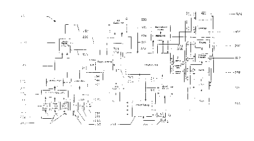
A circuit configuration 250, comprising an exemplary
embodiment of the circuitry of spectrophotometer apparatus 200
which can be utilized in accordance with the invention, is
primarily illustrated in FIG. 4. A number of the components of
the circuit configuration 250 are similar in structure and
function to components of the densitometer apparatus 100
previously described with respect to FIG. 1 in the section
entitled "Background of the Invention." The principal components
of the circuit configuration 250 as shown in FIG. 4 are
relatively well-known in the art and the principal structure of
-21-
the configuration would be apparent to those skilled in the
design of color measurement devices.
As previously described, apparatus 200 comprises a
spectrophotometer apparatus for purposes of providing output data
in the form of spectral characteristics of an object sample 252
under test. As shown in FIG. 4, the spectrophotometer apparatus
200 and the circuit configuration 250 include a light source unit
254 utilized for measuring the spectral response characteristics
of the object sample 252. With reference to FIGS. 2 and 3, for
purposes of measuring the object sample under test 252, the
object sample 252 would be positioned within the shoe window 214
and centrally positioned with respect to the reference patch 213.
In the particular configuration illustrated in FIG. 4, the
spectrophotometer apparatus 200 is adapted to measure spectral
reflection characteristics. However, it should be emphasized
that a calibration arrangement in accordance with the current
invention could also be utilized with apparatus adapted to
measure transmittance or similar characteristics.
Various standards have been developed for spectrophotometer
light source illuminants for spectral reflectance measurements in
various industrial and commercial fields. For example,
standards have previously been described in terms of a tungsten
lamp providing an influx from a lamp operating at a Planckian
distribution of 3000K. Other suggested standards have been
developed by ANSI and the International Organization for
Standardization ("ISO"). In addition, various CIE illuminants
have also been defined, for calculations under various lighting
conditions. Such light source standards are typically defined in
terms of the spectral energy distribution of the illuminant. The
light source 254 preferably conforms to an appropriate standard
and can, for example, comprise a filament meeting a standard
conventionally known in the industry as 2856K ANSI. The light
source or lamp 254 is operated under control of a lamp control
circuit 256, and power to the lamp control circuit 256 can be
-22-
~~~~ =~'~v
provided through a conventional power supply 258 operating under
conventional AC utility power or, alternatively, batteries such
as those shown as batteries 220 in FIG. 3.
Preferably, the light source 254 projects light through a
collimating lens (not shown) which serves to focus the
electromagnetic radiation from the light source 254 into a narrow
collimated beam of light rays. Various types of conventional and
well-known collimating lenses can be employed. Further, the
light rays transmitted through the collimating lens would
typically project through an aperture (not shown), with the
dimensions of the aperture determining the size of the irradiated
area of the object sample 252. Various standards have also been
defined for preferable sizes of the irradiated area. Ideally,
the aperture is of a size such that the irradiance is uniform
over the entire irradiated area. However, in any physically
realizable spectrophotometer arrangement, such uniform irradiance
cannot be achieved. Current standards suggest that the size of
an irradiated area should be such that irradiance measured at any
point within the area is at least 90 percent of the maximum
value. In addition, however, aperture size is typically limited
to the size of the particular areas to be measured, and is also
sized so as to reduce stray light.
The light rays emerging from the aperture (not shown) are
illustrated in FIG. 4 as light rays 260 and are projected onto
the irradiated area surface of the object sample 252 under test.
As the light rays 260 are projected onto the object sample 252
under test, electromagnetic radiation shown as light rays 262
will be reflected from the object sample 252. As previously
described in the section entitled "Background of the Invention,"
it is necessary to obtain quantitative measurements of this
reflected light for purposes of determining the relative
proportions of the light reflected from various segments of the
spectrum and from various object samples. As also previously
described, it is substantially impossible to measure all of the
-23-
.r, '~2 n~ y ~ -;
o~ fJ (~ "~ F,t
light reflected from the object sample 252. Accordingly,
standard detection configurations have been developed, whereby
reflected light is detected at a specific angle relative to the
illumination light rays 260 projected normal to the plane of the
object sample 252. More specifically, standards have been
developed for detection of reflected light rays at an angle of
45° to the normal direction of the light rays 260. This angle of
45° has become a standard for reflectance measurement and is
considered desirable in that this configuration will tend to
maximize the range of the measurements. In addition, however,
the 45° differential also represents somewhat of a relatively
normal viewing configuration of a human observer (i.e.,
illumination at a 45° angle from the viewer's line of sight).
For purposes of providing light detection, bundled fiber
optic circuits or transmission media 264 are provided. As will
be explained in greater detail in subsequent paragraphs herein,
light reflected from the object sample 252 is detected by a
predetermined number of "segmented" detection circuits, with each
circuit corresponding to a different portion of the visible light
spectrum in accordance with the spectral characteristics of the
particular filter associated with that detection circuit. In the
circuit configuration 250 illustrated in FIG. 4, a separate fiber
optic bundle 264 will be provided for each segment, although only
three of the fiber optic bundles 264 are illustrated in FIG. 4.
Each of the fiber optic bundles 264 provides a means for
collecting and receiving the reflected light (shown as light rays
262) from the object sample 252. Although fiber optic bundles
are illustrated in FIG. 4, other types of means for receiving and
collecting the reflected light can be employed without departing
from the principal concepts of the invention.
The light collected from the fiber optic bundles 264 is
applied on symbolic paths 266 to a filtered photocell
configuration 268. For each path or separate segment from a
fiber optic bundle 264, a separate spectral filter is provided.
-24-
~n~r~a~~
As is well-known in the design of spectrophotometers, each of the
filters will have a different spectral frequency response, so
that the entire array of filters will provide an indication of
spectral characteristics of the re:Elected light across the
entirety of the visible light spectrum. For example, each of the
filters (and associated spectral "segments") can have a bandwidth
substantially in the range of 20 nanometers (nms), with each of
the filters having a center frequency spaced apart approximately
20 nms from filters having adjacent frequency responses. That
is, each of the filters will tend to absorb light energy at
frequencies outside of the bandwidth representative of the
particular spectrum portion of the filter. In this manner, with
each of the filters representative of a different "segment" and
different portion of the visible light spectrum, a quantitative
measurement of the light reflected from the object sample and
passing through each filter will provide an indication of the
proportion of light reflected from the object sample within the
particular frequency bandwidth of the filter. Accordingly, for a
given predetermined number of filters or segments, a
corresponding number of "points" can be obtained for the spectral
response characteristic curve for the object sample. As
previously described, a series of sixteen segments and filters,
with each of the filters having a bandwidth of approximately 20'
nms, can be employed. However, various other numbers of filters
and various bandwidth ranges can also be employed without
departing from any of the novel concepts of the invention.
It is apparent from the foregoing that the actual
quantitative measurement of reflectance for a particular segment
is dependent in substantial part on the spectral transmittance
characteristics of the filters. Accordingly, various well-known
standards have been developed with respect to spectral
characteristics of color measurement device filters. For
example, with respect to densitometer apparatus, standards were
previously described for the prior art densitometer apparatus 100
-25-
~~~~~a ~W f~
illustrated in FIG. 1. Again, a variable number of filters and
segments, with corresponding varying bandwidths, can be employed
with the spectrophotometer apparatus 200 in accordance with the
invention.
Continuing to refer to the filtered photocell configuration
268, the configuration 268 can comprise a series of cells such as
photovoltaic sensor cells (not specifically shown outside of the
configuration 268). A sensor cell would be positioned
essentially behind each of the filters, so that the light rays
passing through the filters would impinge on receptor surfaces of
the sensor cells. Accordingly, the configuration 268 would
comprise a separate sensor cell associated with each of the
separate filters. Such sensor cells can comprise conventional
photoelectric elements adapted to detect the light rays emanating
through the corresponding spectral filters. The sensors are
well-known in the art of color measuring device design, and are
preferably adapted to generate electrical currents having
magnitudes proportional to the intensities of the sensed light
rays. Various types of commercially available sensors can be
employed with the photocell configuration 268.
The magnitude of the electrical current comprising an output
signal for each of the filters will be proportional to the
intensity of the reflected light rays transmitted through the
corresponding spectral filter. These light rays will have a
spectral distribution corresponding in part to the product of the
spectral reflectance curve of the object sample 252 under test,
and the spectral response curve of the corresponding filter.
Accordingly, for a particular segment of the visible light
spectrum represented by the spectral response curve of the
filter, the magnitude of the electrical current represents a
quantitative measurement of the proportion of reflectance of the
object sample 252,within the frequency spectrum for which the
filter readily passes visible light.
-26-
c
Continuing to refer to FIG. 4, the electrical currents
representative of the proportion of light passing through the
filters of the photocell configuration 268 are applied on
transmission lines of line group 270. For purposes of
simplification and understanding, the line group 270 is
illustrated in FIG. 4 as comprising a single directional line.
However, in the physically realized circuit configuration 250,
the line group 270 would comprise a separate line pair for each
of the frequency segments and, correspondingly, for each of the
filters and photocells of the configuration 268. That is, a line
pair would be interconnected to each of the photocells of the
configuration 268.
As further shown in FIG. 4, each of the electrical current
signals appearing on pairs of the line group 270 are applied as
input signals to a series of linear amplifier circuits 272.
Again, for purposes of simplification and understanding, the
linear amplifier circuitry 272 is illustrated in FIG. 4 as
comprising a single symbolic element. However, the linear
amplifier circuitry 272 would preferably comprise a separate
linear amplifier for each of the segments of the
spectrophotometer apparatus 200, with each line pair of the line
group 270 interconnected to a separate one of the linear
amplifiers of circuitry 272. The linear amplifiers of the
circuitry 272 can be conventional in structure and function, and
responsive to the electrical current output signals of the
associated photocell sensors to provide a means for converting
low level output current from the respective sensor on the
corresponding input line pair to a voltage level signal generated
as an output signal for each linear amplifier. The voltage level
of the output signal of each linear amplifier is preferably of a
magnitude suitable for subsequent analog-to-digital (A/D)
conversion functions. Such amplifiers are well-known in the
circuit design art and are commercially available with an
appropriate volts per ampere conversion ratio, bandwidth and
-27-
r~",~~~ ~ ~ e~ ~ i ~~ f~J '~
output voltage range. The voltage output signal from each of the
linear amplifiers is applied as an output signal to separate ones
of the line group 274.
The spectrophotometer apparatus 200 also includes a single
side sensor 276 which is utilized to compensate for changes in
lamp intensity of the source light 254 in accordance with the
invention as described in subsequent paragraphs herein. The side
sensor 276 can comprise an appropriate photovoltaic sensor cell
or similar sensor responsive to the light rays 278 emanating from
the source light 254. In known arrangements employing side
sensors for lamp compensation, the spectral response
characteristics of the side sensors are "matched" to the spectral
response characteristics of the particular detection channel or
segment then being compensated. For example, in various
densitometer arrangements, wherein cyan, magenta and yellow color
channels may be employed, it is known to provide for matching the
spectral response characteristic of the side sensor to the
particular channel then being compensated. Such a matching
arrangement may be achieved through the use of multiple side
sensors each having a filter with a spectral response
characteristic matching that of one of the channels of the
densitometer or, alternatively, a single side sensor may be
employed with a series of filters which are individually and
sequentially "moved" into appropriate position so as to provide a
response characteristic matching that of the then currently
evaluated color channel. Similar arrangements have been employed
in other color measuring devices, such as spectrophotometers.
In contrast, and in accordance with the invention, the side
sensor 276 employed in the spectrophotometer apparatus 200 does
not include any "changing" of spectral response characteristics
(e. g. by sequential movement of independent filters into
positions adjacent the side sensor), and further does not include
any components to necessarily match the spectral response
characteristics of the side sensor 276 with spectral response
-28-
characteristics of a segment then being evaluated. If desired,
the side sensor 276 can include an appropriate filter for
filtering out stray light and providing passage of the light rays
278 only within a bandwidth "representative" of the lamp
intensity of the source light 254. Of primary importance is the
concept that the calibration arrangement subsequently described
herein does not require any matching of the side sensor spectral
response with the spectral response characteristics of the
individual segments. As further described in subsequent
paragraphs herein, the calibration procedure utilized in
accordance with the invention includes the determination of a
compensation coefficient (for each segment) which is indicative
of the relationship between changes in tre lamp intensity
detected by the side sensor and changes in the reflectance
intensity detected by filters of the individual segments as the
lamp changes in intensity.
The electrical current output signal from the side sensor
276 generated on line pair 280 is applied as an input signal to
the linear amplifier circuit 282. The linear amplifier circuit
282 can preferably comprise a single linear amplifier having
structure and function similar to the linear amplifiers of the
circuitry 272. That is, the linear amplifier 282 can generate an
appropriate voltage level output signal on line 284 proportiona l
to the electrical current input signal on line 280. As further
shown in FIG. 4, appropriate supply voltage can be applied to the
linear amplifier circuitry 272 and linear amplifier circuit 282
from the supply voltage circuit 286 by means of transmission line
288.
Each of the voltage signal outputs from the linear amplifier
circuitry 272 and 282 are applied as input signals from lines 274
and 284 to multiplexes circuitry 290. Again, it should be noted
that the line group 274 will include separate lines for each
spectrum segment of the spectrophotometer apparatus 200. The
multiplexes circuitry 290 can be conventional in design and
-29-
~" i~ °! ro
~i ~ ~ P9 ~ °.,-~ rvl Jf
comprise a series of one or more conventional multiplexers. The
multiplexes circuitry 290 operates so as to time multiplex the
output signals from the linear amplifier circuitry (including
circuitry 272 and linear amplifier 282) onto the conductive path
292. Timing for operation of the multiplexes circuitry 290 can
be provided by means of clock and similar signals from the
processor 294 via path 296. Operation of the processor 294 will
be described in greater detail in subsequent paragraphs herein.
Again, the structure and function of the multiplexes circuitry
290 is relatively conventional in design. During actual
measurements of the reflectance from the object sample 252, the
spectrophotometer apparatus 200 will utilize the resultant
multiplexed signals on path 292 as sequentially representative
reflectance signals from each of the spectrum segments and each
of the linear amplifiers of the linear amplifier circuitry 272,
and will also represent a voltage output signal corresponding to
the lamp intensity signal from the linear amplifier 282.
The resultant multiplexed signals from the multiplexes
circuitry 290 are applied as output signals on the conductive
path or paths 292. The resultant multiplexed signals are further
applied as input signals to a relatively conventional analog-to-
digital (A/D) converter circuit 298. The A/D converter 298
comprises a means for converting the analog multiplexed signals
on the conductive paths 292 to digital signals for purposes of
subsequent processing by the processor 294. The A/D converter
298 can be conventional in design and may be controlled by timing
and similar pulse signals applied as input signals on conductive
path 300 from the processor 294. Supply voltage for the A/D
converter 298 can be provided by the supply voltage circuit 286
over conductive paths 304. Similarly, the supply voltage circuit
286 can also supply appropriate voltage level signals to the
multiplexes circuitry 290 over the conductive paths 306.
As further illustrated in FIG. 4, the digital output signals
from the A/D converter circuit 298 are applied as input signals
-30-
;;a .~ .l ..~
~.~i~~~l~-~'~'~
on transmission line 302 to the processor 294. The processor 294
is utilized for control of various functions associated with the
spectrophotometer apparatus 200, including calibration methods in
accordance with the invention as described in subsequent
paragraphs herein. Numerous types of conventional and
commercially available processors can be employed for the
processor unit 294. An exemplary processor could, for example,
comprise the Intel 80C31 8-byte CMOS microcomputer commercially
available from the Intel Corporation.
For purposes of general background, FIGS. 5 and 6 illustrate
a general structural diagram of a computer configuration with
generalized components. The arrangement shown in FIGS. 5 and 6
does not necessarily correspond specifically to the processor and
associated component configuration illustrated in FIG. 4.
Instead, FIGS. 5 and 6 are merely for purposes of background
description of a generalized form of a programmable device.
Referring specifically to FIG. 5, a generalized processing unit
400 is illustrated. As shown therein, the processing unit 400
can comprise a relatively conventional microprocessor 402. As
previously described, although various types of well known and
commercially available devices can be employed for the processor
402, a typical internal configuration for processor 402 is
illustrated in FIG. 6, and a brief and simplistic description
thereof will be provided.
Referring specifically to FIG. 6, the processor 402
comprises an internal bus 404 which provides a means for
bidirectional communication between conventional circuit
components of the processor 402. For example, signals can be
transmitted to and received from the program counter 406, which
comprise signals representative of the "next" instruction in the
computer memory to be executed. Communication can also be
provided between the internal bus 404 and processor components
such as the stack pointer 408, general purpose registers 410 and
arithmetic unit 420. Each of these processor components is well
-31-
~~re~~%
known to those skilled in the art of internal computer system
design.
The transmission and reception of data from memories and
other components of the processing unit 400 can be provided by
the data bus 422 which is connected to the internal bus 404
through a conventional data buffer 424 so as to provide
bidirectional communication therewith in the form of multi-digit
parallel binary signals. The internal bus 404 is also connected
to an address bus 426 through an address buffer 428. The
processor 402 can provide, for example, multi-digit parallel
binary address signals on the bus 426 for directed communication
between the processor 402 and the various memories and other
devices having signal communications through the data bus 422.
Conventional system control is provided by interconnection
of the control bus 430 to timing and control circuitry 432.
Communication signals from the conventional timing and control
circuitry 432 can be applied to various components of the
processor 402 through the internal bus 404.
The processor 402 also includes other conventional circuit
components, including an instruction register 434. The
instruction register 434 comprises a register to which the "next"
instruction is stored for purposes of decoding an execution. The
data within the instruction register 434 is applied.to the
instruction decoder 436 which comprises conventional circuitry
for decoding the instruction data received from the next program
location in memory. The processor 402 can also include such
conventional components as a flag register 438 utilized for
various programming control within the processor 402.
The control bus 430 can be characterized as comprising a
series of individual command signal leads. The signal leads can
include "transmitted" commands such as "read," "write," "memory"
and "I/O" commands. In addition, the control bus 430 can be
adapted to apply certain "received" commands to the timing and
control circuitry 432. Such commands can include "wait," "reset"
-32-
r
~~s~~~ ~~
and "interrupt" commands. The use of these commands is well
known in the field of computer system design. For example, if
data is to be read from a certain address location in a memory of
the processing unit 400, "enable" signals can be applied to the
"read" and "memory" command leads from the timing and control
circuitry 432. Correspondingly, the address of the particular
memory location to be read can be transmitted on an address bus
426, while the data to be read from the particular memory
location will be applied to the processor 402 on data bus 422.
Similarly, when data is to be applied to a particular I/O device
associated with the processing unit 400, "enable" signals can be
applied on the "write" and "I/O" signal command leads from the
timing and control circuitry 432. Correspondingly, the address
designation of the I/O device can be applied on address bus 426,
while the particular data to be transmitted to the I/O device can
be applied on data bus 422. Again, the circuitry associated with
processor 402, and processor 402 itself are well known in the
art.
Returning again to FIG. 5, the processing unit 400 includes
memory storage elements such as the random access memory (RAM)
440. The RAM 440 is conventional in design and includes memory
locations wherein data may be stored and modified during
execution of program sequences. Similarly, for stoxage of
"permanent" data or instructions wherein modifications must be
made only occasionally, a conventional erasable-programmable read
only memory (EPROM) 442 is also employed. Both the RAM memory
440 and the EPROM memory 442 are interconnected with the
processor 402 so as to allow control and address location signals
to be applied on the control bus 430 and address bus 426,
respectively. In addition, for purposes of reading data from the
memories into the processor 402, and for writing data into the
memories, bidirectional communication is established between the
RAM memory 440, EPROM memory 442 and the processor 402 through
data bus 422.
-33-
!.t ~~ °~ I
~~ Ei r
For purposes of intercommunication with external devices,
the processing unit 400 can also include a parallel I/O interface
module 444 and a serial I/O interface module 446. The parallel
interface module 444 provides a means for transmitting and
receiving data signals between the processor 402 and external
devices which generate and receive signals in parallel format.
The serial interface module 446 is utilized to interface with
external devices in a serial format.
Like the RAM memory 440 and the EPROM memory 442, the
interface modules 444 and 446 are interconnected to the processor
402 through the control bus 430 and address bus 426 for purposes
of applying control and address information data signals,
respectively, to each of the modules. In addition, the interface
modules 444 and 446 are interconnected to the processor 402
through data bus 422 so that data signals are bidirectionally
transferrable between the modules 444, 446 and processor 402. It
should be emphasized that the general circuitry of the processing
. unit 400 and the functional operations associated therewith are
well known in the field of computer system design.
The aforedescribed processor configuration as illustrated in
FIGS. 5 and 6 is merely exemplary of certain of the general
concepts associated with processor and associated component
design. In the particular embodiment illustrated in FIG. 4, the
processor is illustrated as a separate processing unit 294
independent of the memory and similar elements. As further shown
in FIG. 4, the processor 294 can provide control signals to both
the supply voltage circuitry 286 and lamp control circuitry 256
via transmission paths 308 and 310, respectively. Control
signals can also be applied from the processor 294 to the power
supply circuit 258 via path 312. In addition, such control
signals can be applied to reset circuitry 314 which, in turn, can
also apply, as input signals to the processor 294, reset signals
via path 316. Although FIG. 4 further illustrates other
interconnections among components such as the power supply
-34-
sf i
~~~~,~J:~v
circuitry 258 and reset circuitry 314, the structure and function
of such interconnections will be apparent from the illustration
of FIG. 4 and other detailed descriptions set forth herein.
The spectrophotometer apparatus 200 can also comprise a
conventional address decoder 320 interconnected to the address
bus of the bus configuration 322 for the processor 294. The
address decoder 320 is utilized to decode the address range for
the various devices associated with the bus configuration 322.
Such an address decoder configuration is convention in design.
The apparatus 200 can also include a conventional EPROM 324
which can comprise, for example, a CMOS 512K EPROM. In addition,
the spectrophotometer apparatus 200 can also comprise a random
access memory (RAM) 326. The RAM 326 can, for example, comprise
an 8192 byte static random access memory.
As previously described, the spectrophotometer apparatus 200
can also include a series of keys 243. These keys 243 provide a
means for manual input of data by the spectrophotometer operator.
Still further, the apparatus 200 further includes the display 240
for purposes of providing data display to the operator. In
association with the aforedescribed components which are directly
or indirectly connected to the bus configuration 322 of the
processor 294, conventional latching circuitry 326 is also
employed for purposes of latching data applied to and from the .
bus configuration 322.
As further shown in FIG. 4, the processor 294 is
interconnected to a conventional RS232 I/O interface circuit 328.
The interface circuit 328 provides an interface to an external
computer or printer device 330, for purposes of transmitting and
receiving data to and from the interface device, respectively.
Control signals from the processor 294 to the interface 328 can
be applied via path 332. Correspondingly, data from the
processor 294 can be applied as input data through the interface
328 via transmission path 334. Correspondingly, data from the
computer printer device 330 can be applied through the interface
-35-
G? ; ,~ r c
~a~t~e2~~J~~
328 and input to the processor 294 by means of transmission path
336.
The foregoing provides a brief description of various of the
components of the circuit configuration 250 of the
spectrophotometer apparatus 200. Many of these components are
also utilized in various other types of color measurement
apparatus. For example, a detailed description of similar
components for use in a densitometer are described in detail in
the commonly assigned Cargill et al U.S. Patent Application
Serial No. 309,342, filed February 10, 1989. Concepts associated
with the use of a color measurement device and an interface for
communication with external devices are disclosed in the commonly
assigned Peterson et al U.S. Patent No. 4,591,978, issued May 27,
1986.
In brief summary, the apparatus 200 is adapted to operate as
an automated instrument for providing a spectral reflectance
analysis of object samples. When the object sample is positioned
appropriately in the spectrophotometer apparatus 200, light from
the source 254 is projected onto the surface 252 of the sample,
and reflected light rays 262 are received by the fiber optic
bundles 264. A separate fiber optic bundle 264 is provided for
each spectral segment to be analyzed by the apparatus 200. The
light rays passing through the fiber optic bundles 264 are
applied to a configuration of filters and photocells 268. Each
of the filters will substantially pass the reflected light only
within the bandwidth corresponding to the particular segment.
Electrical current signals generated from the photocells of the
configuration 268 are applied to linear amplifier circuitry 272,
and voltage output signals are generated therefrom.
Correspondingly, the intensity of the light rays 278 from the
light source 254 is detected by the side sensor circuit 276.
Electrical current signals representative of this intensity are
applied as input signals to the linear amplifier 282, and a
corresponding voltage level output signal is generated therefrom.
-36-
~~»~~~~~
The voltage signals from the linear amplifier circuitry 272
and 282 are applied as input signals to the multiplexes circuits
290. The multiplexes circuits 290 provide time multiplexed
signals which are applied as input signals to the A/D converter
298. The converter 298 converts the analog signals to
appropriate digital signals, and applies the same to the
processor 294. The processor 294 can be utilized to perform
appropriate computations and measurements of the digital signals
from path 302 so as to generate data indicative of the spectral
reflectance characteristics of the object sample 252 for each of
the spectral segments. As desired, this data can be visually
displayed to an operator through the display 240.
Correspondingly, such data can be applied to the external devices
330 through the interface 328. Control of the processor 294 can
be provided, at least in part, through operator input from the
keys 243. The general operation of spectrophotometers, given
spectral data from a series of segments, is relatively well known
in the art.
In accordance with the invention, and as previously
described in part, it is desirable to "calibrate" the
spectrophotometer apparatus 200. In part, this calibration is
provided for purposes of compensating for changes in lamp
temperature and intensity. A calibration or lamp compensation
arrangement in accordance with the invention will now be
described in the following paragraphs. This compensation
arrangement is also illustrated as a series of sequence diagrams
in FIGS. 7, 8 and 9. The actual functions performed with respect
to various computations and similar procedures are preferably
performed by computer software operating with the processor 294.
For purposes of calibration and lamp compensation, a
reference sample is utilized by the operator, in place of an
actual object sample to be tested. However, the principal
operations of the spectrophotometer apparatus circuit
configuration 250 illustrated in FIG. 4 are essentially
-37-
4', s'? r< ~~ et r~ y
substantially the same, with a reference sample replacing the
conventional object sample under test. That is, the operation of
the various optics circuitry for obtaining spectral reflectance
characteristics is performed as previously described.
For purposes of calibration and lamp compensation, a
reference sample can be provided by the apparatus manufacturer,
along with the specific apparatus itself. The reference sample
can include, for example, a "white spot" reference. With the
white spot reference, reflectance data comprising actual data for
the white spot measured at the manufacturer's facilities can also
be provided to the operator. Such data will be referred to in
subsequent paragraphs herein as the "desired" reflectance data.
Such data would be in the form of, for example, reflectance
percentages for each of the spectral segments. This data
provides a basis for relating voltage signal levels to
reflectance percentages for the particular instrument. That is,
without such data representing previously measured reflectances,
the initial relationship of signal levels to reflectances for
this particular instrument would be unknown. In addition to
providing printed information describing the desired reflectance
data for the operator, such data can also be prestored by the
apparatus manufacturer within appropriate memories of the
processor 294.
For purposes of performing the calibration and lamp
compensation methods in accordance with the invention, the
reference sample comprising the "white spot" reference can be
placed in the spectrophotometer apparatus 200 as previously
described with respect to FIGS. 2 and 3. Thereafter, the
operator can "select" the calibration procedures to be performed
by appropriate input of data via the keys 243. When the operator
enters the appropriate data through the keys 243, the processor
294 and associated components will recognize that the calibration
procedure is to be performed, and various initialization
procedures (clearing of memories, etc.) can be executed.
-38-
~ C
Following such initialization, various automatic calibration
procedures can be performed with respect to errors which may be
caused by allowed tolerances of the various electronics of the
circuit configuration 250. Such calibration procedures are
relatively well known in the color measurement arts, and do not
form any of the principal concepts of the present invention.
That is, such calibration procedures are substantially separate
and distinct from the calibration and lamp compensation
procedures in accordance with the present invention.
For purposes of performing the lamp compensation procedures,
the circuit configuration 250 will utilize the desired
reflectance data for the reference sample. As previously
described, such desired reflectance data can be entered by the
operator at the time of performance of the lamp compensation
procedures or, alternatively, can comprise prestored data then
currently stored in appropriate memories of the circuit
configuration 250. Accordingly, the processor 294 can contain
appropriate software to "prompt" the operator (through signals
provided via the display 240) as to whether such prestored
desired reflectance data should be utilized or, alternatively,
whether the operator wishes to enter desired reflectance data.
As shown in FIG. 7, if the operator wishes to enter the
desired reflectance data, the apparatus 250 can be adapted to, .
prompt the operator (again through signals applied to the display
240) for the operator to enter the desired reflection data
through the keys 243.
For purposes of subsequent description herein, the letter
notation "x" will represent a selected spectral segment for the
various measurements to be performed by the apparatus 200.
Correspondingly, the letter notation "a" will represent a present
or current measurement of a sequence of measurements to be
performed as described herein.
With these notations, for purposes of describing the desired
reflectance data, the notation WRx will represent the value of
-39-
~l~r~~~~
the desired reflectance data for spectral segment x, whether such
data is in the form of prestored data or data then entered by the
operator. As the operator enters t:he desired reflectance data,
such data is stored and a determination is made as to whether
data for all spectral segments has been received. If not, the
apparatus 200 can continue to prompt the operator for additional
reflectance data until data representative of all segments is
stored in the appropriate memories of processor 294.
Correspondingly, it is apparent that the processor 294 can be
programmed so that the operator can enter desired reflectance
data only for a subset of the entirety of the segments, with the
desired reflectance data for the other segments corresponding to
prestored data.
After the desired reflectance data for all segments has been
stored within appropriate memories of the processor 294, a
determination can be made as to the elapsed time since a prior
measurement has been performed by the apparatus 200. A primary
purpose for this determination is that a first measurement to be
performed by the apparatus 200 is to be essentially characterized
as a "cold lamp" measurement. Accordingly, if insufficient time
has elapsed since the lamp of the light source 254 has previously
been activated, the first measurement to be taken during the lamp
compensation procedure may occur prior to the time that the lamp
"cooled" sufficiently since a previous measurement. If
insufficient time has elapsed since a last measurement utilizing
the lamp of the source 254, the apparatus 200 can provide an
automated delay before a first measurement is performed. The
actual elapsed time for such delay should be sufficient so as to
assure that a first reading is performed with a "cold lamp", and
a warm up characteristic can be obtained through the lamp
compensation measurements.
When sufficient time has elapsed since the last measurement,
a first reading of the reflectance sensor values for each of the
segments can be obtained, in accordance with the reflectance
-40-
~~3~~
measurement procedures previously described with respect to the
circuit configuration 250 illustrated in FIG. 4.
Correspondingly, a first reading is also obtained of the
intensity measurement of the lamp of light source 254 through the
side sensor 276. Data representative of the reflectance sensor
measurement values for each segment, and data representative of
the side sensor measurement value can then be stored in
appropriate memories of the processor 294.
Following the first reading, and in accordance with the
invention, a plurality of additional readings of the reflectance
sensor measurement values and side sensor measurement values can
be performed, as the lamp of the light source 254 begins to "heat
up." In this regard, and in accordance with the invention, the
calibration and lamp compensation procedure comprises, in part, a
timed sequence of reflectance sensor measurements and side sensor
measurements. Therefore, and as shown in FIG. 8, following such
measurements, a determination can be made as to whether the
appropriate number of measurements have been completed. If not,
an appropriate measurement sequence number can be updated. In
addition, and in accordance to the invention, the measurements
are obtained at predetermined time intervals. Accordingly, the
circuit configuration 250 can be adapted to determine if the
appropriate sequence interval time has elapsed. If not, a delay
will occur and a determination of whether the sequence interval
time has elapsed can be periodically executed. When the
appropriate sequence interval time has elapsed, and assuming that
all measurements have not been completed, a new set of
reflectance sensor measurement values and side sensor measurement
value can be obtained and stored in appropriate memory. For
purposes of description, the side sensor measurement values are
referred to in subsequent paragraphs herein as values SS1, SS2, .
. . SSN, where N represents the total number of measurements to
be performed within the lamp compensation sequence.
Correspondingly, the reflectance sensor measurement values for a
-41-
particular segment x are referred to herein as reflectance sensor
measurement values RSlx, RS2x, . . . RSNx, where N again
represents the total number of measurements within the
measurement sequence.
The lamp compensation procedure in accordance with the
invention is not limited to a particular number of measurements N
or a particular timed sequence interval between measurements.
However, the number of measurements and the sequence interval
should be sufficient so that a "warm-up" characteristic is
obtained with respect to the light source 254. For example,
experimentation has shown that a series of five measurements may
be utilized, with the measurements spaced at intervals of
approximately three seconds.
Following the measurements of the side sensor values and the
reflectance sensor values, the circuit configuration 250 can be
adapted to determine a filter compensation coefficient for each
segment. With the filter compensation coefficient for a segment
x referred to as coefficient CCx, the coefficient can be
determined in accordance with the following:
CCx = ((RSlx/RSNx) - 1)/((SS1/SSN) - 1) (Equation 2)
where RSlx represents the reflectance sensor measurement value
for the first measurement for segment x, RSNx represents the
reflectance sensor measurement value for the last measurement for
segment x, SS1 represents the side sensor measurement value for
the first measurement, and SSN represents the side sensor
measurement value for the last measurement. Again, the filter
compensation coefficient is a compensation value which is
provided separate and independent for each spectral segment.
-42-
~~ v ri c)
To further explain the concept of the compensation
coefficients, reference is made to earlier description relating
to the structural configuration of the side sensor 276
illustrated in FIG. 4. As previously described, one of the
concepts of the invention is the lack of any necessity of
matching the spectral response characteristics of the side sensor
to the spectral response characteristics of individual segments.
Prior art system employing side sensors would typically utilize
multiple side sensors with filters having differing response
characteristics matching response characteristics of the
detection channels or segments, or would otherwise utilize a
single side sensor with multiple filters which could be "moved"
into position adjacent the side sensor for providing differing
response characteristics matching the channels or segments. As
earlier described, and in accordance with the invention, the side
sensor 276 can employ a fixed spectral response, with the
spectral response not necessarily being of the same .
characteristic as any given segment. With a change in intensity
of the lamp of the light source 254, a corresponding change will
be detected by the side sensor. Further, however, a
corresponding change in reflection intensity will also occur with
xespect to each of the segments. It is the determination of the
compensation coefficient which provides an indication of the
relationship between the change in the side sensor detected
intensity and the change in reflection intensity detected by a
segment as the lamp correspondingly changes in intensity. That
-43-
is, the compensation coefficient for a given segment represents a
ratio of change in the reflectance sensor measurement to a change
in the side sensor measurement. By utilizing the compensation
coefficients for calibration as described in subsequent
paragraphs herein, spectrophotometers in accordance with the
invention avoid the expense and circuit complexity of requiring
multiple sensors with differing spectral response characteristics
or individual side sensors requiring movable filters or the like
to adjust the side sensor response characteristics.
Following the determination of the filter compensation
coefficients, the previously stored reflectance sensor
measurement values can be normalized. With a normalized
reflectance sensor measurement value referred to as RScxa, where
x represents the particular spectral segment and a represents the
current measurement, these normalized reflectance measurement
values can be determined in accordance with the following:
RScxa = RSxa [(((SS1/SSa) - 1) CCx) + 1] (Equation 3)
where RSxa represents the reflectance sensor measurement value
for segment x and measurement a, SS1 represents the side sensor
measurement value for the first reading, SSa represents the side
sensor measurement value for the current measurement, and CCx
represents the filter compensation coefficient for the current
spectral segment. The normalized reflectance measurements
-44-
essentially represent compensation ~of the reflectance sensor
measurements for changes in side sensor measurements which are
adjusted by known differences in their drifts.
Using the normalized reflectance sensor measurement values,
a scale value can then be determined for each segment. This
scale value, referred to herein as WSx for segment x, essentially
represents the conversion of a measured reflectance quantity to a
percentage reflectance for the segment. That is, the scale
factor conversion provides a value representative of the portion
(as a percentage) of source light which is reflected from the
sample, for the portion of the spectrum represented by the
segment and corresponding filter. This value can be
characterized as the filter reflectance or the reflectance for
the particular segment. A scale value for each of the spectral
segments can be determined in accordance with the following:
WSx = [(RSclx + RSc2x + ...RScNx)/N]/WRx (Equation 4)
where RSclx represents the normalized reflectance sensor
measurement value for the first measurement reading and for the
current segment x, RSc2x represents the normalized reflectance
sensor measurement value for the second measurement reading and
for segment x, and RScNx represents the normalized reflectance
sensor measurement value for measurement reading N and segment x.
-45-
V ,~
Also, WRx represents the desired re:Electance value previously
stored for segment x.
In accordance with the foregoing, a compensation arrangement
is provided whereby a series of readings are obtained, including
a "cold" lamp reading. Reflectance readings thereafter within
the timed sequence are essentially normalized back to the first
reading. With the determination of the filter compensation
coefficient, the normalized reflectance sensor measurement values
and the scale value, appropriate and.sufficient data is obtained
for purposes of subsequent compensation of actual reflectance
sensor measurement values obtained from object samples under
test. More specifically, the compensated reflectance measurement
value for an object sample under test, and for segment x, can be
referred to as Rx. This compensated reflectance value can be
determined in accordance with the following:
Rx = WSx [RSx ((CCx ((SS1/SS) - 1)) + 1)] (Equation 5)
where WSx represents the scale factor for segment x, RSx
represents the actual measured reflectance sensor value for
segment x_, CCx represents the filter compensation coefficient for
segment x, SS1 represents the side sensor measurement value for
the first reading obtained during the lamp compensation
procedure, and SS represents the side sensor measurement value
obtained during the current measurement. In this manner, a
-46-
~~~'~~~4
compensation arrangement is obtained for compensating for various
lamp characteristics.
In accordance with another aspect of a lamp compensation
arrangement in accordance with the invention, it is also possible
to include compensation for temperature. That is, a long-term
temperature coefficient can be applied to each of the spectral
segments and to the side sensor.
For purposes of describing the temperature compensation
arrangement in accordance with the invention, reference is again
made to Equation 5, where an actual reflectance sensor
measurement for segment x is shown as RSx. To provide for
temperature compensation in accordance with the invention, the
quantity RSx can be replaced within Equation 5 by the following:
RSx --> RSx (1 + (Kx * Tc)) (Equation 6)
. where Kx represents a temperature coefficient determined for
segment x, and Tc represents the difference between a temperature
measured during the first lamp compensation calibration reading
and a present temperature reading. The temperature coefficient
Kx essentially represents the concept that for a given change in
temperature, the reflectance sensor will correspondingly change
by a certain percentage. To provide for the temperature
compensation as shown in Equation 6, the circuit configuration
250 illustrated in FIG. 4 can include conventional means for
-47-
determining temperatures occurring at various reference sample
readings and object sample readings.
To provide for further temperature compensation, a
compensation arrangement can also be provided for the side sensor
measurement. Referring again to Equation 5, the side sensor
measurement value obtained during the then-current measurement is
shown as reading SS. For purposes of providing for temperature
compensation, the term SS within Equation 5 can be replaced in
accordance with the following:
SS --> SS (1 + (Ks * Tc)) (Equation 7)
where Ks represents a temperature coefficient obtained for the
side sensor, and Tc again represents the difference between the
temperature measured during the first calibration reading, and
the present reading. Such temperature coefficients can be
obtained through use of external test equipment.
In accordance with the foregoing, the spectrophotometer
apparatus 200 can be utilized for performance of determining
spectral response characteristics of object samples under test.
In addition, and in accordance with the invention, the
spectrophotometer apparatus 200 can include apparatus and methods
for performance of various calibration and lamp compensation
procedures. However, it should be emphasized that the principles
of the calibration and lamp compensation procedures are not
-48-
limited to the specific spectrophotometer apparatus 200 described
herein. In fact,,~the procedures can be employed with apparatus
other than spectrophotometers. Still further, the features of
the calibration and lamp compensation procedures described herein
and in accordance with the invention are not in any manner
necessarily limited to a specific number of spectral segments or
the like. A different number of segments and filters having
various bandwidths can be employed without departing from the
novel concepts of the invention. It will be further apparent to
those skilled in the art that additional modifications and
variations of the above-described illustrative embodiment of the
invention may be effected without departing from the spirit and
scope of the novel concepts of the invention.
-49-