Note: Descriptions are shown in the official language in which they were submitted.
203753~
DEMODULATING SYSTEM CAPABLE OF
ACCURATELY EQUALIZING RECEIVED SIGNALS
USING ERROR CORRECTION CODES
Background of the Invention:
This invention relates to a demodulating system
for demodulating a modulated signal produced by
modulating a carrier signal by error correcting coded
5 transmission data.
A conventional demodulating system comprises an
adaptive equalizer for adaptively equalizing the
modulated signal into an equalized signal in accordance
with polarity signals and discrimination error signals.
10 A demodulator demodulates the equalized signal into
demodulated signals and the discrimination error
signals. The demodulated signals comprise polarity bits
and other data bits. Supplying lines supply the
polarity bits to the adaptive equalizer as the polarity
15 signals. An error-correcting decoder is supplied with
the demodulated signal and produces error location
signals representative of location of error in the
2 203753S
demodulated signals, and corrects error in the
demodulated signals by using the error location signals
into decoded signals.
As will later be described more in detail, the
5 conventional demodulating system is defective in that
the adaptive equalizer can not remove distortion which
appears in a propagation path because the discrimination
error signals have a wrong value under the influence of
big thermal noise which is inevitably superposed on the
10 demodulated signal while propagated through the
propagation path to the demodulating system.
Summary of the Invention:
It is therefore an object of the present
invention to provide a demodulating system capable of
15 correcting discrimination error signals and can remove
distortion which appears in a propagation path.
On describing the gist of an aspect of this
invention, it is possible to understand that a
demodulating system is for demodulating a modulated
20 signal produced by modulating a carrier signal by error
correction coded transmission data and includes: (a)
adaptive equalizing means for adaptively equalizing the
modulated signal into an equalized signal in accordance
with polarity signals and corrected discrimination error
25 signals; (b) demodulating means for demodulating the
equalized signal into demodulated signals and
discrimination error signals, the demodulated signals
being reproduced data bits of said correction coded
203~53S
transmlsslon data and comprlslng polarlty blts and other data
blts; (c) polarlty slgnal supplylng means for supplylng the
polarlty blts to the adaptive equallzlng means as the polarlty
slgnals; (d) error-correctlon code decodlng means for
produclng error locatlon slgnals representative of locatlon of
errors ln sald demodulated slgnals and for error correctlng
and decodlng the demodulated slgnals by uslng the error
locatlon slgnals; and (e) error slgnal correctlng means
connected to the demodulatlng means, the error-correctlon code
decodlng means, and sald adaptlve equallzlng means, for
correctlng the dlscrlmlnatlon error slgnals lnto said
corrected dlscrlmlnatlon error slgnals ln accordance wlth the
error locatlon slgnals and supplylng the corrected
dlscrlmlnatlon error slgnals to the adaptlve equallzlng means.
On descrlblng a dlfferent aspect of thls lnventlon,
lt ls posslble to understand that a demodulatlng system ls for
demodulatlng a modulated signal produced by modulatlng a
carrler slgnal by error correctlon coded transmlsslon data and
lncludes: (a) demodulatlng means for demodulatlng the
modulated slgnal lnto demodulated slgnals comprlslng data blts
representatlve of the error correctlon coded transmlsslon data
contalnlng polarlty blts representatlve of polarltles of the
demodulated slgnals; (b) adaptlve equallzlng means for
adaptively equallzlng the demodulated slgnals ln accordance
wlth polarlty slgnals and corrected dlscrlmlnatlon error
slgnals to output equallzed slgnals and dlscrlmlnatlon error
slgnals; (c) polarlty slgnal supplylng means for supplylng the
polarlty blts to the adaptlve equallzlng means as the polarlty
-- 3
64768-237
2037535
slgnals; (d) error correctlon code decodlng means for
produclng error locatlon slgnals representatlve of locatlon of
errors ln sald equallzed slgnals and for error correctlng and
decodlng the equallzed slgnals by uslng the error locatlon
slgnals lnto decoded slgnals; and (e) error slgnal correctlng
means connected to the adaptlve equallzlng means and the
error-correctlon code decodlng means for correctlng the
dlscrlmlnatlon error slgnals lnto corrected dlscrlmlnatlon
error slgnals ln accordance wlth the error locatlon slgnals
and supplylng the corrected dlscrlmlnatlon error slgnals to
the adaptlve equallzlng means.
Brlef Descript lon of the Drawlnqs:
Flg. 1 ls a block dlagram of a conventlonal
demodulatlng system;
Flg. 2 ls a block dlagram of an adaptlve equallzer
used ln the demodulatlng system deplcted ln Flg. l;
Flg. 3 ls a dlagram for use ln descrlblng operatlon
of the demodulatlng system lllustrated ln Flg. l;
Flg. 4, on the flrst sheet of drawlngs, ls a block
dlagram of a dlfferent conventlonal demodulatlng system;
Flg. 5 ls a block dlagram of a demodulatlng system
accordlng to a flrst embodlment of thls lnventlon;
Flg. 6 ls a block dlagram of an error correctlng
decoder and an error slgnal correctlng clrcult used ln the
demodulatlng system deplcted ln Flg. 5; and
Flg. 7, on the fourth sheet of drawlngs, ls a block
dlagram of a demodulatlng system accordlng to a second
embodlment of thls lnventlon.
-- 4
64768-237
,.. ~
203753~
Descrlptlon of the Preferred 13mbodlment
Referring to Flgs. 1, 2, and 3, a conventlonal
demodulatlng system wlll be descrlbed at flrst ln order to
facllltate an understandlng of the present lnventlon.
The demodulatlng system ls for demodulatlng a
modulated slgnal produced by QAM (Quadrature Amplltude
Modulatlon) modulatlng a carrler slgnal by a sequence of error
correctlng coded transmlsslon data. For example, the error
correctlng codes are glven by Bose-Chaudhurl-Hocquenghem (BCH)
codes or Lee codes.
In Flg. 1, the demodulatlng system comprlses an
adaptlve equallzer 11 whlch ls supplled wlth the modulated
slgnal and ls for adaptlvely equallzlng the modulated slgnal
lnto an equallzed slgnal ln accordance wlth polarlty slgnals
Dp and Dq and dlscrlmlnatlon error slgnals Ep and Eq. A
demodulator 12 demodulates the equallzed slgnal lnto
demodulated slgnal Sll, S12, S21, and S22 and the
dlscrlmlnatlon error slgnals Ep and Eq supplled back to the
adaptlve equallzer 11.
The demodulated slgnals Sll, S12, S21, and S22 are
supplled to an error-correctlng decoder 13. Supplylng llnes
14 supply the polarlty blts Sll and S12 to the adaptlve
equallzer 11 as the polarlty slgnals Dp and Dq.
The error-correctlng decoder 13 produces error
locatlon slgnals representatlve of locatlon of errors ln the
demodulated slgnals. The error-correctlng decoder 13 correct
errors ln the demodulated slgnals by uslng the error locatlon
slgnals lnto decoded slgnals Sll', S12', S21', and S22'.
-- 5
64768-237
203753~
Turnlng to Flg. 2, the adaptlve equallzer 11 ls a
three tapped equallzer wlth an IF band transversal fllter
supplled wlth slxteen QAM waves as lts lnput modulated carrler
slgnal. The descrlptlon hereunder generally applies to any
value of L (L 5 m , m belng an lnteger not smaller than 2) and
to an N-tapped (N belng a posltlve lnteger and lndependent of
L and m) equallzer wlth an IF band transversal fllter.
A radlo slgnal ls plcked by an antenna (not shown)
and fed to a recelvlng sectlon 20. Produced from the
recelvlng sectlon 20, an IF slgnal S0 ls delayed by a flrst
delay clrcult 210 to provlde a flrst delayed slgnal Sl and
subsequently further delayed by a second delay clrcult 211
lnto a second delayed slgnal S2. The IF slgnal S0 ls branched
and then multlplled ln varlable tap galn clrcults 221 and 231
by control slgnal ~ 1 and d l supplled from lntegrator
clrcults 281 and 291 havlng a resettlng functlon.
The second delayed slgnal S2 ls branched and
multlplled ln varlable tap galn clrcults 222 and 232 by
control slgnals ~ and dl dellvered from lntegrator clrcults
282 and 292 havlng a resettlng functlon. The flrst delayed
slgnal Sl and output slgnals of the varlable tap galn clrcults
221 and 222 are summed by a slgnal summlng clrcult 233 lnto a
sum slgnal RS. On the other hand, output slgnals of the
varlable tap galn clrcults 231 and 232 are syntheslzed by a
slgnal summlng clrcult 234 lnto a syntheslzed slgnal IS. The
slgnals RS and IS are comblned by a 90-dlrectlonal coupler
240 lnto a composlte slgnal so that thelr phases are ln a
quadrature relatlon to each other. The composlte slgnal ls
-- 6
64768-237
.
203753~
then provided to a coherent detector clrcult 241 supplled wlth
a recovered carrler from a carrler recovery clrcult 244. The
coherent detector clrcult 241 detects the lnput modulated
carrler slgnal thereby to generate two tralns of baseband
slgnals Dp' and DQ'. Many methods for carrler recovery are
known ln the art, such as the baseband processlng technlque
dlsclosed ln Unlted States Patent No. 3,983,499.
An asynchronlsm detector clrcult 245 ls for
detectlng asynchronlsm ln a carrler recovery loop. Such
clrcults are dlsclosed ln, among others, Japanese Patent
Publlcatlon No. 55-34619 and Unlted States Patent No.
4,121,166. Another method of asynchronlsm detectlon ls
monltorlng the blt error rate and, when lt surpasses a
prescrlbed level, lmposlng lnltlal level resettlng, ln the
manner revealed ln Unlted States Patent No. 3,721,959.
64768-237
20375~5
A decision/error signal generator circuit
(analog to digital converter) 242 monitors the two
trains of polarity signals Dp and DQ and, by detecting
the deviation between the baseband signals Dp' and DQ'
5 and any one of four preset levels, supplies
discrimination error signals Ep and EQ in order to
control the tap gain circuits 221, 222, 231, and 232.
The ZF (zero forcing) algorithm corrects each tap
coefficients Cjk of the tap gain circuits 221, 222, 231,
10 and 232 by the use of these discrimination error signals
Ep and EQ in accordance with the steepest possible
descent method to minimize the cusp or peak levels of
waveform distortions. The ZF algorithm is carried out,
for example, by using the following equations, in which
15 all variables are given in (two-dimensional) complex
numbers except for a.
K
C 1) = Cjk ~ a Sgnk~lD (k-j) k (1)
Cjk = rjk + idjk' (2)
Ek = EPk + iEQk '
20 and (k-j) Dp(k_;) ~ iDQ(k j)~ (4)
where:
j is the tap number,
k is the time,
~ is a fixed incremental step size of the tap
5 setting,
D*(k j) is the complex conjugate of D(k j)~ and
sgn represents the polarity.
2037535
When the real and lmaglnary number parts are
rearranged supposlng that K ls equal to 1 ln the manner usual
ln actual clrcults, the followlng equatlons hold:
~tk+~ k ~ ~ ~sgn(EpkDp~k-~) + EQkDQ(k-~)) (5)
d~(k+l) =d~k ~~ sgn(EQkDp(k ~) ~ EPkDQ(k ~ (6)
where the ZF algorlthm ls used, all the varlables ln these
equatlons are blnary numbers and can be readlly sub~ected to
loglcal operatlon by a dlgltal clrcult. Products and sums are
calculated by excluslve OR clrcults (EORs) 251-253 and 257-
259, excluslve NOR clrcults (ENORs) 254 and 260, reslstors
261-264 and 267-270, and 267-270. The successlve correctlon
of taps ln Equatlons (5) and (6) can be readlly reallzed by
the use of the lntegrators 281, 282, 291, and 292 havlng a
resettlng functlon as tlme-averaglng clrcults. Supposlng
here, wlth a vlew to explalnlng the control slgnals of Flg. 1,
that ~ = l (tap l) and that the tlme k ls a flxed tlme,
namely, k = 0, thereby omlttlng k, the second term of the
rlght slde of equatlons (5) and (6) are transformed lnto:
~Ep .Dp(_l) + EQ~ DQ(_l)~ ~
and A-~EQ~Dp(-l) + Ep~ DQ(_l)~ (8)
The symbol sgn ln Equatlons (5) and (6) becomes unnecessary
under the condltlon that the blnary varlables are loglc
operated. Here Dp( l) and DQ( l) can be readlly derlved ln
correspondence to slgnals whlch are "one blt" behlnd Dp and
DQ. By the use of shlft registers 273 and 274, the EORs 257-
259, and the
~ '
~ 64768-237
20375~S
ENOR 260, multiplication can be carried out as above.
In the case of j = 1, and where Dp and DQ can not be
advanced by one bit, Ep and EQ are delayed by one bit so
that Dp and DQ are in effect advanced one bit with
5 respect to the discrimination error signals Ep and EQ.
The above-described multiplication can be likewise
achieved by shift registers 271 and 272, the EORs
251-253, and the ENOR 254. The equalizer correlates the
discrimination error signals Ep and EQ and the
10 demodulated polarity signals Dp and DQ by a relationship
wi.th respect to time, determines a time position of the
occurrence of an intersymbol interference (waveform
distortion), and eliminates this waveform distortion by
controlling the variable tap gain circuits 221, 222,
15 231, and 232 at the corresponding tap. Inasmuch as
waveform distortions include inphase and quadrature
distortions, the variable tap gain circuits 221-222 and
231-2~2 are needed to obtain the sum signal RS and the
synthesized signal IS which are combined by the use of
20 the 90 coupler 240.
A clock pulse signal is supplied from a clock
synchronizer circuit 243 to the decision/error signal
generator circuit 242 and the shift registers 271-274 to
generally synchronize the system.
Turning back to Fig. 1, the error correcting
decoder 13 is supplied with the demodulated signals Sll,
S12, S21, and S22 produced by the decision circuit 242
described in conjunction with Fig. 2. The error
11 2037535
correcting decoder is a BCH decoder which comprises
error location detection circuits for producing the
error location signals representative of location of
error in each of the demodulated signals Sll, S12, S21,
5 and S22. The BCH decoder comprises an error correcting
circuit for correcting errors in the demodulated signals
Sll, S12, S21, and S22 to produce corrected signals by
using the error location signals and decodes the
corrected signals into the decoded signals Sll', S12',
10 S21', and S22'.
Referring to Fig. 3, the four signal levels of
the demodulated signals are indicated at A, B, C, and D.
The four signal levels have two subsignal levels.
A signal b (shown by black circle) must be in
15 level B. Supposing that the signal b is influenced by
thermal noise, the signal b moves upwardly of Fig. 3 to
become another signal b' indicated by a white circle.
In this case, the error signal Ep must be kept at "1".
The signal b' is located in level A. As a result, the
2n error signal Ep has an erroneous value of "O".
Even in this event, the error correcting decoder
13 can correct errors of the demodulated signals Sll and
S21. No circuitry is, however, used in correcting the
error signal Ep, which is therefore supplied to the
25 adaptive equalizer 11 without correction. As the
adaptive equalizer 11 equalizes the modulated signal in
accordance with erroneous discrimination error signals,
203753~
the adaptlve equallzer 11 can not equallze the modulated
slgnal properly.
In Flg. 4, a dlfferent conventlonal demodulatlng
system comprlses a demodulator 41 whlch ls supplled wlth a
modulated slgnal and ls for demodulatlng the modulated slgnal
lnto demodulated slgnals. An adaptlve equallzer 42 adaptlvely
equallzes the demodulated slgnals ln accordance wlth polarlty
slgnals Dp and Dq and error slgnals Ep and Eq, and outputs
equalized slgnals Sll, S12, S21, and S22 and error slgnals Ep
and Eq. Supplylng llnes supply the polarlty blts to the
adaptlve equallzer 42 as the polarlty slgnals Dp and Dq. An
error-correctlng decoder 43 produces error locatlon slgnals
representatlve of locatlon of errors in the equallzed slgnals
Sll, S12, S21, and S22, and corrects the errors ln the
equallzed slgnals lnto decoded slgnals Sll', S12', S21', and
S22 .
In the dlfferent conventlonal demodulatlng system,
lt ls understood that the error slgnals sometlmes are
lncorrect as ln the flrst-mentloned conventlonal demodulatlng
system. In thls case, the adaptlve equallzer 42 can not
equallze the demodulated slgnal properly llke the adaptlve
equallzer 11 descrlbed ln con~unctlon wlth Flg. 1.
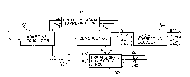
Referrlng to Flg. 5, the descrlptlon wlll proceed to
a demodulating system accordlng to a flrst embodlment of thls
lnventlon. The demodulatlng system ls for demodulatlng a 16-
QAM modulated slgnal produced by modulatlng a carrler slgnal
by four sequences of error-correctlng coded transmlsslon data.
The demodulatlng system lncludes an adaptlve equallzer 51
- 12 -
~'s
64768-237
2037~3~
whlch ls supplled wlth the modulated slgnal and ls for
adaptlvely equallzlng the modulated slgnal lnto an equalized
slgnal ln accordance wlth polarlty slgnals Dp and Dq and
corrected dlscrlmlnatlon error slgnals Ep' and Eq'. A
demodulator 52 demodulates the equallzed slgnal lnto
demodulated slgnals Sll, S12, S21, and S22 and dlscrlmlnatlon
error slgnals Ep and Eq. A polarlty slgnal supplylng unlt 53
supplles the polarlty blts Sll and S12 to the adaptlve
equallzer 51 as the polarlty slgnals Dp and Dq. An error-
correctlng decoder 54 produces error locatlon slgnals Spl,Sp2, Sql, and Sq2 representatlve of locatlons of errors ln the
data blts Sll, S12, S21, and S22. The error-correctlng
decoder 54 corrects the errors ln the demodulated slgnals by
uslng the error locatlon slgnals Spl, Sp2, Sql, and Sq2 lnto
decoded slgnals Sll', S12', S21', and S22'. An error slgnal
correctlng clrcult 55 ls connected to the demodulator 52 and
the error-correctlng decoder 54 and corrects the
dlscrlmlnatlon error slgnals Ep and Eq lnto corrected
dlscrlmlnatlon error slgnals Ep' and Eq' ln accordance wlth
the error locatlon slgnals Spl, Sp2, Sql, and Sq2. Corrected
dlscrlmlnatlon error slgnal supplylng llnes 56 are connected
to the adaptlve equallzer 51 and the error slgnal correctlng
decoder 54
"- 64768-237
2037S35
14
and supplies the corrected discrimination error signals
Ep' and Eq' to the adaptive equalizer 51.
Referring to Fig. 6, the error correcting
decoder 54 and the error signal correcting circuit 55
5 will be described more specifically. The error
correcting decoder 54 comprises error location detecting
circuits 541, 542, 543, and 544 for detecting the
locations of errors and producing the error location
signals Spl, Sp2, Sql, and Sq2. Such circuits are
10 described in Volume II of Elements of Digital Satellite
Communication written by William W. Wu and published
1985 by the Computer Science Press, Rockville, Maryland.
An error correcting and decoding circuit 545 includes
elastic memories (MEM) 546a, 546b, 546c, and 546d and
15 exclusive OR circuits (EORs) 547a, 547b, 547c, and 547d.
The elastic memories 546a, 546b, 546c, and 546d are for
giving the error-correcting coded data bits for a delay
time between reception of the demodulated signals Sll,
S12, S21, and S22 from the demodulator 52 and reception
20 of the error location signals Spl, Sp2, Sql, and Sq2
from the error location detecting circuits 541, 542,
543, and 544. The EORs 547a, 547b, 547c, and 547d
correct errors and output the decoded signals.
The error signal correcting circuit 55 comprises
25 correcting circuit delay circuits 61 and 62 for delaying
the error signals Ep and Eq by the delay time. The
correcting circuit delay circuits 61 and 62 thereby
produce delayed signals Ep" and Eq". Producing circuits
2037~35
67 and 68 lnclude OR clrcults 65 and 66 and excluslve OR
clrcults (EORs) 63 and 64. The OR clrcult 65 ls connected to
the error locatlon detectlng clrcults 541 and 543 and produces
an error locatlon slgnal Sp. The OR clrcult 66 is connected
to the error locatlon detectlng clrcults 542 and 544 and
produces another error locatlon slgnal Sq. The EOR 63 ls
connected to the delay clrcult 61 and the OR 65 and produces
the corrected error dlscrlmlnatlon slgnal Ep' ln accordance
wlth the delayed slgnal Ep" and the error locatlon slgnal Sp.
The EOR 64 ls connected to the delay clrcult 62 and the OR 66
and produces the corrected dlscrlmlnatlon error slgnal Eq' ln
accordance wlth the delayed slgnal Eq" and the error locatlon
slgnal Sq. The polarlty slgnal supplylng unlt 53 comprlses a
delay clrcult for delaylng Sll and S12 to output the polarlty
blts Dp and Dq by a common tlme lnterval whlch ls equal to the
delay tlme.
Referrlng to Flg. 7, the descrlptlon wlll proceed to
a dlfferent demodulatlng system accordlng to a second
embodlment of thls lnventlon.
The demodulatlng system ls for demodulatlng a
modulated slgnal produced by 16-QAM modulatlng a carrler
slgnal by four sequences of error correctlon coded
transmlsslon data. The demodulatlng system lncludes a
demodulator 71 for QAM demodulatlng the modulated slgnal lnto
demodulated slgnals. An adaptlve equallzer 72 adaptlvely
equallzes the demodulated slgnal lnto equallzed slgnals Sll,
S12, S21, and S22 and dlscrlmlnatlon error slgnals Ep and Eq
ln accordance wlth polarlty slgnals Dp and Dq and corrected
- 15 -
= 64768-237
2037~3~
dlscrlmlnatlon error slgnals Ep' and Eq'. A polarlty slgnal
supplylng unlt 73 supplies the polarlty blts of the
demodulated slgnals to the adaptlve equallzer 72 as the
polarlty slgnals Dp and Dq. An error correctlng decoder 74
produces error locatlon slgnals Spl, Sp2, Sql, and Sq2 by
using the error correctlng code bits of the equallzed slgnals
Sll, S12, S21, and S22. The error correctlng decoder 74
corrects errors ln the equalized slgnals Sll, S12, S21, and
S22 and decodes the equallzed slgnals Sll, S12, S21, and S22
by uslng the error locatlon slgnals lnto decoded slgnals Sll',
S12', S21', and S22'. The error locatlon slgnals are
representatlve of locatlon of errors ln the equallzed slgnals
Sll, S12, S21 and S22.
An error slgnal correctlng clrcult 75 ls connected
to the adaptlve equallzer 72 and the error correctlng decoder
74. The error slgnal correctlng clrcult 75 corrects the error
slgnals Ep and Eq lnto corrected dlscrlmlnatlon error slgnals
Ep' and Eq' ln accordance wlth the error locatlon slgnals.
The error slgnal correctlng clrcult 75 comprlses
correctlng clrcult delaylng clrcults ln the manner descrlbed
ln connectlon wlth Flg. 6. The correctlng clrcult delay
clrcults are for delaylng the error slgnals Ep and Eq by a
delay tlme whlch ls equal to a
64768-237
17 2037535
time interval between reception of the error signals Ep
and Eq from the adaptive equalizer 72 and reception of
the error location signals from the error correcting
decoder 74. The correcting circuit delaying circuits
5 thereby produce delayed signals. Like in Fig. 6,
producing circuits are connected to the correcting
circuit delay circuits and the error correcting decoder
54. The producing circuits produce the corrected
discrimination error signals in accordance with the
10 delayed signals and the error location signals.
The polarity signal supplying unit 73 comprises
a delaying circuit for delaying the polarity bits in
demodulated signals by a delay time interval which is
equal to the delay time.
While this invention has thus far been described
in conjunction with preferred embodiments thereof, it
will readily be possible for those skilled in the art to
put this invention into practice in various other
manners. For example, this invention is applicable also
20 to an automatic gain control (AGC) circuit, an automatic
phase control (APC) circuit, and an interference
compensation circuit.