Note: Descriptions are shown in the official language in which they were submitted.
2~3779~
-- 1 --
CONh~ ~ ASSEMBLY FOR PRINTED CIRCUIT BOARDS
The lnventlon relates to a connector assembly for a
printed clrcult board, comprlsing a flrst connector element
wlth a first houslng of lnsulatlng material and regularly
arranged male slgnal and ground contacts connectable to a
printed circuit board, and a second connector element with a
second housing of lnsulatlng materlal, sald second connector
element havlng a matlng slde, which can be lnserted into the
first housing, and with regularly arranged female signal and
ground contacts with a connectlon element, whlch female
contacts wlll contact the correspondlng male contacts when the
second houslng is recelved in the first housing.
Such connector assemblies are known ln various
embodiments. In the design of the known connector assemblies
attention has mainly been pald to the mechanical aspects of the
connector assembly, in particular with respect to the forces
required for mating and unmating the connector elements.
Attentlon was only pald to the electrlcal aspects in that one
almed at realizlng good reliable connectlons between the
contacts of both connector elements. With increasing speeds of
the digital signals to be transferred, i.e. decreasing rise
tlmes, the electrical performance of the contacts as a circult
element becomes lmportant. In the known connector assemblles,
problems occur wlth higher signal speeds wlth respect to cross-
talk between slgnal contacts, transmlssion losses, reflectlons
and ground bounce or switching noise. Desplte an optimal
distrlbutlon of the ground and slgnal contacts, these problems
cannot be elimlnated below rlse times of 0.6 ns ln the known
- 2 - 203779~
connector assemblies.
The invention aims to provide a connector assembly of
the above-mentioned type wherein the problems occurring at high
slgnal speeds in the known connector assemblies can be obviated
by making the connector elements ln such a manner that the
performance of the contacts as a circuit element can be
previously determined and said slgnal distortions are
minimized.
To this end the connector assembly according to the
invention is characterized in that said second connector
element is provided with a plurallty of outer conductors,
selected ones of said outer conductors substantially entirely
circumferentially enclosing at least one of said signal
contacts, and each of said outer conductors having contact
sprlng sections at opposite sldes of said outer conductor
adapted to contact the ground contacts ad~acent to the
corresponding signal contact of the first connector element.
In this manner it is obtained that with coupled
connector elements the signal contacts together with the
corresponding outer conductors each form more or less a
transmission line with a geometry, the dimensional parameters
of which can be determlned in such a manner that the electrlcal
re~uirements which are made on the connector assembly, are met.
Further lt is possible to prevlously make an e~ulvalent
electrical dlagram of the connector whlch can be used ln
designing the overall system in order to take account of the
electrical performance of the connector assembly from the
beglnnlng. This latter possibility is an important advantage
~,~
2037798
-- 3
as at hlgh bit rates an interactlon occurs between the
connector and the surrounding connectlon elements of the
system, whereby the operation of the overall system ls
affected. Wlth the connector assembly according to the
invention it ls now possible to obtain an optimal operatlon
despite this interactlon.
Further the connector assembly accordlng to the
inventlon shows the advantage that the connector elements and
the male and female contacts can be made in a usual manner so
that all known design and manufacturing techniques of the usual
connector assemblles can be used advantageously. The
connection between the male and female contacts ls comparable
wlth the same of the known connector assemblles so that the
favourable mechanical properties thereof, such as
mating/unmatlng forces and ln partlcular the tolerances wlth
respect to the mutual posltlons of the contacts are malntalned
when used in rack and panel conflguratlons. Further all
contacts and outer connectors can be manufactured from metal
strips by stamping and formlng so that the manufacturlng costs
0 of the connector assembly accordlng to the lnventlon are low.
Preferably each slgnal contact of the second
connector element ls mounted ln the correspondlng outer
conductor by means of a dlelectrlc lnsert. In thls manner a
rellable mountlng of the signal contact in the corresponding
outer conductor ls reallzed. The lmpedance of each slgnal
contact can be determlned by using an lnsert wherein by
providing more or less recesses the dielectrlc constant of the
insert between the slgnal contact and the outer conductor can
~-- 20~779~
- 3a -
be determined. Thereby the combination of slgnal contact and
outer conductor which can be consldered as a transmlsslon llne,
can be provided wlth a desired impedance.
In another aspect of the present inventlon, there is
provlded a connector assembly comprlslng a flrst connector
element having a first housing with first signal and ground
contacts and a second connector element having a second housing
with second signal and ground contacts and a plurality of outer
conductors, the second connector element being removably
connected to the first connector element with the flrst signal
contacts contactlng the second slgnal contacts and at least
some of the first ground contacts contacting the second ground
contacts, each of the outer conductors substantially entlrely
circumferentlally encloslng at least one of the second contacts
and havlng contact sprlng sectlons at opposite sides of the
outer conductor contacting the flrst ground contacts located at
the opposite sldes of the outer conductor.
The inventlon wlll be further explalned by reference
to the drawlngs ln whlch some embodlments are schematlcally
shown.
Flg. 1 ls a section of a first embodiment of a
connector assembly whereln the first and second connector
elements are shown in a disassembled position.
Flg. 2 ls a sectlon correspondlng wlth flg. 1 of an
amended embodiment of the connector assembly according to the
inventlon.
,. ."~;~,~,
- 3b - 2~3~
Flg. 3 is a top view of the first connector element
of figs. 1 and 2.
Figs. 4a and 4b show perspective the ground contact
plates of the second connector element of flgs. 1 and 2,
respectively.
Fig. 5 is a partially shown perspective cut-away view
of the second connector element of the connector assembly of
fig. 1.
Flg. 6 is a section corresponding with fig. 1 of an
amended embodiment of the connector assembly according to the
invention.
Fig. 7 is a perspective view of an amended embodiment
of the outer conductor and corresponding signal contact as the
same can be used in the second connector element.
Fig. 8 is a partially shown perspective cut-away view
of an amended embodiment o~ the second connector element of a
connector assembly according to the invention.
Fig. 8a is a perspective view of an outer conductor
of the connector element of fig. 8 with dielectric insert.
Fig. 9 is a schematic section of the connector
element of fig. 8 to explaln the ground connection.
~ 4 2037798
Fig. lo is a section corresponding with fig. 1 of an
amended embodiment of the connector assembly according to the
invention.
Fig. 11 is a perspective view of the outer conductors
5 of the second connector element of the connector assembly ac-
cording to fig. 10.
Fig. 12 is a perspective view of a ground contact of
the first connector element of the connector assembly accor-
ding to fig. 10.
Fig. 13 shows in perspective an outer conductor of
the second connector element with two female signal contacts.
Fig. 14 is a top view of an alternative embodiment of
the first connector element according to the invention.
Fig. 15 is a section according to the line XV-XV of
15 fig. 14.
Fig. 16 is a perspective view of an outer conductor
with signal contact of the first connector element of fig. 14.
Fig. 17 is a section corresponding with fig. 15 of a
first connector element with amended connection to a printed
20 circuit board.
Fig. 18 shows in perspective the outer conductors
with signal contacts of the connector element of fig. 17.
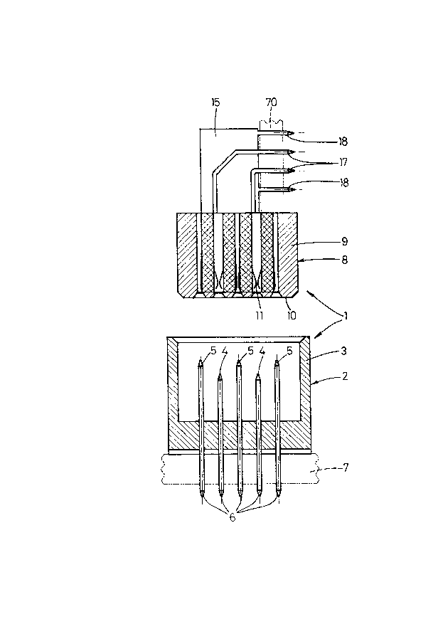
Referring to fig. 1 there is shown a cross-section of
a connector assembly 1 comprising a first connector element 2
25 with a first housing 3 of insulating material and contact pins
4 and 5 arranged in parallel rows r and columns c (see fig.
3). These contact pins 4, 5 each have a connection element 6,
by which the contact pins 4, 5 can be connected with the pla-
ted inner wall of holes in a printed circuit board 7 indicated
30 by a dashed. To this end the connection elements 6 are prefe-
rably provided with a known press-fit portion not further
shown.
As indicated in figs. 1 and 3, the connector element
2 comprises two rows with signal contact pins 4 which are in-
35 dicated by an s, wherein at both sides of each row with onlysignal contact pins 4 a row with only ground contact pins 5
indicated by a g is provided. The arrangement is such that a
column with only ground contact pins 5 is provided on both
sides of each column c with alternatingly signal contact pins
40 4 and ground contact pins 5. The rows with contact pins 4, 5
5 203779~
have a fixed intermediate spacing of 2mm, while in row direc-
tion the ground contact pins 5 lie at a fixed intermediate
spacing of 2mm and the signal contact pins 4 lie at a fixed
intermediate spacing of 4mm.
The connector assembly 1 is further provided with a
second connector element 8 with a second housing 9 of insula-
ting material adapted to be inserted with a mating side 10 in
the first housing 3 of the connector element 2. The second
connector element 8 is shown in perspective in fig. 5 and in-
10 cludes two rows with female signal contacts 11 for contacting
the signal contact pins 4 when the second housing 9 is recei-
ved in the first housing 3. Each signal contact 11 is enclosed
by an outer conductor 12 which seen in column direction has
opposite contact springs 13. In mated position these contact
15 springs 13 contact the ground contact pins 5 of the first con-
nector element 2 lying in the same column as the correspon-
ding signal contact pin 4.
Seen in row direction the outer conductors 12 have
opposite contact tongues 14 adapted to contact ground contact
20 plates 15 located on both sides of each outer conductor 12 in
the second housing 9. The contact tongues 14 lying at the ma-
ting side in fig. 5 conduct the current to the inner side of
the outer conductor 12 whereas the contact tongues 14 lying at
the other end conduct the current from the inner side of the
25 outer conductor to the ground contact plates 15.
Fig. 4a shows one ground contact plate 15 in perspec-
tive. This ground contact plate 15 is provided with female
contact elements 16 at the mating side, which contact elements
16 cooperate with the columns with only ground contact pins 5
30 of the first connector element 2. In this manner a very good
ground connection between both connector elements 2, 8 is ob-
tained, wherein a favourable current distribution in the outer
conductors 12 occurs.
Opposite of the mating side the ground contact plates
35 15 extend beyond the connection elements 17 of the signal con-
tacts 11. At these sides the ground contact plates 15 have
connection elements 18 for connection to a printed circuit
board 70 indicated with a dashed line in fig. 1. The connec-
tion elements 17 and 18 maybe provided with a press-fit por-
40 tion.
6 2037798
It is noted that the open space between each two suc-
ceeding ground contact plates 15 can be closed by providing a
ground contact plate 15 with extensions which extend from this
ground contact plate 15 to the adjacent ground contact plate
5 15. Thereby the signal contacts 11 will be fully enclosed by
ground contact plates.
Due to the fact that the signal contacts 11 are sur-
rounded by the outer conductors 12 and are further enclosed
between the ground contact plates 15, the signal contacts 11
10 with the outer conductor 12/ground contact plates 15 form a
transmission line with a geometry, of which the electrical
parameters and thereby the performance as circuit element can
be determined. The signal contacts 11 are mounted in the outer
conductors 12 by means of dielectric inserts 19. These dielec-
15 tric inserts 19 which can be manufactured by injection moldingat low costs, have a predetermined dielectric constant. By
providing larger or smaller recesses so that more or less air
is present between the signal contacts 11 and the outer con-
ductors 12, this dielectric constant can be determined and
20 thereby among others the impedance of the transmission line
formed by the signal contacts 11 and the outer conductors
12/ground contact plates 15. In this manner a connection can
be realized with a constant impedance, wherein cross-talk
between signal contacts cannot occur because each signal con-
25 ductor is surrounded by a ground conductor.
The connection elements 17, 18 of the signal contacts11 and the ground contact plates 15 may also be made as con-
tact springs adapted for surface mounting as appears from fig.
2, showing a connector assembly, the connector element 2 of
30 which fully corresponds with the connector element 2 of fig. 1
and the connector element 8 of which is provided with ground
contact plates 20 and signal contacts 11 adapted for surface
mounting. The connection elements are indicated by 17' and
18'. Fig. 4b shows in perspective a ground contact plate 20
35 used in the embodiment according to fig. 2.
Fig. 6 shows a cross-section of a connector assembly
21 mainly made in the same manner as the connector assembly
according to fig. 2. In this case however two rows of ground
contact pins 5 are mounted between the two rows of signal con-
40 tact pins 4. Ground cohtact plates 23 each having a contact
~ ~ 7 203~79~
spring 18' are used, which contact plates 23 can only contactthe ground contact pins 5 on both sides of the corresponding
signal contact pins 4. Thereby separated ground connections
for the two rows of signal contact pins 4 are obtained. Due to
5 the increased width of the connector assembly 21 it is also
possible to use a printed circuit board 22 with increased
thickness.
Fig. 7 shows in perspective one outer conductor 24
which can be mounted in the second connector element 8 for
10 connecting coaxial cables 25 to the printed circuit board 7.
The outer conductor 24 comprises a connection element 26 to
provide a simple connection with the outer conductor 27 of the
coaxial cable 25. To this end the connection element 26 is
first bent around the outer conductor 27. The signal contact
15 not further shown and mounted in the outer conductor 24 by the
dielectric insert 19, has a connection element 28 for connec-
ting the inner conductor 29 of the coaxial cable 25. The con-
nection between the outer conductor 27 and the inner conductor
29 can be obtained by soldering. After connecting the coaxial
20 cable 25 the parts 30 which are bent open and one of which is
not shown in fig. 7 for the sake of clearness, are closed.
Fig. 8 shows a perspective view of an amended embodi-
ment of the second connector element 8 with the housing 9,
wherein the outer conductors 12 at the side opposite of the
25 mating side 10 are provided with an extension 31 having two
ground contact pins 32 to be connected to a printed circuit
board 33. In fig. 8a one of the outer conductors with dielec-
tric insert 19 and both ground contact pins 32 is shown in
perspective. The ground contact pins 32 can be provided with a
30 press-fit portion. As appears from fig. 8a, the contact pins
32 are lying with respect to the longitudinal direction of the
outer conductor 12 diagonally with respect to each other.
Straight opposite of each contact pin 32 a recess 34 is provi-
ded, leaving free a hole 35 of the printed circuit board 33
35 which is intended to receive the ground contact pin 32 of an
adjacent outer conductor 12.
In the embodiment of the second connector element 8
according to fig. 8 it is possible to give each group of one
or more signal contacts a ground connection which is indepen-
40 dent of the same of other groups of signal contacts. Thereby
8 2~37798
a programmable lay-out of ground connections is possible. By
way of illustration fig. 9 schematically shows a section of
the housing 9 of the connector element 8, wherein for the sake
of clearness the outer conductors 12 and the inserts 19 are
5 not shown. In fig. 9 the signal contacts 11 are indicated by
an open rectangle, whereas the locations for the contact pins
4, 5 are indicated by shaded squares. In the second connector
element 8 according to fig. 8 ground contact plates 36 are
used which are separated for the,two rows of signal contact
10 pins 4 and which are indicated in fig. ~ by an oblique
shading. These ground contact plates 36 have only one female
contact element 16 which can only contact a corresponding
ground contact pin 5 of the outermost rows of ground contact
pins 5. In the embodiment shown insulating plates 37 (indica-
15 ted by a horizontal shading) are provided at three locationsin the housing 9 of the second connector element 8, while in
the middle row of ground contact pins 5 only one ground con-
tact pin 5 is mounted and four non-conductive insulating pins
38 (also horizontally shaded). Thereby the outer conductors lZ
20 of different groups of signal contact pins 4 and corresponding
female signal contacts 11 are insulated with respect to each
other, so that the ground connection of these groups is sepa-
rated and these groups cannot effect each other. By mounting
at suitable locations the insulation pins 3$ and insulating
25 plates 37 instead of ground contact plates 36 and ground con-
tact pins 5, each desired group of signal contacts with common
ground connection can be realized. It is noted that instead of
insulating pins 38 it is sufficiént just to omit the ground
contact pins 5 for separating the outer conductors 12 lying in
30 one column.
The ground contact plates 36 can also be coated on
one side with an insulating layer to obtain a separation be-
tween adjacent outer conductors 12. Thereby not only a sepa-
ration is possible but the outer conductor 12 lying at the
35 conductive side of the ground contact plate 36 maintains its
ground connection through this ground contact plate.
Fig. 10 shows a cross-section of a connector assembly
39, wherein the first connector element 40 mainly corresponds
with the first connector element~of fig. 1. In this case how-
40 ever the contact pins 4, 5 are located in column direction at
~ 9 2037~8
a mutual distance of 2,5mm. The signal contact pins 4 lie atan intermediate spacing of 4,5mm: Each three subsequent ground
contact pins 5 are united into a ground contact lip 41 shown
in fig. 12, which can have three connection elements 42 with a
5 mutual spacing of 1,5mm.
As appears from fig. 10, the connector assembly 39
comprises a second connector element 43 which in the same man-
ner as the second connector element 8 is provided with two
rows of female signal contacts. The second connector element
10 43 further comprises for each signal contact an outer conduc-
tor 44 and 45, respectively/ having an extension 46 and 47,
respectively. The outer conductors 44, 45 are perspectively
shown in fig. 11. The extensions 46, 47 have four connection
elements 48 which may be provided with a press-fit portion.
15 The outer conductors 44, 45 further have two contact springs
49 on both sides for contacting the ground contact lips 41
which are adjacent on both sides of the corresponding signal
contact pin 4 of the first connector element 40. Thereby the
ground connection is separated for each column of signal con-
20 tacts. If two rows of ground contact pins 5 are provided be-
tween both rows of signal contact pins 4 as in the embodiment
of fig. 6, each signal contact pin 4 can have a separated
ground connection.
Although not shown in fig. 11, each female signal
25 contact is mounted in the corresponding outer conductor 44, 45
also by means of a dielectric insert in the connector assembly
39. In fig. 10 two connection elements 50 of the female signal
contacts of the second connector element 43 are shown.
It is noted that in the embodiments of figs. 8 and 10
30 the signal contacts and the outer conductors of the second
connector element are provided with connection elements for
mounting in plated holes of a printed circuit board. Of cour-
se, also in these embodiments the connection elements can be
made as contact springs for surface mounting.
Although in the above-described embodiments of the
invention each female signal contact is enclosed by an outer
conductor, it is also possible to mount two or more signal
contacts within one outer conductor. Thereby twinax or triax
connections with the same favourable properties can be ob-
40 tained. The connector assembly according to the invention is
2037798
therefor for example also suitable for use in systems e~uiped
with ECL circuits.
Fig. 13 shows in perspeative as an example an outer
conductor 51 of a second connector element not shown, in which
5 two female signal contacts 52 are mounted by means of an in-
sert 53. The outer conductor 51 comprises ground connection
elements 54, whereas the signal contacts 52 each have a con-
nection element 55. Further the outer conductor 51 is provided
with contact springs 56 for contacting ground contacts of the
10 corresponding signal contact of the first connector element
not shown. It will be clear that both connector elements can
be made in the above-described manner for the remaining part.
The described connector assemblies already give a
substantial improvement as to the high frequency performance.
15 A further improvement can even be obtained if the signal con-
tacts of the first connector element are mounted in an outer
conductor in the same manner as the signal contacts of the
second connector element.
~igs. 14 and 15 show a top view and a section,
20 respectively, of a first connector element 56, wherein each
signal contact 4 is enclosed by an outer conductor 57 along
the portion of the signal contact extending in the insulating
material of the first housing 3. The signal contacts 4 are in
this case mounted in the outer conductor 57 by means of an
25 insert 58. It is noted that in this case also two or more sig-
nal contacts 4 can be enclosed by a common outer conductor 57.
The ground contacts 5 of the connector element 56
each comprise a plate-like portion 59 contacting the outer
conductor 57 of adjacent signal contacts 4. At the location of
30 the contact points the outer conductors 57 are provided with a
contact tongue 60 as shown in fig. 16.
In fig. 17 a section as in fig. 15 of a first connec-
tor element 61 is shown, which connector element 61 is adapted
for a perpendicular connection to a printed circuit board in-
35 dicated by a dashed line.
In this case the outer conductors 57 comprise anextension 62 which in the same manner as the extensions 31
of the outer conductors 12 is provided with ground connection
elements 63. In this case the ground contacts 5 are made
40 without connection elements 6. By way of illustration the
11 2~377g8
~. ~,
outer conductors 57 with extensions 62 are perspectively shown
in fig. 18. As appears from fig. 18, the connection elements
63 are provided in the same manner as the connection elements
32 of the extension 31 of the outer conductors 12. Also in
5 this case recesses 34 are made for the connection elements of
adjacent outer conductors. In fig. 18 the signal contact pins
4 with their connection elements 6 can also be seen.
It is noted that in the described embodiments of the
connector assembly according to the invention the first con-
10 nector element comprises rows of only signal contacts. It ishowever also possible to mount a ground contact between subse-
quent signal contacts. In that case the ground contact plates
of the corresponding second connector elements can be omitted
so that the ground contacts lying in a row of signal contacts
15 can directly contact the outer conductors through suitable
contact springs or the like.
In the first connector element 56 according to fig.
14 it is also possible to mount ground contacts between subse-
quent signal contacts.
Further it is noted that it is possible to use for
example U-shaped outer conductors, wherein the subse~uent
outer conductors join each other so that more or less closed
outer conductors are obtained.
The connector assembly according to the invention can
25 also be provided with signal contacts mounted in the usual
manner which of course are only suitable for relatively low
frequency signals.
From the above description it will be clear that the
invention provides a connector assembly wherein the signal
30 contacts with corresponding outer conductors can be considered
as a transmission line with such a geometry that the electri-
cal parameters of the connector assembly can be determined.
Thereby it is possible to adapt the impedance of the signal
contacts to the output impedance of the signal source and in-
35 put impedance of the receiver.
The connector assembly according to the describedembodiments of the invention provides a connection with a pre-
determined impedance between printed circuit boards or between
a printed circuit board and a multi-core cable. The manufac-
40 turing costs of this connector assembly are relatively low
~ 12 20377~8
because all signal and ground contacts and outer conductorscan be manufactured by stamping and forming. Further both
press-fit and surface mounting connections to printed circuit
boards are possible. The connection between male and female
5 contacts can be compared with the same of the known connector
assemblies so that the favourable mechanical properties there-
o~, like mating and unmating forces and in particular the to-
lerances with respect to the mutual positions of the contacts,
are maintained when used in rack and panel configurations.
The invention is not restricted to the above-
described embodiments which can be varied in a number of ways
within the scope of the following claims.