Note: Descriptions are shown in the official language in which they were submitted.
2~3~0~
PH~ ~0.~89 1 31.1.1991
DU~L PATH AMP~ITUDE MODUhATED RF AMPLIFIER
The invention relates to modulators and more
particularly to an amplitude modulated radio frequency
amplifier having dual path modulation ~or improved
operating efficiency.
Amplitude modulated radio frequency
amplifiers operating in the VHF an~ UHF frequencies
operate at a low efficiency. Current ~HF and U~F
- 10 transmitter RF power amplifiers are relatively poor in
converting primary DC power input to RF output energy
a~aila~le for communication. For mobile and portable
transmitters, the end result of the low efficiency is a
restrictive communications range and, for military
applications, a reduced immunity to int~rf2ring signals
(reduced jam margin~. Typically, conversion efficiencies
are less then 20%. ~rhis means that a radiaked 10 watt RF
carri~r power output signal requires a combined DC input
power and RF drive power of at least 50 watts to the
- transmitter final amplifier section. The 40 watts (or
more) that do not appear in the RF output power are lost
as heat within the output stage of the amplifier. Th~
inefficiency of the RF power ampli~ier not only
contributes a probl~m with excessive heat which must be
dissipated, but the generated heat also is involved with
an attendant reduction in reliability of the RF
amplifier r The associated DC power supply for operating
the amplifier must be of a sufficient size to supply the
wasted power, thereby ~ignificantly increasing the total
weight of the unit.
Because of the low operating efficiency of
the amplifier, there is a significant limitation on the
,
'
2~3~
PHA 40.589 2 31.1~19sl
available RF power output which can be produced from
limited capacity power source, such as a battery. By
limiting the RF power available for communications, the
communication range is limited and the transmitted
signal is more susceptible to jammingO On the other
hand, any increase in the available RF power achieved by
increased circuit efficiency will permit greater
communications distance and greater immunity to jamming
without an increase in power consumption. Or, an
improvement in power amplifier efficiency may be used to
achieve an increased battery life without a reduction in
the RF output power. Since an increase in eficiency
results in less heat generation, there also will be an
increase in equipment reliability and an opportunity to
reduce equipment weight.
The efficiency of an RF amplifier is
primarily determined by the power 105s in the active
device(s) used in the circuit, e.g., a power transistor
or a vacuum tube, and by the losses in the passive
circuit components, e.g., matching networks, filters,
etc. rhe power loss in an active device is primarily
determined by the instantaneous current through and the
instantaneous voltage across the device output element.
The active device drive signal characteristics usually
have a smaller impact on efficiency. Improvements in
operating efficiency usually come from improvements in
the characteristics of the instantaneous current through
and the instantaneous voltage across the active device
output element. These improvements are related to the
transfer character.istics of the device selected, and to
the operating point chosen for the device. The impact of
circuit configuration should be secondary in its impact
on efficiency. Howeverl practical considerations and
specialiæed designs often do cause the selected circuit
topology to influence the amplifier efficiency.
Normally, amplitude modulation for VH~/UHF
military transmitters is achieved by audio rate
2 ~
PHA 40.589 3 ~1.1.1991
variation of the RF drive signal ~envelope modulation of
the RF drive) for the power ~mplifier. Attempts have
been made to operate an RF power amplifier at a more
efficient operating point by modulating the DC power for
the
amplifier rather then the ~F drive. Early attempts at
output envelope modulation by power supply variation
have been found to lead to larg amounts of incidental
frequency modulation. The phy~ical separation of the
output amplifier from the low power RF drive system has
encouraged prior attempts at power supply modulation to
be performed only on the output amplifier. The RF drive
was operated at a predetermined level and was h~ld
constant while the output amplifier was modulated by
power supply variation~ The use of a constant RF drive
on the modulated amplifier causes a significant RF over-
drive during negative modulation peaks. Similarly, the
amplifier is significantly under-driven during positive
modulation peaks. This causes modulation transfer non-
linearity. The excess drive in the negative peaks tendsto be coupled into the output signal, but with a major
phase offset. The driva feedthrough phase of~sets, plus
the phase and propagation delay variations in the device
; as a result of supply modulation, creates a ~ignificant
angular modulation as a consequence of the supply
variation modulation technique and the RF overdrive.
Thus, prior power supply modulation efforts to obtain an
increased efficiency concentrated on a constant RF drive
to the power amplifier stage and experienced significant
incidental angular modulation. This discouraged the use
of efficient operatiny point control techniques.
It has been found that a dual path modulation
te~hnique may be used to alleviate much of the
detrimental effects previously noted in attempts to
improve RF power amplifier operating efficiency through
~3~
~HA 4~589 4 31.1.1991
power ~upply voltage modulation. Through the techniques,
both the power supply voltage to an RF power amplifier
and the RF drive to th~ amplifier are amplitude
modulated to achieve an e~ficient operating point for
the ampli~ier at all levels of modulation. Overall
performanc~ ~imilar to existing products is
obtainable with a significant increase in operating
effici~ncy. Prior art RF power ampli~iers driven by an
amplitude modulated RF drive ~ignal typically operate an
no more than 20% average efficiency. The actual
e~ficiency will vary with various factors including the
nature of the input signal used to modulate the RF drive
~e.g., sinusoidal waveform or square wave), the
percentage oP modulation, and the operating voltage for
the amplifier. Through the use of dual path modulation,
efficiency improvements for the RF output devices of up
to nearly double the present efficiency are obtainable.
According to the invention, an audio or other
low frequency input signal is used to modulat~ the DC
power supply voltage for operating an RF power
amplifier. The power supply voltage may be modulated by
various known techniques, for example, through the use
of a high ef~iciency pulse width modulator. The
amplitude modulated voltage is applied to the DC supply
input of the RF power ampli~ier and also is used to
amplitude modulate the RF drive signal applied ~o the
power ampliPier. Through the use of dual path ~power
supply and RF drive~ modulation, the amplifier can be
operated at the optimum efficiency operating point for
all levels of modulation. Through modulation of the RF
drive in addition to the power supply, prior art
problems with over-drive during negative modulation
peaks and underdrive during positive modulation peaks
can be elimi.nated. Finally, by using the voltage
modulated output from the power supply both for powering
the ampli~ier and for modulating the RF drive to the
amplifier, the possibility of phase shift distortion in
2 ~
pHa ~0.58~ 5 31.1.1991
the modulated output RF envelope of the a~plifier is
eliminated or minimi~edO
Ac~ordingly, it is an object of the invention
to provide an improved ef~iciency RF power a~plifier
through the use of dual path modulation.
Other objects and advantages of the invPntion
will be apparent from the following de~cription and the
accompanying drawings.
Fig. 1 is a graph showing efficiency vs.
output power for an exemplary prior art RF drive
modulated RF power amplifier for various power supply
voltages and showing by a dashed line a possible
ef~iciency vs. output power for the same amplifier
operated with dual path amplitude modulation according
to the invention;
Fig. 2 is a block diagram of ~ transmitter
having a dual path amplitude modulated RF amplifier
according to the invention; and
FigO 3 is a schematic circuit diagram of the
pulse width modulator and related filters for amplitude
modulating the DC power for thP RF amplifier of Fig. 2
and of the mixer connections for amplitude modulating
the RF drive for the amplifier.
The output power and total operating
effici~ncy for an RF power amplifier are determined by
various factors, including supply voltage and operating
point. In order to better understand the operation of an
exemplary RF power amplifier, Fig. 1 is a graph
illuskrating a family of operating point curves for
various DC power supply voltages for the amplifier when
operated at 225 ~Hz. ~he information on the graph is
plotted to show total efficiency as a function of RF
output power, with RF drive power and DC supply voltage
~3~
PHA 40.58~ 6 31.1.1991
as parameters of variation to generate a family of
curves. ~ach solid curve is plotted to represent a line
o~ operating points for the ampli~ier for increasing RF
drive at a specified DC primary supply voltage to the RF
power amplifier. For any given DC supply voltage to the
amplifier, thQ curve show~ an increa~e in both output
power and total efficiency with an increase in the RF
drive. For any given operating point ~or the amplifier,
-~ the total e~ficiency of the amplifier is calculated by
the following formulao
RF Output Power
Total Efficiency =
RF Input Power ~ DC Input Powe:r
A curve 10 in Fig. 1 shows the family of
operating points for the RF power amplifier when
operated from a 27 volts primary DC powPr supply. Other
exemplary curves are shown for the indicated lower
primary DC power supply voltage. The point A on the
curve lo may represent the amplifier operating point
when the RF input is a constant carrier at a level
s~lected to provide 10 watt6 of output power from the RF
amplifier. The point B on the curve 10 may represent 50%
positive peak modulation of the carrier by a 1 KHz sine
wave input signal and the point C may represent 100~
positive peak modulation of the carrier. The point D on
the curve 10 may represent 50~ negative peak modulation
of the carrier. Typically, a decrease in the DC
operatiny voltage for the ampli~iPr with a constant RF
drive will result in a decrease in the output power and
either substantially the same or a higher operating
ef~iciency for the amplifier.
The dashed line curve 11 represents the
operating points and resulting e~ficiency increases
which are obtainable through the use of dual path
modulation according to the invention. With dual path
modulation, any change in the magnitude of the input
signal will result in a corresponding chanye both in the
2~3~
PHA 40.5~9 7 31.1.1991
magnitude of the DC operating voltage for the amplifier
and in the operating point on the operating ~oltage
curve. A pure unmodulated carrier ma~ have an operating
point A', a 50% positive peak modulated carrier may have
an operating point B', a 100% positive peak modulated
carrier may have an operating point C' and a 50%
negative peak modulated carrier may have an operating
point D'. As will be seen from the exemplary curve 11,
~he DC voltage applied to the amplifier may be at about
22 volts ~or 100% positive peak modulation~ 15 volts for
50% positive peak modulation, 12 volts for the
u~modulated carrier and 9 volts for 50% negative peak
modulationO Of course, the actual operating points for
each level of modulation for maximum efficiency must be
determined for each specific amplifier circuit and
components. From comparing the exemplary curve 11 with
any of the fixed voltage curves on the graph of Fig~ 1,
it will be appreciated that. a significant increase in
efficiency at higher RF output power may be obtained
through the use of dual path modulation.
Turning now to Fig. 2, a block diagram is
shown for a co~nunications transmitter 12 having dual
path amplitude modulation of an RF power amplifier 13 in
accordance with the invention. For the following
discussion, the amplifier 13 is the ~inal output stage
in the transmitter 12. However, it will be appreciated
that the RF power amplifier 13 may be used for other
applications which will be apparent to those skilled in
the art. The transmitter 12 is operated from a suitable
primary DC power source 15, such as a battery (not
shown).
The trallsmitter 12 includes a conventlonal RF
carrier drive signal generator 16, such as a crystal
controlled oscillator or a frequency synthesizer and
appropriate amplifier stages. The transmitter 12 furtller
is connected to a conventional source 17 for an input
signal which must be communicated, in this case an audio
'
~3~
PH~ ~0.589 8 31.1.1991
signal source. The audio ~ignal source, for example, may
comprise a microphone and an audio amplifier. Of course,
the audio signal source may consist of other known types
o~ analog or digital signal ~ources which operate in the
low or audio freguency range.
T~e fixed voltage output from the primary DC
power source 15 is modulated with the audio signal ~rom
the source 17 and is applied to the RF power amplifier
: 13 as a source of operating power. This may be achieved
through the use of a DC voltage modulator, such as a
pulse width modulator lB and appropriate filters. Note
that although various DC modul tors will operate in the
dual path modulator of the invention with improvemPnts
in the efficiency of the RF amplifier, the use of a high
efficiency DC voltage modulator such as a high
~; e~iciency pulse width modulator will provide a total
improvement in the efficiency of the process of
obtaining a modulated voltage. The output voltage from
the source 15 is applied through an input filter 19 to
the pulse width modulator 18 and the audio output from
the source 17 is applied elther directly or, optionally,
through an overshoot filter 20 to the pulse width
modulator 18. The output from the pulse width modulator
18 is passed through a low pass filter 21 and applied as
a modulated DC voltage to a DC power supply input 22 to
the RF ampli~ier 13. The actual voltage operating range
for the amplifier 13 will depend on the operating
properties of each particular amplifier design and
particularly on the operating point efficiencies of the
active device(s) in the amplifier. For the amplifier
represented by the curve 11 in Fig. 1, the voltage
applied to the amplifier input 22 is modulated between
about 9 volts and about 22 volts. It is important to
prevent the DC supply voltage to the RF amplifier 13
from being modulated to too low of a value. If the DC
supply voltage drops too low, the junction capacitance
within the active device in the RF amplifier 13 will
2 ~
P~A ~0.589 9 31.1.1991
change and there will be excessive incidental phase
msdulation of the carrier signal. The negative envelope
peaks in the output ~rom the amplifier 13 should be
primarily obtained through RF drive modulation to reduce
incidental phase modulation.
The carrier from the RF drive signal
generator 16 and the modulated DC voltage from the low
pass filter 21 are applied to a modulator or mixer 23
which combine~ the modulated DC voltage and the carrier
lo to produce a modulated RF drive signal~ The transmit
carrier level of the drive signal is determined by an RF
leval control 24, which may consist o~ a manual level
adjustment. The RF drive signal from the mixer 23 ic
applied to an RF drive input 25 to the X~ amplifier 13.
Although the audio signal which is used to modlllate the
carrier may be obtained from other locations in the
transmitter circuit, it is preferable to use a small
portion of the modulated DC voltage from the low pass
filter 21 to amplitude modulate the carrier. ~his avoids
any phase differences in the modulated supply voltaye
and the modulated RF drive signal applied to the
amplifier 13, which would result in distortion in the RF
output from the amplifier 13. The mixer 23 may be
operated as a linear RF drive modulator. This will
result in some small sacrifice in the total ef~iciency
of the power amplifier 13. As will be discussed below,
maximum efficiency improvement is obtained with hoth
non-linear RF drive modulation and non-linear DC supply
voltage modulation. For any particular circuit design
for the amplifier 13, the maximum efficiency point must
be measured ~or various levels of modulation and such
measurements must be used in establishing the non-linear
drive modulation ~or optimum eff~ciency. It should be
noted that the modulation range of the supply voltage
applied to the amplifier 13 as well as the operating
characteristics of the amplifier 13 determine the
location and shape of the curve 11 in Fig. 1. The
.
2 ~
PHA 40.589 10 31.~.19
carrier level and the level of modulation of the RF
drive signal applied to the amplifier input 25 will
determine the operating point of the amplifier 13 on the
curve 11.
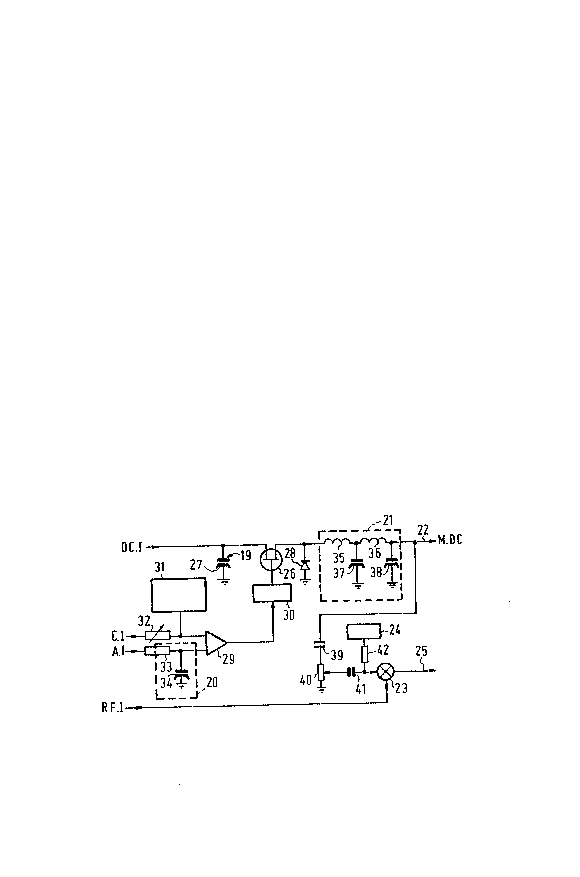
Fiq. 3 is a circuit diagram ~or the pulse
width modulator 18 and the related input filter 19,
overshoot filter 20 and low pass filter 21 and of the
connections for the RF drive modulatQr 23 from Fig. 2.
The pulse width modulator 18 (Fig. 2) has an output
voltage equal to the duty cycle of the switching
frequency times the DC voltage of the primary source 15
(Fig. 2~. Preferably, a power MOSFET 26 is used as the
switch because of its low "on" resistance and high speed
switching capabilities. ~he constant DC voltage from the
primary source 15 (Fig. 2) is applied to the source
electrode of the MOSFET 26. A capacitor 27 is also
connected between the source electrode and ground to
serve as the input filter 19. The drain electrode of th~
~OSFET 26 is connected through a diode 28 to ground and
to the low pass filter 21.
A comparator 29 has a pulse output which is
applied through a driver 30 to the gate electrode of the
MOSFET 26 for turning the MOSFET 26 on and off. The
comparator 29 compares an input ~rom a function
generator 31 with the audio signal ~rom the source 17
(Fig. 2). The function g~nerator 31 generates a high
frequency triangular waveform, for example, at a
frequency of approximately 200 KHz. A control input is
connected through a resistor 32 to add an adjustable DC
offset voltage to the output from the function generator
31. Note that the output impedance of the function
generator 31 must be compatible with the selection of
the resistance value for the resistor 32 in order to
provide a reasonable current summation effect at the
input to the comparator 29. In selecting the frequency
for the function generator 31, the design of the low
pass filter 21 should be considered. The audio signal
~3~
P~A 40.5~9 11 31.~.1991
~rom the source 17 (Fiy . 2 ) is applied to the comparator
29 through the overshoot ~ilter 20 which is a low pass
filter consisting of a series resistor 33 and a
capacitor 34 connected to ground. The duty cycle of the
puls~ train output of the comparator 29 determines the
operating point of the pulse width modulator 18. A fixed
change in t~e duty cycle of the resultant pulse train
may be caused by changing the level o~ the DC control
input. It is added as a DC of~set to the pulse train
from the function generator 31. The audio input to the
compaxator 29 creates a variable change (at the audio
rate) in the duty cycle of the comparator 29. As a
consequence~ the ~OSFET 26 will also have a variable
(audio) duty cycle pulse output at the switching
fre~uency of the function generator 31. This pulse
signal is smoothed into a modulated DC voltage by the
filter 21.
A further variable change may be made by
controlling the operation of the comparator 29 at its
audio input in response to the voltage level of the
primary DC power source 15 input to the pulse width
modulator. By varying the DC offset of the audio input,
the pulse width modulator 18 behaves as a "bucking" type
regulated power supply in addition to all other tasks it
performs. Changes in the voltage of the primary DC power
~ource are corrected by counter-acting changes in the
pulse width of the pulse width modulator output. This
helps maintain the average value of the supply voltage
to the RF amplifier at the target optimum value for
maximum RF amplifier efficiency.
The low pass filter 21 is a 4 element filter
consisting of two inductors 35 and 36 and two capacitors
37 and 38. The low pass filter 21 eliminates spikes
which would appear as spurious sideband signals on the
~5 transmitted RF signal. Where the function generator 31
operates at a frequency of 200 KHz~ a low pass filter 21
having a 3 dB rollo~f point at approximately 19 KHz and
2~3~
PXA 40.589 12 31.1~1991
a response o~ approximately -80 dB at 200 ICHz was
effective. The diode 28 provides a path for rever~e
currents from the ~ilter 21 when the ~OSFET 26 is
switched off. The optional over~hoot filter 20 is
provided tv compensate for the overshoot characteristics
of the 4 element low pass filter 21. The overshoot
filter 20 is requirRd only where the modulation
overshoot and ringing performance i~ tightly specified.
The modulator 23 may be an amplitude
modulator of known design. Where linear modulation is
desired, the modulator 23 may be a commercially
available frequency mixer, such as a model ZAD l
frequency mixer manufactured and sold by Mini-Circuits
of Brooklyn, New York. The modulated DC output from the
low pass filter 21 is connected through a series
capaoitor 39 and potentiometer 40 to ground. The tap on
the potentiometer 40 is connected through a ~apacitor 41
to the low frequency input to the mixer 23 and the RF
drive input is applied to an RF input to the mixer 23.
If the audio input to the mixer 23 has a zero volt
reference, the mixer 23 will produc~ a carrier
suppressed doubls sideband RF output. A DC unbalancing
circuit is required to deliver a carrier to the power
amplifier 13. The RF level control 24 merely consists of
an adju~table low voltage DC power supply with a series
resistor 42. The low voltage current is summed with the
audio signal at the input port to the mixer 23. The DC
serves to unbalance the input port o~ the mixer 23, thus
reducing the input balance and creatiny a carrier signal
at the RF port. Increasing the DC control signal will
increase the level o~ the carrie.r applied to the RF
power ampli~ier input 25. The adjustment of the RF level
by use of the DC offset also requires ths level of the
applied audio signal to be adjusted in order to obtain
the desired degree of envelope modulation. The
modulation level is adjusted by the potentiometer 40.
The degree of modulation obtained from the RF
~Q3~
PHA 40.~9 13 31.1.lg9
amplifier is usually greater than the modulation
variations o~ either the supply or the RF drive viewed
alone. The combination of the two modulation paths
provides an overall greater output modulation than
either path alone. The maximum efficiency improvement
results from a non-linear supply variation and an
associated non-linear RF drive variation. It should be
apparent from Fig 1 that the maximum efficie~cy will be
realized with primarily supply modulation and some drive
modulation providing the positive envelope ~odulation
and a primarily non-linear RF drive modulation providing
the negative envelope modulation. The use of primarily
RF drive modulation for the deep negative modulation
will reduce the amount of incidental phase modulation
1~ experienced, while having ~ nearly inconsequential
effect on total efficiency of the RF amplifier.
Although the dual path amplitude modulated RF
amplifier of the invention has been described and
incorporated in an audio signal transmitter, it will be
appreciated that the invention is suitable ~or other
applications. The RF amplifier is equally applicable to
digital ~ignal transmitters and to applications other
than the final stage of a transmitter~ In the described
preferred embodiment of the invention, the voltage ~rom
the DC power source is amplitude modulated with a pulse
width modulator and appropriate filters and the RF drive
is modulated with a frequency mixer. In the broadest
aspects of the invention, other known types of DC and RF
modulators may be adapted to modulate the power supply
voltage and the RF drive, respectively~ Xt also should
be noted that the efficiency improvements will vary with
the overall RF power amplifier design. However,
significant improvements should be obtainable compared
to an RF amplifier that aurrently utilizes RF drive
control exclusively as a means of RF output power
control and amplitude modulation control It will be
appreciated that various other modifications and changes
PHA ~0.589 14
may be madle to the above described preferr~ad embodiment
of the invention without departirlg from the spirit and
th~ scope of the following claims.
: . :