Note: Descriptions are shown in the official language in which they were submitted.
203~1 ~2
74842-3
PROGRAMMABLE CONNECTOR
A portlon of the dlsclosure of thls patent document
contains material which is sub~ect to copyrlght protection. The
copyright owner has no ob~ection to the reproduction by anyone of
the patent docurnent or the patent disclosure, as it appears in the
Patent and Trademark Office patent files or records, but otherwise
reserves all copyright rlghts whatsoever.
Field Of The Invention
This invention relates to large lntegrated clrcuits,
more particularly to programmable logic devices.
Backqround
Prior art prograrnmable logic devices can perform diverse
logic functions. These functions include computing combinatorial
logic functions such as AND, NAND, XOR, as well as storing such
logic functions. Further, particular inputs can be selected from
multiple inputs to a chip. U.S. Patent 4,870,302 describes an
invention of Xilinx, Inc., assignee of the present invention, for
performing such functions. U.S. Patent 4,706,216 describes a
loglc element used by Xilinx, Inc. to generate loglc functlons.
Products made as described in the above two patents are general
2038 ~ 62
74842-3
and powerful, able to perform selectable logic functions of many
varlables and able to be reprogrammed by a user to change which
loglc functions are generated. Devlces made by Xillnx, Inc. are
described in "The Programmable Gate Array Data Book," avallable
from Xilinx, Inc., 2100 Logic Drive, San Jose, CA 95124.
In order to direct the signals around a loglc array chip
to a particular logic element which will perform the desired
functlon, it may be desired to buffer a signal before placlng lt
onto an interconnect llne. Thls ls partlcularly true of signals
coming from off the chip or going off the chip. U.S. Patent
4,855,619 discloses a structure for controlling placement of
slgnals from a plurallty of llnes onto another llne, with
buffering if the line is of sufficiently high capacitance to need
buffering. Signals placed onto this interconnect line may be
generated by a logic element of the type described in U.S. Patent
4,706,216.
Some slmple logic functions do not require the general
and powerful abilities of the configurable logic element descrlbed
in U.S. Patent 4,706,216. Further, such simple logic functions
might be used together with other more complex functions for whlch
the full ablllties of a configurable logic array chip are needed.
One such simple functlon is the AND function. To perform this
functlon qulckly, manufacturers provlde a wide wlred AND gate such
as shown ln Fig. 1. Suppose that each of the transistors is N-
channel and that the inputs I1-I3 to the function are applied
through inverters INV1-INV3 to the gates of transistors N1-N3
respectively. When any of transistors N1-N3 ls turned on by a low
2038 1 62
74842-3
lnput slgnal on Il, I2, or I3, lnterconnect llne IC wlll be pulled
to ground, generatlng a loglcal 0 output slgnal. Only when all
lnputs Il-I3 are high will all transistors Nl through N3 be off so
that resistor Rl can pull the lnterconnect line IC high to produce
a loglcal 1 output slgnal. Thus the slgnal on lnterconnect llne
IC ls the AND-functlon of the slgnals Il-I3.
Xlllnx, Inc. provldes a means of performlng such a
functlon ln a configurable loglc array chlp. A buffer usable for
such a purpose may be as shown ln Flg. 2 and descrlbed in U.S.
Patent 4,855,619. The clrcult of Fig. 2 can be programmed to
present a hlgh lmpedance to llne LLl when the value on llne Ll ls
hlgh and a low voltage when the value on llne Ll is low. A high
value ln memory cell M61 turns on N-
2a
20~8~62
1 channel transistor T61, placing the signal from line Ll onto
2 line L2. A low value in memory cell M41 turns on transistor
3 T42 and turns off transistor T41 placing the signal from
4 line Ll into inverter B41 which puts the complement of the
5 signal on line Ll onto the gate of transistor T32. Thus a
6 high value of Ll turns off transistor T32, presenting a high
7 impedance on line LLl whereas a low signal on Ll turns on
8 transistor T32 and is propagated through T32 to line LLl. A
g plurality of lines such as Ll and L3 can be connected this
10 way to line LLl, which in combination with resistor R62 can
11 generate the AND function.
12
13 While this more sophisticated wired-AND gate has many
14 advantages, there are still some occasions where further
15 flexibility is desirable. For example, in complex
16 information processing applications it is sometimes desired
17 to have more than one logical function of the same set of
18 variables available simultaneously. Additionally, if the
19 logic function of the complement of an input signal is
20 required, that input signal will first have to be routed to
21 a logic element where it will be invert~d.~ Then the
22 inverted signal will have to be routed back to line LLl
23 which will generate the AND function of the inverted input
24 signal and other signals. Generating the complement of an
25 input signal in this way has two disadvantages. Firstly, it
26 slows down the speed of information processing. Secondly,
27 it uses valuable resources in the interior of the chip which
28 could otherwise be available for performing more complex
29 functions.
3 SUMMARY OF THE INVENTION
32 According to the present invention, a circuit generates
33 at least one logic function from selected ones of a set of
signals, wherein the set of signals consists of a first
35 subset of signals and a second subset made up of the
complements of the signals in the first subset. The logic
function is generated without ustng general purpose l-ogic
resources. The output signal or signals are generated
2038 1 ~2
1 quickly, preferably in a physically small portion of a logic
2 array chip close to the edge of the chip.
3 For each of a group of input signals, the input signal,
4 the complement of that input signal, or neither value can be
5 used to control a transistor which applies a voltage or a
6 high impedance to an interconnect line which holds the
7 function. Transistors which, when on, apply a first voltage
8 to the interconnect line are controlled by a programmable
g interconnect. The programmable interconnect causes a
10 respective transistor to turn on either in response to a
11 high input signal, in response to a low input signal, or to
12 remain off in response to either value of the input
13 signal. The transistor, in turn, applies either the first
14 voltage, for example ground, or a high impedance to an
15 interconnect line on which the function is generated. Other
16 transistors (or similar control means) also apply either the
17 first voltage or a high impedance to the interconnect
18 line. Means for applying a second voltage, for example a
19 positive supply voltage, to the interconnect line only when
20 no transistor is applying the first voltage, for example a
21 pull-up resistor connecting the interconnect line to Vcc,
22 are also provided.
23 Thus the first voltage is present on the interconnect
24 line when any transistor is turned on, and the second
25 voltage is present on the interconnect line when no
26 transistor is turned on. Therefore, the interconnect line
27 carries the combinatorial function of the set of signals
28 selected by the means for programming.
29 In one embodiment, each programmable interconnect is
30 separately programmable to select between responding to a
31 signal, its complement, or neither.
32 In a wide function embodiment, a programmable
33 interconnect turns on a corresponding transistor in response
to a combinatorial function of a set of input signals. A
35 plurality of transistors, each controlled by a set of input
36 signals, is controlled to apply the first voltage to the
7 interconnect line. Thus a function of many input variables
38 may be provided without adding corresponding capacitance to
2038 1 62
74842-3
the interconnect llne.
A choice between the functlon generated on the
lnterconnect llne and the complement of the generated functlon can
be made by selectlng whether the generated functlon ls inverted
before being applied to an output llne.
When the flrst voltage source ls ground and the second
voltage source is the posltlve voltage supply, each lnterconnect
llne provldes the AND functlon of any selection of input slgnals
or thelr complements. The AND functlon can be programmed to be
independent of any particular input signal or lts cornplement. In
a preferred embodlment, the lnput and lnterconnect llnes are
avallable ln close proxlmity, so the length of the input and
lnterconnect llnes ls short and thelr capacitance small, thus
allowing stlll faster operating speed.
According to a broad aspect of the lnventlon there ls
provlded a programmable connector for a programmable logic device
comprlslng:
at least one I/O llne;
at least one lnterconnect llne;
at least one programmable lnterconnect correspondlng to one
of sald at least one I/O llne and one of sald at least one
lnterconnect line, each of sald at least one programmable
lnterconnect comprlslng:
means for applylng a flrst voltage to said interconnect line;
programmable control means for controlllng sald means for
applylng a flrst voltage, sald programmable control means being
programmable to at least a flrst state such that in said first
2 0 3 8 1 62 74842-3
state sald means for applylng a flrst voltage provldes sald flrst
voltage to said correspondlng lnterconnect llne in response to a
flrst slgnal on sald correspondlng I/0 llne and provldes a hl~h
lmpedance to sald correspondlng lnterconnect llne ln response to a
second slgnal on sald correspondln~ I/0 llne; and
rneans for provldlng a second voltage to each of sald at least
one lnterconnect llne on whlch there ls no flrst voltage belng
placed by any of sald mealls for applylng a flrst voltage: and
means for programmably applylng one of a slgnal present on
sald lnterconnect llne and the complement of sald slgnal present
on sald lnterconnect llne to one of sald at least one I/O llne
~ ccordlng to another broad aspect of the lnventlon there
ls provlded a programmable connector for a programmable loglc
devlce comprlslng,
a plurallty of lnput llnes~
at least one lnterconnect llne~
at least one programmable lnterconnect, each correspondlng to
one lnterconnect llne and correspondlng to a plurallty of
lndependent lnput slgnals, each of sald at least one programmable
0 lnterconnect cornprlslng:
rneans for applylng a flrst voltage to sald lnterconnect llne~
prograrnmable control rneans for controlllng sald means for
applylng a flrst voltage, sald programmable control means belng
controlled by a prograrnmable set of sald lndependent lnput slgnals
such that sald means for applylng sald flrst voltage can be caused
to apply sald flrst voltage ln response to a selected cornblnatlon
5a
20 3 8 1 62
74842-3
of said lndependent lnput slgnals; and
means for provldlng a second voltage to each of said at least
one lnterconnect llne on whlch there ls no flrst voltage belng
placed by any of sald means for applylng a flrst voltage.
Accordlng to another broad aspect of the lnvention there
is provlded a programmable connector for a programmable logic
device comprlsing:
at least one I/0 line;
at least one interconnect llne;
means for segmenting at least one of said at least one
lnterconnect line comprislng at least one controllable swltchlng
means located along said at least one lnterconnect llne;
at least one programable lnterconnect correspondlng to one of
sald at least one I/0 llne and one of sald at least one
lnterconnect llne, each of sald at least one programmable
lnterconnect comprlslng:
means for applylng a flrst voltage to sald lnterconnect llne,
and
programmable control means for controlllng sald means for
applylng a flrst voltage, sald programmable control means belng
programmable to at least a flrst state such that ln sald flrst
state sald means for applylng a flrst voltage provldes sald flrst
voltage to said correspondlng interconnect line ln response to a
flrst signal on said correspondlng I/0 line; and provldes a high
impedance to sald correspondlng lnterconnect llne ln response to a
second slgnal on said corresponding I/0 llne; and
means for providing a second voltage to each of said at least
5b
,~
2038 1 62
74842-3
one lnterconnect llne on whlch there ls no flrst voltage belng
placed by any of sald means for applylng a flrst voltage.
Accordlng to another broad aspect of the lnventlon there
ls provlded a programmable connector for a prograrnmable loglc
devlce comprlslng:
at least one I/O llne;
at least one lnterconnect llne;
at least one programmable lnterconnect correspondlng to one
of sald at least one I/O llne and one of sald at least one
lnterconnect line, each of sald at least one programmable
lnterconnect comprlslng
means for applylng a flrst voltage to sald lnterconnect llne,
and
programmable control means for controlllng sald means for
applylng a flrst voltage, sald programmable control means belng
programmable to at least a flrst state such that ln sald flrst
state sald means for applylng a flrst voltage provldes sald flrst
voltage to sald correspondlng interconnect llne ln response to a
flrst slgnal on sald correspondlng I/O llne and provldes a hlgh
impedance to sald correspondlng lnterconnect llne ln response to a
second slgnal on sald correspondlng I/O llne; and
a latch lnserted between sald I/O llne and sald programmable
lnterconnect, sald latch comprlslng a data port connected to said
I/O line, an enable port, and an output port connected to said
programmable lnterconnect, sald output port belng connected to
said I/O line when a slgnal on sald enable port has a first state
and sald output port belng dlsconnected from sald I/0 llne when a
5c
A
20381 62
74842-3
slgnal on said enable port a second state, said output port
providing to said programmable interconnect a signal related to a
signal present on sald I/O llne when sald slgnal on said enable
port last had sald flrst state; and
means for provldlng a second voltage to each of sald at least
one lnterconnect llne on whlch there ls no flrst voltage belng
placed by any of sald means for applylng a flrst voltage.
Accordlng to another broad aspect of the lnventlon there
is provlded a programmable connector for a programmable loglc
devlce cornprlslng:
a plurallty of I/O llnes;
at least one lnterconnect line;
a plurallty of programmable interconnects, each corresponding
to at least one of sald I/O llnes and one lnterconnect llne, each
of sald programmable lnterconnects comprlslng:
means for applylng a flrst. voltage to sald lnterconnect line;
control means for controlling said means for applylng a first
voltage, said control means being controlled by a signal on said
at least one I/O llne,
means for programmably applylng a slgnal present on one of
sald at least one lnterconnect line to one of said plurality of
I/O lines, and
means for programmably applying the complement of said signal
present on said one of said at least one interconnect line to said
one of sald plurallty of I/0 llnes; and
means for providing a second voltage to each of said at least
one lnterconnect llne on whlch there ls no flrst voltage belng
5d
,, ~,
20381 62 74842-3
placed by any of said means for applylng a first voltage.
Accordlng to another broad aspect of the lnventlon there
ls provlded a programmable connector for an lntegrated clrcult
comprlslng:
a plurallty of I/O llnes;
at least one lnterconnect llne;
a plurallty of programmable lnterconnects, each of whlch
corresponds to one of sald I/O llnes and one of sald at least one
lnterconnect llne;
means for operatlng sald at least one programmable
lnterconnect in one of three modes, comprlslng:
means for, ln a flrst mode, provldlng a hlgh lmpedance to
sald correspondlng lnterconnect llne ln response to a hlgh slgnal
on sald correspondlng I/O llne, and provldlng a flrst constant
voltage to sald correspondlng lnterconnect llne ln response to a
low slgnal on sald correspondlng I/O llne;
means for, ln a second mode, provldlng a hlgh lmpedance to
sald correspondlng lnterconnect llne ln response to a low slgnal
on sald correspondlng I/O llne, and provldlng sald flrst constant
voltage to sald correspondlng lnterconnect llne ln response to a
hlgh slgnal on sald correspondlng I/O llne; and
means for, ln a thlrd mode, provldlng one of a slgnal present
on one of sald at least one lnterconnect llne to one of sald
plurallty of I/O llnes, and the complement of sald slgnal present
on sald one of sald at least one lnterconnect llne to sald one of
sald plurallty of I/O llnes.
Accordlng to another broad aspect of the lnventlon there
5e
~'
20~ 62 74842-3
ls provlded a programmable connector for a programmable loglc
device comprlslng:
at least one I/0 llne;
at least one lnterconnect llne;
means for segmentlng at least one of sald at least one
interconnect llne comprislng at least one controllable switching
means located along said at least one interconnect llne;
at least one programmable interconnect, each corresponding to
at least one of said at least one I/0 line and one interconnect
llne, each of sald at least one programmable interconnect
comprising
means for applying a first voltage to said interconnect line;
control means for controlling said means for applying a first
voltage, said control means being controlled by a signal on said
at least one I/0 llne; and
means for provldlng a second voltage to each of said at least
one interconnect line on which there is no first voltage being
placed by any of said means for applying a first voltage.
According to another broad aspect of the invention there
is provided a programmable connector for a programmable logic
device comprislng:
at least one I/0 llne;
at least one interconnect line;
at least one programmable interconnect, each corresponding to
at least one of said at least one I/0 line and one interconnect
line, each of said at least one programmable interconnect
comprising:
5f
20 38 1 ~
74842-3
means for applylng a flrst voltage to sald interconnect line;
control means for controlllng sald means for applylng a flrst
voltage, sald control means belng controlled by a slgnal on sald
at least one I/O llne; and
means for provlding a second voltage to each of sald at least
one interconnect line on which there is no first voltage being
placed by any said means for applying a first voltage;
said programmable connector further comprising a latch
inserted between said I/O line and said programmable interconnect,
said latch comprising a data port connected to said I/O line, an
enable ~ort and an output port connected to said programmable
interconnect, sald output port belng connected to said I/O line
when a slgnal on sald enable port has a flrst state and sald
output port belng dlsconnected from sald I/O line when a signal on
said enable port has a second state, said output port providing to
said programmable interconnect a signal related to a signal
present on said I/O line when said signal on said enable port last
has said first state.
According to another broad aspect of the lnvention there
is provided a programmable connector for a programmable logic
device comprlslng:
at least one I/O llne;
at least one interconnect line;
means for segmentlng at least one of sald at least one
lnterconnect llne comprising at least one controllable switching
means located along sald at least one lnterconnect llne;
at least one programmable lnterconnect, each correspondlng to
5g
r ~
20381 62 74842-3
at least one of sald at least one I/O line and one lnterconnect
line, each of said at least one programmable interconnect
comprising:
an N-channel FET transistor having one current carrying
termlnal connected to said first voltage supply and another to
said interconnect line, control means for controlling said
transistor, comprising:
a NAND gate having an output terminal connected to said
control terminal of said transistor, and at least two input
terminals, each receiving input from an output termlnal of a
programmable logic gate,
one said programmable logic gate having an input terminal
connected to said I/O llne and another lnput termlnal connected to
a memory cell which determines whether said logic gate will pass a
signal from said I/O line to said NAND gate, and
another said programmable loglc gate having an lnput terminal
connected to recelve the complement of a slgnal on sald I/O line
and another input terminal connected to a memory cell which
determines whether said another loglc gate will pass said
complement of said slgnal from said I/O line to said NAND gate;
and
means for providlng a second voltage to each of sald at least
one lnterconnect llne on which there is no flrst voltage belng
placed by any of said means for applying a first voltage.
BRIEF DESCRIPTION OF THE DRAWINGS
Fig. 1 shows a prior art programmable decoder.
Fig. 2 shows a prior art implementation of a wlred AND
'. ~
20381 62 74842~3
gate.
Fig. 3 shows a schematlc representation of a
programmable connector of the present invention.
Flg. 4 shows one ernbodiment of the programmable
connector of the present invention.
Fig. 5 shows another embodiment of the programmable
connector of the present lnvention.
Fig. 6 shows yet another ernbodiment of the programmable
connector of the present lnvention.
Fig. 7 shows a symbolic representation of a data/address
demultlplexer using a latch wlth the programmable connector of the
present lnventlon.
Fig. 8 shows a bidirectional programmable connector of
the present lnventlon.
Flg. 9 shows another embodlment of a bldlrectional
programmable connector of the present lnventlon.
Flg. lOa shows a symbolic representation of a
programmable connector in which input and output lines are
provided.
A
2~152
1 Fig. 10b shows logic functions which can be generated by
2 the circuit of Fig. 10a.
3 Fig. 11 shows an embodiment of the programmable
4 connector especially useful for a high speed wide AND gate.
Fig. 12 represents the layout of the programmable
6 connector in an integrated circuit chip with the connector
7 located between the edge of the chip and logic elements
8 internal to the chip, and having connections to both
g internal and external points.
11 DETAILED DESCRIPTION
12 One embodiment of the invention is shown in Fig. 3. Two
13 input terminals ITl and IT2 and two interconnect lines C
14 and OD are shown. Each interconnect line is connected
15 through a pull-up resistor RC or RD to voltage source Vcc.
16 Each input line is connected by means of one programmable
17 interconnect to each of the interconnect lines C and OD.
18 Each programmable interconnect can use either the signal on
19 the input line or the complement of that signal, or neither,
20 for controlling whether a voltage is applied to the
21 interconnect line.
22 Fig. 4 shows one embodiment of a programmable
23 connector. This programmable connector provides means for
24 placing the signal carried by an input line I onto
25 interconnect line IC. The programmable connector also
26 provides means for effectively disconnecting input line I
27 from interconnect line IC by providing a high impedance
28 between the two lines. The interconnect line IC is provided
29 with a pull-up resistor tied to a constant voltage. Thus,
30 the circuit of Fig. 4 implements a programmable connector to
31 provide the AND function. That is, line IC is pulled high
32 if there are no low signals being placed on it, and it is
33 pulled down if there is even one low signal being placed on
34 it. Thus, programmable interconnect 1 is designed to
35 provide a high impedance to IC to represent-a high signal on
input line I, and a low signal to IC to represent a low
37 signal on input line I. If the signal carried on the input
line I is to be included in the AND function, memory cell Ml
~38~&~
1 is programmed to provide a low signal to input 2 of NOR gate
2 NORl. With input 2 forced low, NOR gate NORl will invert
3 the signal carried on input line I. When input line I
4 carries a low signal, NOR gate NORl will place a high signal
5 on the gate of transistor Tl thus turning it on, and pulling
6 interconnect line IC low. When input line I places a high
7 signal on input 1 of NOR gate NORl, NOR gate NORl will place
8 a low signal on the gate of transistor Tl. This turns Tl
9 off and provides high impedance between interconnect line IC
10 and input line I.
11 If the logic function generated on IC is to be
12 independent of the signal on I, then memory cell Ml is
13 programmed to provide a high signal to input 2 of NOR gate
14 NORl. This forces the output of NOR gate NORl low, which
15 forces transistor Tl off. When Tl is off, a high impedance
16 is provided between the interconnect line IC and the input
17 line I, which effectively disconnects the two lines, thus
18 making the logic function provided on IC independent of the
19 signal carried on input line I.
Programmable interconnect 1 of Fig. 4 provides means for
21 placing only the signal carried on inp~t line I~- and not the
22 complement of that signal, onto interconnect line IC. To
23 provide means for placing the complement of a signal as well
24 as the signal itself, onto an interconnect line, a
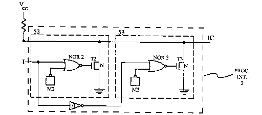
25 programmable interconnect 2 shown in Fig. 5 can be used.
2~ Programmable interconnect 2 provides two simple programmable
27 interconnects as shown in Fig. 4 cascaded together, where
28 the input signal is applied directly to NOR gate NOR2 and is
29 passed through inverter 10 before being applied to NOR gate
NOR3.
31 To control placement of a voltage onto interconnect line
3 IC in response to the signal carried by input line I, memory
cells M2 and M3 are programmed to ensure that section 52
turns on transistor T2 in response to a low signal on input
line I, and that section 53 maintains transistor T3 off
regardless of the signal on input line I. Memory cell M2 is
programmed to provide a low signal to NOR gate NOR2, which
allows NOR gate NOR2 to provide the complement of input I to
2038 1 62
1 transistor T2. A high signal at input I thus results in a
2 high impedance to IC to represent a high signal on input I
3 and a low signal to IC to represent a low signal on input
4 I. Memory cell M3 must be programmed to provide a high
5 signal to NOR gate NOR3, thereby forcing the output of NOR
6 gate NOR3 low and transistor T3 off regardless of the signal
7 on input I. This effectively disconnects section 53 of
8 programmable interconnect 2 from interconnect line IC.
9 If, however, a logical function of the complement of the
10 signal carried on input line I is required, then memory
11 cells M2 and M3 are programmed to turn section 53 on and
12 section 52 off. Memory cell M3 is programmed to provide a
13 low signal to NOR gate NOR3, which allows NOR gate NOR3 to
14 provide a low output in response to a low signal on input I,
15 in turn causing transistor T3 to provide a high impedance to
16 interconnect line IC (by turning T3 off) to represent the
17 low signal on input I. In this mode, NOR gate NOR3 will
18 cause transistor T3 to apply a low signal to interconnect
19 line IC (by turning T3 on) to represent a high signal on
20 input I. When memory cell M3 provides a low signal, memory
21 cell M2 must be programmed to provide a high signal to NOR
22 gate NOR2 regardless of the state of input I, thereby
23 forcing the output of NOR gate NOR2 low and transistor T2
24 off. This effectively disconnects section 52 of
25 programmable interconnect 2 from interconnect line IC.
26 If it is required that the signal on interconnect line
27 IC be independent of input signal I, then both of memory
28 cells M2 and M3 are programmed to provide high signals,
29 whereby transistors T2 and T3 provide high impedance to line
30 IC regardless of the state of input signal I.
31 A third programmable interconnect is shown in Fig. 6.
32 As does programmable interconnect 2, programmable
33 interconnect 3 provides means for placing either a signal or
34 its complement onto interconnect line IC. Also, like
programmable interconnect 2, programmable interconnect 3
provides a high impedance to IC to represent a high signal
(or a high complement signal) on input line I, and a low
signal (or low complement signal) to represent a low signal
20381 62
l on input line I. Programmable interconnect 3 is preferred,
2 however, because it adds less capacitance to interconnect
3 line IC than does programmable interconnect 2.
4 For the embodiment shown in Fig. 6, if an AND function
s of the input signal I is required, memory cell M5 iS
6 programmed to place a high signal on input 4 of OR gate OR5
7 and memory cell M4 iS programmed to place a low signal on
8 input 1 of OR gate OR4. This forces the output of OR gate
9 OR5 high, which in turn forces the input 20 of NAND gate
10 NANDl high. With input 20 forced high, the output of NAND
ll gate NANDl Will be determined by input 21, which receives
12 the output of OR gate OR4. Since memory cell M4 is
13 programmed to place a low signal on input l of OR gate OR4,
14 the output of OR gate OR4 follows the input signal placed by
lS input line I on input 2 of OR gate OR4. Since the output of
16 OR gate OR4 is the input 21 of NAND gate NANDl, the output
17 of NAND gate NANDl will be the complement of the signal on
18 input line I. Thus, for a high signal on input line I,
l9 transistor T4 will be turned off and a high impedance will
20 be provided to interconnect line IC. For a low signal on
21 input line I, transistor T4 will be turned on,~and
22 interconnect line IC will be pulled low.
23 If an AND function of the complement of the input signal
24 is required, memory cell M4 iS programmed to place a high
25 signal on input l of OR gate OR4 which forces the output of
26 OR gate OR4 high. This in turn forces the input 21 of NAND
27 gate NANDl high. With input 21 forced high, the output of
28 the NAND gate NANDl Will place the complement of the signal
29 on the other input 20 of the NAND gate onto the gate of
T4. Memory cell M5 iS programmed to place a low signal on
31 input 4 of OR gate OR5 so that the output of OR gate OR5
follows the complement of the input signal carried by input
line I, placed by inverter 20 on input 3 of OR gate OR5.
34 Since the output of OR gate OR5 iS the input 20 of NAND gate
NANDl, the output of NAND gate NANDl will turn transistor T4
off when input signal I is low, thereby providing a high
impedance to interconnect line IC. Likewise, NAND gate
NANDl turns on transistor T4 when input signal I is high,
203~ 1 ~2
1 thereby pulling down line IC. In this way the logic
2 function provided by interconnect line IC will be a function
3 of the complement of the signal on input line I.
4 Finally, if the function on interconnect line IC is to
5 be independent of the input signal I, memory cells M4 and M5
6 are programmed to provide high signals to gates 1 and 4 of
7 OR gates OR4 and OR5 respectively, thus applying high
8 signals to both of inputs 20 and 21 of NAND gate NANDl,
9 causing transistor T4 to be off regardless of the state of
10 inpu-t signal I.
11 The determination of a specific logic function will be
12 explained with reference to Fig. 3. Suppose that signal A
13 is placed on input terminal ITl and signal B is placed on
14 input terminal IT2. Further suppose that interconnect line
15 C is required to carry the function A AND B, and
16 interconnect line OD iS required to carry the function A.
17 To generate the function A AND B on interconnect line
18 C' programmable interconnect Cl and programmable
19 interconnect C2 must be appropriately programmed.
20 Programmable interconnect Cl is programmed (as discussed
21 above) to represent the input signal carried by input
22 terminal ITl on interconnect line C (i.e. high impedance
23 represents a high input signal; a low voltage represents a
24 low input signal). Programmable interconnect C2 is
25 programmed to represent the complement of the input signal
26 carried by input terminal IT2 to interconnect line C In
27 this way the interconnect line C will carry the logical
28 function A AND B-
29 To generate the function A on interconnect line OD,
30 programmable interconnect Dl is programmed to represent the
complement of the signal carried on input terminal ITl to
interconnect line OD. Programmable interconnect D2 is
programmed to effectively disconnect interconnect line OD
from input terminal IT2 so that the signal on OD will be
independent of both the signal and the complement on IT2.
In this way, the interconnect line OD will carry the logical
function A.
38 One application of the programmable connector of the
--10--
2038 1 62
1 present invention is for use with the data/address
2 demultiplexer shown in Fig. 7. Input line I carries a time
3 multiplexed signal which part of the time represents an
4 address, and part of the time represents data present at
5 that address. Input line I is connected to the input port D
6 of latch 31. An enable signal, typically generated off-
7 chip, is applied to the enable port E of latch 31. The
8 output port Q of latch 31 is connected to a programmable
9 interconnect Al. When the signal applied to enable port E
10 is high, the signal presented at input port D by input line
11 I is passed to the output port Q of latch 31. Programmable
12 interconnect Al then passes the signal on Q, or its
13 complement, or neither, to the interconnect line IC. This
14 signal is part of an address which will be sent to the
15 appropriate circuit element or set of circuit elements by
16 interconnect circuitry to which interconnect line IC may be
17 connected. While a particular value is latched into latch
18 31 (and typically other latches, not shown, which carry
19 other parts of the address), a certain device will be
20 enabled by the address. When the signal presented to E then
21 goes low, the address is latched into la~ch 31, and the data
22 on input line I (and other lines, not shown) which are
23 demultiplexed at latch 31 (and other latches, not shown) can
24 be sent to the addressed device (or to general interconnect
25 circuitry which will then route the signal to the addressed
26 device) by line 32 (and other data lines not shown).
27 In another embodiment using bi-directional programmable
28 interconnects, a single pin can be used as either an input
29 pin or an output pin.
Two examples of such bi-directional programmable
31 interconnects are shown in Figs. 8 and 9. The bi-
directional programmable interconnect shown in Fig. 8 is
structurally similar to the programmable interconnect 1
discussed earlier and shown in Fig. 4, except that the
35 bi-directional programmable interconnect contains an
additional memory cell M10 and an additional transistor
T10. Thesé two extra components of the bi-directional
programmable interconnect make it possible to pass a signal
--11--
2038 1 ~2
1 either from input/output line I/O to interconnect line IC,
2 or from the interconnect line IC to input/output line I/O or
3 for input/output line I/O to be disconnected from
4 interconnect line IC, and therefore independent of each
s other.
6 Thus for input/output line I/O to function as an output
7 line, node A is connected to the input/output line I/O by
8 programming memory cell M10 to turn transistor T10 on.
9 Further, Node C is effectively disconnected from
10 input/output line I/O by turning transistor Tll off.
11 Transistor Tll can be turned off by programming memory cell
12 Mll to place a high signal on input 51 which forces the
13 output of NOR-gate NOR50 low.
14 When input/output line I/O is functioning as an input
15 line, node C is used as discussed earlier. Node A is
16 disconnected from input/output line I/O by programming
17 memory cell M10 to turn transistor T10 off. Further, memory
18 cell Mll is programmed to place a low signal on input 51 so
19 that NOR gate NOR50 works exactly as NOR gate NORl does in
20 the programmable interconnect of Fig. 4.
21 A more sophisticated bi-directional;programmable
22 interconnect shown in Fig. 9 has three modes of operation.
23 In the first mode, input/output line I/O functions as an
24 output line, and the bi-directional programmable inter-
25 connect can pass a signal on an interconnect line or the
26 complement of a signal on an interconnect line to an I/O
27 line. In the second mode, input/output line I/O functions
28 as an input line, and the bi-directional programmable
29 interconnect can pass a signal on an I/O line or the
3 complement of a signal on an I/O line to an interconnect
31 line. In the third mode the bi-directional programmable
32 interconnect can effectively disconnect an interconnect line
33 from an I/O line by providing high impedance between the two
3 lines.
Operation in the first mode, that is, when input/output
line I/O is functioning as an output line, is as follows.
Node E is used for routing a signal from interconnect line
IC to line I/O. Node F is used to route the complement of
-12-
203~ 1 62
1 the signal on interconnect line IC to line I/O. Node D is
2 used in the input mode. For the output mode, node D is
3 disconnected from the interconnect line by programming both
4 memory cells M21 and M22 to place a high signal on inputs 61
5 and 62 of OR-gates 71 and 72, respectively. This forces the
6 outputs of these OR gates high, which in turn forces the
7 output of NAND gate 73 low, which turns off transistor
8 T20. If the signal on interconnect line IC is to be placed
9 onto input/output line I/O, then transistor T21 is turned on
10 by memory cell M23 and T22 iS turned off by memory cell
11 M24. This allows passage of the signal on the interconnect
12 line to input/output line I/O through transistor T21. If
13 the complement of the signal on interconnect line IC is to
14 be placed on input/output line I/O, then transistor T22 iS
15 turned on by memory cell M24 and T21 is turned off by memory
16 cell M23. This allows the signal on interconnect line IC to
17 be inverted by inverter 10 before being placed on
18 input/output line I/O.
19 Operation in the second mode, where input/output line
20 I/O is to function as an input line, is achieved by
21 disconnecting both nodes E and F from the interconnect
22 line. This can be done by programming memory cells M23 and
23 M24 to turn off transistors T21 and T22, respectively, by
24 placing a low signal on the gate of each transistor. Then,
25 memory cells M21 and M22 are programmed as were memory cells
26 M4 and MS in Fig. 6.
27 Operation in the third mode, where input/output line I/O
28 is independent of interconnect line IC, is achieved by
29 programming memory cells M21 and M22 to place high signals
30 on inputs to OR gates 71 and 72 and simultaneously
3 programming memory cells M23 and M24 to place low signals on
3 gates of transistors T21 and T22. With all three of
transistors T20, T21, and T22 off, the programmable
34 interconnect of Fig. 9 disconnects input/output line I/O
from interconnect line IC.
36 In addition, the bi-directional programmable
interconnect of Fig. 9 also allows the programmable
connector to generate additional logic functions. This is
-13-
1 because when the input/output line I/O functions as an
2 output line, the bi-directional programmable interconnect of
3 Fig. 9 provides means for placing either the signal or the
4 complement of the signal carried by interconnect line IC
5 onto input/output line I/O. This ensures a structure
6 parallel to the ordinary programmable interconnect wherein
7 the signal carried by the input line, or the complement of
8 that signal, can be placed onto the interconnect line. Fig.
9 10a shows a schematic representation of the circuit for
10 generating functions of input signals A and B and placing a
11 function of A and B onto output line OUT. Programmable
12 interconnects PIA and PIB may be dedicated input
13 interconnects as shown in Figs. 5 and 6 or bidirectional
14 interconnects such as shown in Fig. 9. Likewise,
15 programmable interconnect PIo may be bidirectional as shown
16 in Fig. 9 or may comprise only the output circuit elements
17 shown on the right side of Fig. 9. Fig. 10b represents the
18 set of functions which can be generated when the signal
19 present on interconnect line IC can be inverted before
20 applying to output line OUT. For the case where the signal
21 on interconnect line IC is generated from input signals A
22 and B, inverting of the output signal allows the following
23 additional functions to be provided: (A+B), (A+B), (A+B),
24 and (A+B). Moreover, these additional logic functions are
25 generated without using any of the more general purpose
26 logic resources located in the chip.
27 A further embodiment, shown in Fig. 11, allows
28 implementing a much wider AND-gate without adding
29 corresponding capacitance to interconnect line IC.
In the connector embodiment of Figs. 4, 6, and 9, each
31 input line required its own programmable interconnect. Each
32 programmable interconnect adds some parasitic capacitance to
33 the interconnect line IC. In the wider decoder of Fig. 11,
3 there can be several input lines using the same programmable
35 interconnect since the AND function of some subset of input
signals and complements is used by a NAND gate to generate
another AND gate input before reaching interconnect line
IC. Since fewer programmable interconnects are required,
CRP/M-1238-D 203 8 1 62
there is less capacitance added to the interconnect
2 line IC.
As shown in Fig. 11, different means for applying input
signals to interconnect line IC are used. Each of the input
lines Il - In is connected to an input of a NAND gate such
as NAND gate 11 by means of two memory cells, four pass
transistors, and one inverter arranged as shown in unit
U41. NAND gate 11 controls a transistor T41. Depending on
how memory cells M51 and M52 are programmed, either the
signal on input line Il or its complement can be input to
the NAND gate input terminal 41, or input line Il can be
effectively disconnected from NAND gate 11. Disconnecting
the input line Il is achieved by loading logical 0's into
memory cells M51 and M52, thereby turning off both of
transistors T63 and T64 and turning on transistors T61 and
T62, allowing a high signal to be passed to NAND gate 11
through transistors T61 and T62. In this way, the signal on
line Ll can be the AND function of any combination of the
signals or the complements of the signals on input lines
Il In.
221 Further, additional lines such as line ~n,-ea~h with
their own sets of input lines (not shown), can be connected
to interconnect line IC. Interconnect line IC will provide
the AND function of any combination of the signals or
complements of signals on all of the input lines such as Il-
In which in turn provide input to NAND gates for controlling
lines Ll~Ln
An embodiment shown in Fig. 12 illustrates several more
features of the invention. As shown in Fig. 12, the input
and interconnect lines are placed between the edge E of the
chip and logic blocks such as LOGIC 1 and LOGIC 2 interior
to the chip. This way, the delay a signal experiences, for
example, while traveling from input pins IPl and IP2 through
input/output buffers IOBl, IOB2, through programmable
interconnects such as Al to interconnect line OA2, is
36 minimized, thus minimizing capacitance and increasing the
speed of the circuit. Further, the signal on an
interconnect line OA, OB, OC or OD can easily be sent off
CRP/M-123~-D 2 0 3 8 1 6 2 PATENT
the chip by simply routing it to an appropriate output line
such as OUT and through an input/output buffer such as IOB3
to an output pin such as Pl.
The speed can also be improved by locating pass
transistors or transmission gates along the interconnect
lines OA, OB~ C and OD. For example, if the logic
functions of the signals on pins IPl and IP2 will be used at
LOGIC 2, then pass transistors or transmission gates T5-T8
controlled by memory cells M5-M8 are turned on so that the
signal on the selected interconnect lines OA2-OD2 will be
available to the switch matrix l interconnect leading to
LOGIC 2. In this case, pass transistors or transmission
gates Tl-T4 are turned off, effectively separating
interconnect line segments OAl, OBl~ Cl and ODl f
interConnect line segments OA2~ g2~ C2~ and OD2- If the
signal on an interconnect line is needed in close proximity
to the input lines, for example at LOGIC l or OUT, pass
transistors or transmission gates T5-T8 controlled by memory
cells M5-M8 can also be turned off, further decreasing the
length and thereby the capacitance of the interconnect lines
OA2-OD2, and consequently the switching~ime of th^e signal.
Provision of pass transistors or transmission gates such
as Tl-T8 to segment the interconnect lines allows one chip
to have a selectable number of separate decoders or other
programmable connectors located around the perimeter of the
chip. In order for each separable segment to operate as
discussed, a pull-up resistor is connected to every segment
of every interconnect line, as shown, so that each separate
segment can provide both high and low voltages as
required. For example resistor RDl is connected to segment
ODl, resistor RD2 is connected to segment OD2 and resistor
RD3 is connected to segment OD3.
In order for a segment to operate as an interconnect
line for transmitting a signal between I/O lines connected
to the interconnect line, and not to operate as a function
37 generator, some of the resistors, in this case resistors
38 RAl' RBl' RCl and RDl, shown in figure 12 are formed in
series with pass transistors, TAl, TBl, TCl and T
-16-
CRP/M-1238-D 2 0 3 8 1 6 2 PATENT
respectively. When a pass transistor is off, the
corresponding pullup resistor is disconnected, thus allowing
the interconnect line to pass a signal from one I/O line to
another I/O line. For example, turning off transistors T
and T4 allows line segment OAl to serve as an interconnect
line for input/output lines (not shown) connected to line
segment OAl. Also, if several segments are connected
together it may be desirable to connect only one resistor to
the connected set of line segments in order to save power,
or conversely to connect more than one resistor in order to
11
12 increase speed.
13 Further, the input signals can come either from input
pins such as IPl or IP2, or from circuitry in the interior
of the chip, for example from switch matrix l or logic
device LOGIC l. Similarly, the generated logical functions
can be sent directly to output pins such as Pl, or routed
to the general interconnect circuitry at the interior of the
chip.
It is within the scope of the present--invention to
programmably divide lines running along the perimeter of a
chip into any number of segments by using pass-transistors
23 or transmission gates to separate the segments. Likewise,
24 the invention may provide segments which do not extend
around the full perimeter, may provide segments within the
26 interior of a chip, and may provide segments which extend
27 from the perimeter to the interior of the chip. Any number
of interconnect lines may be provided. It is further within
the scope of the present invention to provide input lines
which can connect to less than all the lines crossed. Also,
not all input lines need have their complement signals
readily available to the interconnect lines It is further
within the scope of the invention to provide bi-directional
buffers so that input pins to which the buffers connect can
be used as either input or output pins. Further, it is
possible to implement other logic functions including OR,
NAND, and NOR, just as the AND function which has been
described, by changing the polarity of the voltages applied
to the interconnect line or by adding inverters.
~38~ ~2
~RP/ M- 12 3 8 -D PATENT
Further modifications will become obvious to those
skilled in the art in li~ht of the above disclosure and are
also intended to fall within the scope of the invention.
o
1 5
16
18
19
22o
2232
26
278
29
31
3343
36
38
--18--