Note: Descriptions are shown in the official language in which they were submitted.
-1- LD ~.0, 055
BALLAST CIRCUIT WITH IMPROVED TRANSFER FUNCTIONS
BACKGROUND OF THE INVENTION
The present invention relates to a power circuit
that supplies DC excitation to a gas discharge lamp.
More particularly, the present invention relates to a
ballast circuit that automatically and sequentially
provides desired transfer functions for the DC
operation of the metal halide lamp.
The ballast circuit having its desired transfer
functions provides the necessary voltage and current
conditions to the gas discharge lamp, such as a metal
halide lamp, so that it properly performs during its
various modes of operation which are: (1) an initial
high voltage breakdown or start mode; (2) a glaw-to-arc
transition or glow mode; and (3) a steady state, arc or
run mode. Each of these modes have different voltage
and current requirements allowing the gas discharge
lamp to perform in a proper manner. It is desired that
these various current and voltage requirements be
provided in an automatic and sequential manner so that
the lamp transitions from its start, to its glow, and
then to its run mode. Similarly, it is desired that
these voltage and current conditions be automatically
provided if the lamp reverts from its run mode to its
glow or start mode.
6) ~1 '.'.s < ~ .
s~ '~ cJ '~ ,~
-2- LD 10,055
The current developed by the ballast circuit which
flows through the gas discharge lamp may typically
experience surges as these lamps enter or revert from
its modes of operation, for example, as the lamp
ionizes and enters into the glow mode, the current
flowing at this entrance is of a relatively large value
and is of a relatively high rate of change which may be
such so as to detrimentally affect the associated
circuit components of ballast circuit and especially
the lamp itself. It is desired that a ballast circuit
be provided with means to limit the maximum amount of
current supplied to the lamp during its modes of
operation and also to limit the related maximum rate of
change of the current.
Ballast circuits commonly comprise impedance
devices that are utilized for supplying the necessary
conditions for operating a gas discharge lamp. These
impedance devices in ballast circuit operated from a
typical AC power source create an undesirable condition
with regard to lowering the related power factor which,
in turn, causes a leading or lagging current relative
to the AC power source. The resulting low power factor
becomes a concern to the lighting installation
designers who must size the conductors and to the
electric power companies who must provide the
additional reactive power. It is desired that a
ballast circuit be provided with means that are easily
adapted to present a high power factor to a power
source of not less than 0.90. It is especially desired
to present this high power factor during the
steady-state or run mode of the lamp.
Accordingly, it is an object of the present
invention to provide a ballast circuit having means for
easily adapting and presenting a high power factor to
the AC power source supplying the gas discharge lamp.
It is a further object of the present invention to
~~'~M~M~_
-3- LD 10,055
provide a ballast circuit that presents the desired
current and voltage conditions to the gas discharge
lamp, in an automatic manner, so that the lamp is
allowed to transition to or revert from its start, glow
or run modes of operation while still yielding proper
lamp performance.
It is a further object of the present invention to
provide a ballast circuit having means that limits the
amount of current and the rate-of-change of the current
supplied to the lamp during its start, glow and run
modes of operation.
SUM~4ARY OF THE INVENTION
In accordance with the present invention, a ballast
circuit is provided for operating a gas discharge lamp
from an AC source by supplying, automatically and
sequentially, DC excitation during the start, glow and
run modes of operation.
The ballast circuit comprises an input filter
stage, a AC to DC converter, and an oscillator having
an electronic switching device with predetermined
breakdown characteristics. The input filter stage
comprises capacitors and an inductor with one of the
capacitors having an impedance value selected to
present a relatively high power factor to the AC power
source especially during the run mode of operation of
the lamp. The AC to DC converter has an output stage
whose DC voltage is dependent upon the impedance value
of the gas discharge lamp during its start, glow and
run modes of operation. The oscillator is connected to
the output stage of the AC to DC converter and has arc
output stage comprised of components including a first
inductor as a means of coupling the oscillator output
to the lamp with the other components controlling the
frequency of operation. The breakdown characteristic
of the switching means of the oscillator is selected
~t
~~ ~ 'v~
-4- LD 10,055
such that the switching means is (1) rendered
conductive when the DC voltage at the output stage
corresponds to the impedance value of the gas discharge
lamp during its starting mode, and (2) maintained
non-conductive condition when the DC voltage at the
output stage of the AC to DC converter corresponds to
the impedance value of the gas discharge lamp during
its run mode of operation.
The subject matter which is regarded as the
invention is particularly pointed out and distinctively
claimed in the concluding portion of the
specification. The invention, however, along with the
method of operation and together with further objects
and advantages thereof may best be understood by
reference to the following description taken in
conjunction with the accompanying drawings.
BRIEF DESCRIPTION OF THE DRAWINGS
Fig. 1 is a schematic of the ballast circuit in
accordance with the present invention.
Fig. 2 illustrates the primary components of the
ballast circuit associated with the run mode of
operation of the gas discharge lamp.
Fig. 3 illustrates the equivalent circuit of the
ballast circuit during the run mode of operation along
with expressions (3) and (4) applicable thereto.
Fig. 4 illustrates a family of characteristic
curves related to the ballast circuit of the present
invention.
Fig. 5 shows expressions (5) and (6) associated
with the current and voltage conditions related to the
equivalent circuit of Fig. 3.
Fig. 6 illustrates the phase angle of uncorrected
input current vs. damping ratio.
Fig. 7 illustrates the start circuit related to the
-5- LD 10,055
present invention.
DEFILED DESCRIPTION OF '~I~,z P1~.FFERRED EMBODIMENT
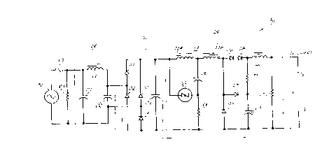
Fig. 1 illustrates a schematic of a ballast circuit
for operating a gas discharge lamp 12. The gas
5 discharge lamp 12 may be of the high efficient metal
halide type described in U.S. Patent 4,161,672 of D. M.
Cap and Lake issued July 17, 1979 or any DC operating
lamp which exhibits a gaseous discharge. The ballast
circuit 10 comprises an input filter stage 14, a AC to
10 DC converter 16, and a starting circuit 18. The
ballast circuit 10 may receive its excitation from a
typical AC power source 20 having a voltage of about
120 volts AC and a frequency of 60Hz. Other power
sources 20 may find application to the present
invention such as those found in Japan and European
countries.
The ballast circuit 10 comprises a plurality of the
conventional elements of the type indicated or having
typical components value both as given in Table 1.
TABLE 1
Element Value or Type
C1 1.5
C2 4.0
C3 1.2
C~ 0,15
C5 0.022
L1 0.95 henries
L2 100 microhenries
R3 1M
R4 12K
R5 1
R6 10K
R7 lOM
S1 sidac
D1-D4 IN4007
D5 and D7 Sanken RC2 (fast
recovery 2KV)
D6 and D8 GP10N (fast
recovery 1.1KV)
-~0 T1 Tapped inductor
.'C !7 ~l ~
r V° 4I~d
-6- LD 10,055
*Notes - Resistors are given in ohms
- Capacitors are given in microfarads
The ballast circuit 10 operates the discharge lamp
12 by the application of various levels of DC excitation
during its start, glow and run modes. The type and
values of the circuit components of the present
invention given in Table 1 of the ballast circuit 10 are
selected so as to automatically and sequentially provide
desired transfer functions of the circuit 10 that are
determined and interrelated to the impedance values of
the lamp occurring during its start, glow and run
modes. The ballast circuit 10 automatically provides
these functions for the lamp as it transitions into or
reverts from its start, glow and run modes of
aperation.
The ballast circuit 10 related to the present
invention provides DC excitation to the lamp 12 which
includes the necessary voltages and current conditions
so as to transition the gas discharge lamp 12 from its
(1) initial state requiring a high applied voltage of
about a 1KV to cause an initial break down of the gas
discharge lamp, which causes the lamp to (2) enter its
positive resistance region commonly referred to as its
glow mode that requires a compliance or glow voltage of
about 300 volts, and then transitions the lamp to (3)
its final arc or run mode. The high voltage 1KV is
applied and then reapplied until the lamp obtains its
start condition. As will be discussed, the starting
signal developed by the starting circuit of the present
invention improves or aids in the starting of the
discharge lamp relative to prior methods. Once the
break down or start mode is completed, the lamp goes
into and completes its glow mode, and then it sequences
into its run mode.
Once the lamp reaches its run mode, the DC voltage
~~1~~ gird
- LD 10,055
applied to the lamp changes Pram the compliance or glow
voltage of about 300 volts to about 30 volts and then
slowly rises to about 90 volts during the run mode.
Once the arc condition during the run mode of the lamp
has been established and the temperature has reached its
steady state value, the lamp has obtained its run or
steady state condition and the ballast circuit 10 allows
for the maintenance of such.
The input filter stage 14 of ballast 10 of Fig. 1 is
arranged across the power source 20 in a ~r type and
comprises capacitors C1 and C2 and an inductor L1. As
will be explained in more detail hereinafter with
reference to Fig. 6, one of the capacitors C1 has an
impedance value selected so as to cause the ballast
circuit l0 to present a relatively high power factor. to
the AC source 20 during the run mode of the lamp 12.
The components L1 and C2 farm an LC circuit whose
undampened resonant frequency is about 80Hz. This LC
circuit amplifies the 120 volts 60 cycle signal from the
power source 20 to approximately 300 volts which is
applied to the AC to DC converter 16. The AC to DC
converter 16 is comprised of diodes D1 through D4
arranged as a full wave rectifier which provides DC
output voltage that is preferably filtered by capacitor
C3.
The DC voltage at the output stage of the AC to DC
converter 16 is dependent or determined by the impedance
value RT of the gas discharge lamp which sequences in a
downward manner during the start, glow and run modes and
may be further discussed with reference to Fig. 2.
Fig. 2 shows the components of Fig. 1 that are
effective as to a first order approximatian, that is
with 10$, of the circuit during the run mode. Fig. 2
represents an intermediate illustration in the
establishment of the equivalent circuit related to the
run mode. By first assuming a lamp resistance of RT,
~~, w'~%'~.
-g- LD 10,055
one can transform the lamp impedance to the bridge
converter by realising that the current flowing to the
lamp, and therefore the current flowing in inductor
T1, is continuous. T1 is shown as comprising two
windings Tl_A and T1B which act as two mutually
coupled inductors. As shown in Fig. 2, the transformer
T1 merely operates as an inductor to filter the AC
component of the rectified current. Based upon this
assumption of RT and this filtering condition of T1,
the equivalent circuit of the run circuit may be as
shown in Fig. 3.
Fig. 3 is similar to Fig. 2 in that it illustrates
the input stage 14 but is different thereto in that it
shows L1 as comprised of a series resistance R1 and
an inductance L. Fig. 3 represents the equivalent
circuit related to the run mode and also illustrates
expressions (1) and (2) related to the transfer function
of circuit 10, to be described, associated with the run
mode of operation. Fig. 3 illustrates the equivalent
circuit in a two-port network manner. The input voltage
to the network is termed V1 and corresponds to power
source 20, and the output voltage to the network is
termed V2. V2 is an AC voltage corresponding to the
reflected lamp voltage capable of being measured across
C2. The current flowing through L1 and R1 is
termed I. The current I, shown in Fig. 3, may be
represented by expression (1) as:
I ° I1 - IC1 (1)
where I1 is the current flowing from the source
V1 and
IC1 is the current flowing through capacitor C1.
The current I may be further represented by
expression (2) as:
-9- LD 10,055
z (J w ) - I1 (J w ) - J (V1 w C1) (2)
where w is the frequency of V1 and
- 2~r ~ 60 = 377 radians/second.
The resistance across the V2 is termed R2 which
is substantially greater than the series resistance
R1 and has a value represented by expression (3)
shown on Fig. 3.
The condition of the currents and voltages shown in
the equivalent circuit of Fig. 3 is expressed by the
transfer function G1 shown in expression (4) of Fig.
3. The transfer function G1 of expression (4) is
represented in terms of (1) damping factor e, (4) the
frequency ( w) of V1 in radians/second, (3) the
natural frequency (w n) of the filter 14 in
radians/second and in terms of the (4) resistor,
capacitor and inductor components shown Fig. 3. The
transfer function of expression (4) illustrates that
the circuit composed of L1 and C2 responds to any
and all load demands, as mandated by the Lamp
characteristics, to establish the proper voltage and
current for the lamp during the three modes of
operation, start, glow and run. The transfer function
of expression (4) is plotted in Fig. 4 with the damping
factor being the implicit variable.
Fig. 4 has an X coordinate represented of the
quantity w / w n from 0.1 to 8.0 shown by the logl0
grids. Fig. 4 has two Y coordinates with the first one
representing a dependent variable Lm meaning "log
magnitude" and expressed as Lm = 20 LOG G1 (~ w).
The first quantity Lm is measured in decibels (db).
The second Y coordinate represents the phase angle
between the source 20 and the reflected lamp voltage as
discussed with regard to R2 of Fig. 3 and is given in
degrees. The quantity Lm is shown as having a range
of -30 db to l5db, whereas, the phase angle is shown as
~~~~~,~i~~
-10- LD 10,055
having a 0 degree (in-phase) to -180 degree range.
Fig. 4 shows a plot of a family of characteristic
curves having damping factors with values shown as
being grouped under under 22A of 0.10, 0.15, 0.20,
0.25, 0.30, 0.50, 0.71, and 1.00. These values 22A
are interrelated to (1) an upper plot of curve portions
22~, (2) a central plot of curve portions 22o and
(3) a lower plot of curve portions 22D. The upper
plots 22B and the lower plots 22D are continuous
and focus or merge at the intersection of Lm of about
-7.5 db, a phase angle of 90°, and a quantity w/ Wn
of 1Ø The 12 db/octave break-point related to the
lower merger point of the quantities of 22~ is shown
in F'ig. 4 by reference number 24.
The load trajectory 26 associated with the various
operational modes of circuit 10 is superimposed on the
family of the characteristic curves primarily related
to plot 22~ as shown in Fig. 4. The desired
operating point for the glow mode is shown on the load
trajectory by reference number 28, whereas, the desired
operating point for the run mode is shown by reference
number 30. Operating point 30 lies directly on the
plot 22~ related to damping factor 0.71 curve,
whereas, operating point 28 lies directly on the plot
22 related to damping factor 0.10. Over a period of
time, as the lamp 12 ages, the steady-state operating
point 30 moves (travel) on the vertical load trajectory
line 26. For example, the operating point moves from a
damping factor curve 0.71 upward toward a damping
factor curve of 0.5. Further, as the power source 20
represented in Fig. 3 as V1 changes, the operating
point 30 similarly move either above or below the
operating point 30 of that shown in Fig. 4. It is
desired that the operating point 30 of the run mode not
fall below the 0.5 damping factor value.
The operation of the ballast circuit 10 during the
t ~~."~n:a~ r~
~u~~li~
-11- LD 10,055
run mode of the gas discharge lamp 12 may be further
described with reference to Fig. 5 showing expression
(5) and (6) both related to transfer function G2
representative of the input of the circuit of Fig. 3 as
it may appear to the applied voltage V1. The
transfer function G2 illustrates that when the nin
circuit is loaded by the lamp, the circuit reacts in
such a way as to establish a current whose phase angle
with respect to the power line voltage is easily
corrected by a single reactive component C1 in a
manner to be described. The terms in expressions (5)
and (6) are the same as those described with regard to
expressions (3) and (4) except for the addition of Za
which is the characteristic impedance of the filter 14
expressed in terms of L1 and C2. It should be
noted that C1 is lacking in any of the terms of
expressions (3) and (4). The void of C1 is intended
so as to describe the background for the effect of C1
in the easily obtainable desired power factor.
Assuming the values of the quantities for ~, Zo,
~ n and V1 shown as being related to expression
(5), and then substituting these values and quantities
into expression (5) yields the values shown in
expression (6) for I (e). Further assuming a damping
factor of 0.71 for the run mode, then using those
quantities of expression (6) yields a phase angle of
45°. Assuming this 45° phase angle during the run
mode, then it becomes known that the current lags the
applied voltage across lamp 12 by 45°, which then
yields a power factor that is undesired for the
operation of a gas discharge lamp especially when such
operation desires constant power to be applied and
maintained across the lamp 12. The phase angle of the
input current to the ballast circuit having the
equivalent circuit of Fig. 3 as a function of damping
factor and without the benefits of C1 of Fig. 3 is
~ il ~ i ~ a ~_
-12- LD 10,055
shown in Fig. 6.
Fig. 6 has a Y coordinate showing the phase angle
a (e) between I and V1 having a peak of about a
positive +90° and a valley of about a -90°. Fig. 6
also has a X coordinate representative of the damping
factor a and showing the previously discussed, with
regard to Fig. 4, damping factor quantity 0.71 related
to the run mode of ballast 10. Fig. 6 shows the
intersection of the damping factor of 0.71 as
corresponding to an angle of -45°. This phase angle of
-45 is corrected by the present invention by providing
a nearly unity power factor caused by the selection of
the value of capacitor C1. For example, for the
description previously given above with regard to the
input filter 14 having C1, the value of C1 may be
selected in the range of 1.5 to 3.0 microfarads. One
of the advantages of the input filter 14 having the
capacitor C1 is that a desired power factor is easily
obtained by the selection of the value of a single
capacitive component C1. This easy selectable
capacitive method to provide the power factor
correction is due in part to the nearly sinusoidal
nature of I occurring during the run mode of
operation. This method provides a power factor of not
less than 0.90.
The values of C1 from 1.5 to 3.0 microfarad are
related to a typical 60 Hz power. These desired values
change as the frequency of the power sources changes
such as to those found in Europe and Japan. Further,
if desired, the 3.0 microfarad value may be exceeded so
that the phase angle a (e) may become a positive (+) or
leading quantity. The ability to select a single
component to provide for the desired phase angle a (e)
is an important feature of the present invention. The
practice of the present invention allows for the
designer to first establish the desired amplification
C y 'r ;1 s'e a
~i~G~U~:~
-13- LD 10,055
needed for the compliance voltage obtained by the
selection of the values of L1 and C2. Then the
designer may determine the desired transfer functions
for the desired run operation of the lamp. Finally the
designer may then select a particular value for C1 to
provide for the desired power factor.
Prior to the attainment of the run mode of
operation, the lamp 12 passes through the glow mode.
In the glow mode, the lamp 12 requires about 300 volts
DC for its compliance or glow voltage and about 10
milliamps of current in order for the lamp to establish
an arc condition to allow it to pass into the run
mode. During the glow mode, the ballast 10 accepts the
power line voltage which can vary from 108 to 132 volts
and amplifies such by the operation of the resonant
network L1 and C2. Network 16 of Fig. 1 then
rectifies the output of L1-C2 to about 300 volts
DC.
Referring to Fig. 4 and moving upward along the
load trajectory 26 from operating point 30 toward
operating point 28, it is seen that as the damping
factor diminishes in value, the output voltage V2
increases indicated by an increased peaking in the
central plots 28C. A typical value of the Lamp
resistance is about 3oK during the glow mode, and the
resistance R2, previously discussed with regard to
Fig. 3, is therefore 30K. Substituting this value of
30K for R2 into expressions (5) and (6) of Fig. 5
along with the otter quantities given thereon, yield a
value of a damping factor a equal to 8.33.10 3.
This damping factor of 0.00833 is added to by the
residue values components (e.g., C4 and R5) of the
start circuit, to be discussed, and results in an
equivalent damping factor of approximately 0.1. As
seen in Fig. 4, this damping factor of 0.1 provides
sufficient amplification of 7db (about 2.4) so as to
~~ ~3 ;~ .~~ s:~ .-~
N~~~)E~:r_
-14- LD 10,055
transition the lamp into the nin mode.
A primary feature of the present invention is that
the needed circuitry for the individual modes of lamp
operation is segmented and automatically and
sequentially provides the desired circuit transfer
functions. The glow circuit which is primarily
comprised of the elements shown in Fig. 2 (including
C3 (not shown) of AC to DC converter 16) is
automatically activated if the arc condition occurring
during the run mode of the lamp extinguishes for any
reason. Similarly, the start circuit is automatically
activated whenever the lamp current extinguishes in
either the run or glow modes because the sidac S1 of
Fig. 1 and 7 is rendered conductive whenever the
voltage output of the AC to DC converter is greater
than 240 volts which corresponds to the breakdown
characteristic of S1. The start circuit that employs
the sidac S1 may be further described with reference
to Fig. 7.
A primary feature of the starting circuit 18 of
Fig. 7 is to develop a relatively high DC voltage level
(about 1200V DC) upon which occurs pulses (about
300V DC) having a repetition rate of about 2.5m sec.
In general, this signal is developed by an oscillator
circuit whose voltage output is amplified by T1,
rectified by D6 and D8 and filtered by C5 as a
means to produce a nearly DC voltage of sufficient
amplitude to cause the lamp to conduct. The developed
signal provides for better starting of the discharge
lamp relative to prior art methods.
The sidac S1 of the start circuit 18 is selected
to have breakdown voltage characteristic such that it
is; (1) rendered conductive when the DC voltage, for
example 300 volts, at the output stage of the converter
16 corresponds the impedance value, such as 500K ohms,
of the gas discharge lamp occurring during its starting
-15- LD 10,055
mode; and (2) is maintained in its non-conductive state
when the DC voltages of less than 240 volts and less
than about 90 volts correspond to the impedance value
of the gas discharge lamp such as 250f1 and 30K
occurring during the run and glow modes respectively.
When the output of the AC to DC converter 16
exceeds about 240V DC (typically at about 300V DC), it
excites a 400Hz relaxation oscillator comprised of
R4, C4, S1 and T1A in which the values of R4
and C4 primarily determine the frequency of
oscillation. The 300V DC level causes sidac S1 to be
rendered conductive, which, in turn causes capacitor
C4 serving as a first energy storage means and having
a stored value of about 240V to discharge into T1
having a mutually coupled winding to establish a high
voltage. The operation of T1 having the windings
T1A and T1B develops a voltage of about 960V which
is additive with 240V of C4 and the 300V of the
converter 16 so as to generate a voltage of about 1500V
across T1 which is shown as a pulsed waveform 32
across T1B. This 1500V signal is rectified by diodes
D6 and D8 along with diode D7 which directs the
1500V DC signal to charge a second energy storage
device capacitor C5. This signal also appears at the
input to L2, via resistor R6 which prevents rapid
discharging of C5, and is shown as signal 34.
Signal 34 is shown as a pulse waveform having a
peak amplitude of about 1500V DC which decays to a
value of about 12o0V DC. The time constant decay of
signal 34 is about lOm sec. and is determined by the
value selected for C5 (0.22 microfarads) and the
impedance value (about 500k) of lamp 12. The signal 34
has a repetition rate of about 2.5m seconds. The
characteristics of signal 34, in particular the high DC
level having the pulses extending therefrom, provides
for easier starting of the discharge lamp relative to
~~~~i;~%~.~.
-16- LD 10,055
prior methods.
The starting circuit 18 preferably further includes
an inductor L2 connected to the arrangement of diodes
D8 and D6. The inductor has a value selected,
previously given, to limit the amplitude and the rate
of change of the current applied to the lamp during the
entrance to the glow mode from the start mode. The two
diodes D8 and D6 shown in dig. 7 may be replaced
with a single high voltage type diode.
The resistor R6 in addition to providing a path
for the development of signal 34 also reduces the
susceptibility of the lamp to °'back arcing'° by
increasing the impedance path from the lamp 12 to the
capacitor C5. By °'back arcing'° it is meant that an
arc strikes off the back of one of the electrodes of
the lamp typically caused by high di/dt conditions
experienced by lamp 12. The diode D~ facilitates the
charging of C5, which reduces the high voltage ripple
to which lamp 12 is subjected. The charging time of
CS is related to C5 and the series resistance of
T1B.
Still further, it is preferred that a diode D5 be
included in the starting circuit and arranged so as to
be reversed biased when the switching means S1 is in
its non-conductive state. In this arrangement D5
performs a clamping function in that the output of
T1B (side attached to D5, D6 and D~) will go
negative (voltage) each time the current through sidac
S1 is abruptly stopped. The diode D5 clamps this
negative voltage and prevents D6 and D8 from being
damaged due to excessive reverse voltage.
The inductor T1 of the starting circuit 18 is
preferably a tapped inductor and is used instead of a
transformer so as to provide a step-up function for the
development of signal 34. The usage of the tapped
inductor improves the manufacturability of the power
:,~~~;,,:j.~ 7
:..z GJ ~J it
LD 10,055
circuit and decreases the cost while at the same time
improving the efficiency of the high voltage circuit.
Further improvement for the ballast circuit 10 is
shown in Fig. 1 with reference to the resistors R5
and R3. The resistor R5 is of a low value and in
actuality is a fuse serving as a protection function.
The resistor R3 provides a bleeder function to
provide a path for the discharging of C1 and C2.
It should now be appreciated that the practice of
the present invention provides for the ballast circuit
having the desired transfer functions that
automatically sequence as the lamp transitions from its
(1) start to its (2) glow, and then to its (3) run
modes of operation. The desired transfer impedance is
automatically obtained during any of the operating
modes of the metal halide lamp.
Further, it should be appreciated that the
practices of the present invention limits the amplitude
and rate-of-change of current surges typically
experienced when the lamps related to the present
invention enter into the glow mode from the start
mode.
Still further it should be appreciated that the
practice of the present invention allows for a easily
adaptable selection of a single reactive element C1
that provides for a high power factor not less than 0.9
for the ballast circuit 10.