Note: Descriptions are shown in the official language in which they were submitted.
2038223
RCA 85,964
TELEVISION RECEIVER WITH AUXILIARY INPUT
CONNECTOR FOR VIDEO SIGNALS OF A
SEPARATED Y-C FORMAT
This invention relates to television receivers and
particularly to receivers intended for use with auxiliary video input
signals of a non-composite type having separate luminance and
chrominance components.
Video cassette recorders (VCR's) and combination camera-
recorders (cam-corders) have been proposed that provide a relatively
wideband luminance signal response (e.g., 5 MHz) and which include an
output connector (commonly called an "S-terminal") that provides
separated luminance and chrominance output signals. This new video
interconnection standard is commonly known as the "SVHS" video
1 5 format which stands for "super VHS". An advantage of this new (non-
composite) video inter-connection format is that one may apply the
separated luminance and chrominance signal to the display processing
circuits of a television receiver directly without going through the
receiver's internal luminance-chrominance signal separation filter (e.g.,
2 0 a comb filter). Advantageously, the SVHS video signal format
eliminates interference effects such as cross-color and cross-luminance
which otherwise could occur if the luminance and chrominance signals
were to be combined as a composite video signal for application to the
receiver.
2 5 Television receivers suitable for processing and displaying
video signals of either composite form or of a separated luminance-
chrominance signal format are known. An example is shown and
described in UK Patent Application GB 2, 134, 743 A of Tanaka
published 15 August 1984 and entitled COLOR DISPLAY SYSTEM. In
3 0 this system video input signals of composite type are applied to a comb
filter for separation into comb-filtered luminance and chrominance
components which are applied by means of respective switches to
corresponding luminance and chrominance input of a display processing
unit. The system includes a pair of input terminals for receiving
3 5 respective ones of the luminance and chrominance components of a
non-composite video input signal. For displaying signals of this format
the switches are changed over to disconnect the comb filter from the
display processor and connect the input terminals of the non-composite
1
2038223
RCA 85,964
signal source to respective ones of the luminance and chrominance
input terminals of the display processor.
Another example of a color television receiver having
provisions for displaying signal of both composite and non-composite
format is the "RCA" brand receiver employing the chassis type number
CTC-159 manufactured and sold by Thomson Consumer Electronics, Inc.,
of Indianapolis, Indiana. In this receiver the comb filter includes
emitter follower output stages for applying the comb filtered
luminance and chrominance signal to the display processor. The
luminance and chrominance components of the non-composite (S-VHS)
input signal are applied to respective output of the comb filter by
means of respective switched amplifiers. The amplifiers are switched
OFF to enable display of a composite video signal applied to the input of
the comb filter. To display the S-VHS signal the amplifiers are switched
ON thereby reverse biasing the emitter follower output transistors of
the comb filter and coupling the amplified luminance and chrominance
component of the S-VHS input signal to respective inputs of the display
processor. Advantageously, this technique of selecting signals for
display provides amplification as well as switching as compared with
2 0 the system of Tanaka described above which only provides switching of
the composite and non-composite signals. A further feature of this
receiver is that a mufti-pole input switch is provided for selecting one
of a plurality of composite video input signals for application to the
input of the comb filter and this switch is coupled to the comb filter by
2 5 means of an amplifier whereby each composite video signal that is
selected for display is subjected to amplification by the amplifier
preceding g the comb filter and the S-VHS luminance and chrominance
components are separately amplified by respective ones of the two
switched amplifiers connected to the comb filter output terminals.
3 0 A color television receiver embodying the invention includes
a comb filter having luminance and chrominance outputs coupled to
respective inputs of a display processor and having a signal source for
providing a composite video input signal having combined luminance
and chrominance components and providing a non-composite video
3 ~ input signal having separated luminance and chrominance components.
Circuit means are provided having a first operating mode for coupling
the composite video signal to an input of said comb filter for enabling
display of said composite video input signal by said display processor
2
2038223
RCA 85,964
and having a second operating mode for coupling said luminance
component of said non-composite video input signal to said input of said
comb filter and for concurrently coupling said chrominance component
of said non-composite video in put signal to said chrominance output of
said comb filter for displaying said non-composite video input signal by
said display means.
The invention is illustrated in the accompanying drawing
wherein like elements are denoted by like reference designators and in
which:
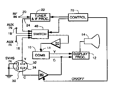
1 0 FIGURE 1 is a block diagram of a color television receiver
embodying the invention;
FIGURE 2 is a circuit diagram, partially in block form, of an
input video selection switch suitable for use in the receiver of FIGURE 1;
and
1 S FIGURE 3 is a circuit diagram of a switched amplifier
suitable for use in the receiver of FIGURE 1.
The color television receiver of FIGURE 1 includes a comb
filter 10 having luminance (Y) and chrominance (C) outputs coupled to
respective inputs of a display processor 12 having an output coupled to
2 0 a display device {e.g., a kinescope) 14 for displaying signals applied to
the display processor 12. The receiver includes a signal source for
providing a composite video input signal having combined luminance
and chrominance components and for providing a non-composite video
input signal having separated luminance and chrominance components.
2 5 The signal source comprises auxiliary input terminals 16 and 18 for
receiving baseband composite video irput signals from a VCR or other
suitable source and a tuner 22 having an antenna input 20 for receiving
an RF modulated television signal and an output 24 providing a
baseband composite video signal. The signal source also includes an S-
3 0 VHS connector 30 for providing a non-composite video input signal of a
format having separated luminance and chrominance components
provided at respective terminals 32 and 34 of S-VHS connector 30.
The color television .receiver of FIGURE 1 further includes
circuit means for facilitating the display of input signals of composite
3 5 and non-composite format. The circuit means includes an input switch
40 having inputs connected to apply the baseband composite video
output signal of tuner 22, the auxiliary baseband composite video
signals provided by terminals 16 and 18 and the luminance component
3
2038223
RCA 85,964
of the S-VHS signal provided by terminal 32 to the input 11 of comb
filter 10 via a switched amplifier 50. The circuit means also includes a
switched amplifier 60 for coupling the chrominance component of the S-
VHS video signal (non-composite) provided at terminal 34 to the
chrominance output (C) of comb filter 10. A control unit 70 supplies
control signals to tuner 22 for controlling channel selection, to switch 40
for controlling selection of input signals to the comb filter 10 and to the
switched amplifier 60 for controlling coupling of the chrominance
component of the S-VHS signal to the output of comb filter 10.
In operation, when standard broadcast or cable TV channel
signals are to be displayed, control unit 70 sends a disabling signal to
switched amplifier 60, a channel selection signal to tuner 22 and a
control signal to switch 40 for conditioning the switch 40 to apply a
selected composite video input signal to terminal 11 of comb filter 10
corresponding to the broadcast or cable channel received. Comb filter
10 separates the luminance and chrominance components of the tuner
selected composite video signal and applies them to the inputs of
processor 12 for display by display unit. The same operation takes
place when selecting either of the auxiliary composite video input
2 0 signals AUX-1 or AUX-2.
When the non-composite video input signal provided by S-
VHS input connector 30 is to be displayed the processing changes.
Specifically, control unit 70 sends a control signal to video input switch
40 for causing switch 40 to apply the luminance component of the S-
2 S VHS signal to the input 11 of comb filter 10 via amplifier 50.
Concurrently, control unit 70 enables switched amplifier 60 to coupled
the chrominance component of the S-VHS signal (at terminal 34) to the
chrominance output of comb filter 10. The comb filter 10 is preferably
of a type having an emitter follower output stage and when the
3 0 chrominance signal is applied thereto be switched amplifier 60 the
output transistor of the emitter follower is thereby reverse biased.
Although it is preferred that comb filter have an emitter follower
output, this is not essential to the invention because the signal applied
to the comb filter in this mode does not contain a chrominance
3 5 component and therefore it is not possible for the the chrominance
output of the comb filter to interfere with the chrominance signal
coupled from terminal 34 of the S-VHS connector. However, when
conventional composite video signals are being displayed the switched
4
2038223
RCA 85,964
amplifier 60 ensures that the S-VHS chrominance signal (if present)
does not interfere with the chrominance component of the composite
video signal being processed.
The color television receiver of FIGURE 1 has a number of
advantageous features over the prior art receivers previously discussed.
Firstly, it will be noted that even though the luminance component of
the non-composite video signal is subjected to comb filtering, it never
the less is never mixed with the S-VHS chroma signal and so there is no
possibility of undesirable cross-color or cross- luma effects. Moreover,
it will be noted that all signals are subjected to amplification by only
two amplifiers (50 and 60) whereas for the known receiver three
amplifiers were required. This reduction in the number of amplifiers
required desirably improves the overall reliability of the color
television receiver due to the reduction of parts needed to implement it
and provides an obvious economic benefit as well.
FIGURE 2 is exemplary of a presently preferred embodiment
of the switch 40 of FIGURE 1. Other switches, suited for operation at
video frequencies may be used instead. The preferred switch is
described in detail in US patent application Serial No. 441901 filed
2 0 November 28, 1989 by the present inventor. The switch comprises a
type CD 4052 B CMOS integrated circuit 200 which has a four position
switch (A-D) and a decoder 202 for controlling the switch. The switch
output is connected to a load resistor 204 to which amplifier 50 is
connected and the four switch inputs of the integrated circuit 200 are
2 5 ' coupled to terminals 20, 16, 18 and 32 via respective coupling networks
210-214. Each network includes an input terminating resistor 220-223
a Zener diode 230-234 coupled between the CMOS switch input and
ground, a series connected resistor (240-243) and capacitor (250-253)
coupled between the video input terminals and respective CMOS switch
3 0 input terminals and a bias resistor ( 260-263) coupled between a
supply voltage terminal 270 and respective cathodes of the Zener
diodes 230-233.
In operation, decoder 202 decodes control signals provided
by control unit 70 to close one of four of the switches A-D of CMOS
3 5 switch 200 to thereby select one of the input signals at terminals 20, 18,
16 and 32 for application to load resistor 204 and amplifier 50. As an
example, if the tuner input 20 is not selected then switch A will be open
and Zener diode 230 will be forward biased by current flow from
5
2038223
RCA 85,964
resistor 260. This condition provides attenuation of the signal at
terminal 20 by both the open switch A and by the "L" type attenuator
formed by resistor 240 and forward biased Zener diode 230;.
Conversely, when switch A is closed the bias current for Zener diode
230 is diverted to ground by means of the load resistor 204.
Accordingly Zener diode 230 turns off and provides no attenuation and
the switch section A couples the input signal at terminal 20 to the
amplifier S0. The same operation occurs for the remaining switch
sections. Other advantages of this switching arrangement are described
in US patent application Serial No. 441,901 filed November 28, 1989 by
the present inventor.
FIGURE 3 is an example of a presently preferred switched
amplifier which may be used in the example of FIGURE 1. Other
switched amplifiers may be used instead. In FIGURE 3 the S-VHS
chrominance input terminal 34 is coupled to ground by an input
terminating resistor 300 and is coupled to a circuit node 306 via an
electro-static discharge (ESD) protection resistor 302 in series with a DC
blocking capacitor 304. Node 306 is coupled to ground via series
connected resistors 308 and 310 and a switch 312 controlled by control
2 0 unit 70. The common connection of resistors 308 and 310 is coupled to
ground via a bypass capacitor 314 thereby forming a low pass filter
which isolates noise with may be present in switch 312 from node 306
and also isolates chrominance present at node 306 from other signals
which may be switched by additional switch sections in switch 312.
2 5 Node 306 is further coupled via the cathode-anode path of a diode and
a resistor 322 to the base of a NPN transistor having an emitter coupled
to ground via an emitter resistor and having a collector coupled to a
supply terminal 330 via a collector load resistor 328. The supply
terminal is also coupled to the anode of Zener diode 320 via a bias
3 0 resistor 332. The collector of transistor 324 is coupled to the base of an
output transistor 340 having a collector connected to supply terminal
330 and an emitter connected to the output of comb filter 10. The
emitter follower output stage of comb filter 10 is outlined in phantom
and includes an NPN transistor 350 having an emitter coupled via a
3 5 current source 360 to ground.
In operation when control unit 70 closes switch 312 a
current will flow through resistors 332, 308 and 310 and diode 320 to
ground thereby simultaneously forward biasing diode 320 and biasing
6
2038223
RCA 85,964
amplifier transistor 423 for linear operation. The input signal at
terminal 34 is conducted by diode 320 to amplifier transistor 324,
amplified and applied by emitter follower 340 to the output terminal
with transistor 340 being biased at a sufficiently positive voltage (e.g., 9
S volts) to reverse bias the emitter follower 350 transistor of comb filter
which is biased at a lesser voltage (e.g., 6 volts). When control unit
70 opens switch 312 there is no DC path for the cathode of diode 320.
Accordingly, for this condition current provided by resistor 332
saturates transistor 324 and drives the emitter follower transistor to a
10 low potential thereby reverse biasing the base-emitter junction of
transistor 340 and enabling the emitter follower 350 of the comb filter
10 to coupled comb filtered output signals to the processor 12. At the
same time diode 320 rectifies the input signal at terminal 34 and thus
generates a self-bias voltage which reverse biases diode 320 and
thereby provides additional attenuation of the signal at terminal 34 in
addition to the attenuation provided by the reverse biased emitter
follower transistor 340.
7