Note: Descriptions are shown in the official language in which they were submitted.
2 ~ ~ -J '.~
An ATM Cell Broadcasting System
Background of the Invention
Field of the Invention
This invention pertains to a digital switching
system, and more particularly to an ATM (Asynchronous
Transfer Mode) cell broadcasting system utilized in
ATM switches, e.g. for ISDN (Integrated Service
Digital Network), which exchange ATM cells
representing information having different traffic
characteristics such as voices, data and moving
images.
Description of the Related Art
With the recent widespread use of data
communication, publicly switched networks now carry
important data, as well as traditional voices, and are
required to offer high-quality data transmission and
exchange.
As a communication network for serving not only
low speed data such as voice data, but also high speed
data such as moving images, a broadband ISDN (B-ISDN)
has begun to be put into practical use and various
interfaces are being standardized. Unlike
traditional switching methods, a B-ISDN utilizing an
asynchronous transfer mode (ATM) can commonly carry
2~8~
various sorts of information at different speeds, e.g.
voice data, moving image data and even continuous
information mixed with burst information.
An ATM communication network transmits and
exchanges information of different bands divided and
housed in fixed-length data units called cells,
instead of information divided and housed in variable-
length packets used in traditional packet
communication. Cells containing channel data are
indiscriminately multiplexed, transmitted over optical
fibers at high speed, and fast-exchanged by hardware
switches. Thus, an ATM communication network can
offer flexible services requiring different
transmission speeds and makes efficient use of
transmission paths.
User information is divided into several pieces
according to its length and cells are configured by
adding headers, e.g. of a few bytes, to the respective
data, e.g. of 32 to 120 bytes, comprising the divided
pieces of information. A header contains a virtual
channel identifier (VCI) for identifying the
originating user of the corresponding data. Thus,
user information stored in cells is multiplexed over
ATM highways before it is transmitted and exchanged.
Switch elements in a switch matrix route cells to
r ~
their respectively connected output highways, when
they are turned on.
That is, a conventional switch matrix enables
one-to-one communication by outputting an ATM cell
inputted from an input highway to only one of a
plurality of output highways. Therefore, there is a
problem that it lacks the capacity for one-to-many
communication, i.e. from one originator to a plurality
of destinees, by outputting an ATM cell inputted from
an input highway to a plurality of output highways.
Summary of the Invention
An object of the present invention is to bordcast
data stored in cells to a plurality of destinees by
outputting the cells to a plurality of output highways
in an ATM switch.
An ATM (Asynchronous Transfer Mode) cell
broadcasting system is utilized in ATM switches, e.g.
for ISDN (Integrated Service Digital Network), which
exchange ATM cells representing information having
different traffic characteristics such as voices, data
and moving images.
It configures a switch matrix, for exchanging ATM
cells inputted from an input highway by outputting
them to a plurality of output highways, to be provided
with tag information adders, for adding to the ATM
~ 2~3~6~
cells tag information corresponding to the VCI of the ATM
cells, at its respectlve input terminals connected to input
hlghways.
According to a broad aspect of the invention there
is provlded an asynchronous transfer mode cell broadcastlng
system comprislng a swltch module includlng a plurallty of
switches for exchanglng asynchronous transfer mode cells
lnputted from an lnput line connected to N swltches of sald
plurality of swltches; and a tag lnformatlon adder, provlded
ln the lnput line, for adding tag lnformatlon lncluding N
bits, each blt belng respectlvely allocated to a correspondlng
one of said N switches, sald tag informatlon lndlcating
whether each of said N switches outputs a cell from the lnput
llne accordlng to a respective ldentifier asslgned to an
asynchronous transfer mode cell so that sald asynchronous
transfer mode cells are outputted to a plurallty of output
llnes connected to the switches deslgnated by the tag
information.
According to another broad aspect of the lnvention
there ls provlded an asynchronous transfer mode cell
broadcasting system comprising a swltch module lncluding a
plurality of swltches for exchanglng asynchronous transfer
mode cells inputted from an input line; and asynchronous
transfer mode-cell-swltchlng ldentifler determinant memorlzing
means, each provided for a respective switch in said switch
module, sald memorizing means storlng, accordlng to respective
ldentifiers assigned to said asynchronous transfer mode cells,
28151-36
t~
- . ~
r ~ 5 6 ~
determlnant data information for indicating which ones of sald
asynchronous transfer mode cells are to be switched and whlch
ones of said switches are to be turned ON so that the
asynchronous transfer mode cells which are switched based on
said determinant data information are outputted to a plurality
of output lines connected to the switches which are turned ON
according to said determinant data informatlon so as to enable
said asynchronous transfer cells to be broadcast to a
plurality of destinations.
In accordance with the present invention there is
provided a switching information adding apparatus for a
switching system accommodating a plurality of input lines and
a plurality of output lines, said plurality of input lines
being connected to said plurality of output lines through
gates, said switching information adding apparatus comprising
a receiver for receiving a flxed-length packet including
destination information transmitted over at least one of said
plurality of input llnes; a storage for storing switching
information indicating whether or not a fixed-length packet is
made to go through each of the gates connected to sald at
least one of said input lines corresponding to the destlnation
information of the fixed-length packet; an information adder
for addlng swltching information obtained from said storage
based on the destinatlon informatlon of the flxed-length
packet to the fixed-length packet; and an output unlt for
outputting the flxed-length packet having the switchlng
information to the switching system.
4a
28151-36
In accordance with the present inventlon there is
also provided a swltch for accommodatlng an lnput llne and a
plurality of output llnes, sald input llne belng connected to
said plurality of output llnes through respective gates, for
outputtlng a fixed-length packet having switching information
transmitted from said lnput line to sald plurality of output
lines on the basis of the switching lnformation, sald switch
comprising an information analyzer, provided for each of the
gates, for obtainlng information which is allocated to a
specific gate from the switchlng lnformation included ln the
fixed-length packet and for determining whether or not
corresponding information lndlcates that the flxed length
packet is to go through the speclfic gate; and a controller,
provlded for each of the gates for havlng sald fixed-length
packet go through the specific gate when the information
analyzer indicates that said flxed-length packet ls to go
through the speclflc gate.
In accordance with the present invention there is
further provided a flxed-length packet broadcastlng system
comprlslng a swltch module lncludlng a plurality of switches
for exchanging fixed-length packets inputted from an input
line connected to N swltches of said plurality of switches;
and a tag lnformatlon adderl provlded ln the input line, for
adding tag information including N blts, each bit being
respectively allocated to a corresponding one of said N
switchesl said tag information indicating whether each of said
N switches outputs a packet from the input line according to a
4b
28151-36
., ~
respective identifier assigned to a fixed-length packet so
that said fixed-length packets are outputted to a plurallty of
output lines connected to the switches of sald switch module,
designated by the tag informatlon.
In accordance with the present lnvention there is
provided a fixed-length packet broadcastlng system comprislng:
a switch module including a plurality of switches for
exchanglng flxed-length packets lnputted from an lnput llne;
and switching identifier determlnant memorizlng means,
provlded in said switch module, sald memorlzlng means storlng,
accordlng to respective ldentifiers assigned to said flxed-
length packets, determlnant data lnformatlon for lndlcatlng
whlch one of sald flxed-length packets are to be swltched and
whlch ones of sald swltches are to be turned ON so that the
fixed-length packets which are switched based on sald
determlnant data lnformatlon are outputted to a plurallty of
output lines connected to the swltches of sald swltch module,
whlch are turned ON according to sald determlnant data
informatlon so as to enable sald fixed-length packets to be
broadcast to a plurality of destinatlons.
Brief Description Of The Drawinqs
Figures lA and 1~ are block dlagrams respectively
lllustratlng a first and a second princlple of thls inventlon;
Flgure 2 shows an exemplary configuration of an ATM
cell;
Flgure 3 ls a block diagram showing the broadcastlng
system accordlng to the flrst prlnclple of thls lnventlon;
28151-36
~ 2~8~
Figure 4 shows exemplary contents stored in a tag
information memory;
Figure 5 is a flowchart of a switching ~udgment
embodylng the first prlnclple of this lnventlon;
Flgure 6 is a block diagram showing the broadcasting
system according to the second prlnclple of this lnvention;
Figure 7 shows exemplary contents stored in an ATM-
cell-swltchlng VCI/VPl determlnant memory for memorlzlng the
VCI/VPi of the ATM cells to be swltched; and
Flgure 8 ls a flowchart of a swltchlng ~udgement
embodylng the second prlnclple of thls invention.
4d
28151-36
. .i
2~$~6~
-- 5
Description of the Preferred Embodiment
The first and second principles of this invention
are explained by referring to Figures 1A and 1B, where
switch matrices 1A and 1B output, to a plurality of
output highways, ATM cells inputted from input
highways by exchanging them.
Figures 1A and 1B are block diagrams respectively
illustrating a first and a second principle of this
invention.
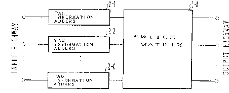
In Figure 1A, tag information adders 2-1 through
2-X are converters provided at respective N input
terminals connected to input highways in a preceding
stage of switch elements of switch matrix 1-A. They
add to the ATM cells tag information for
simultaneously outputting the ATM cells to a plurality
of output highways corresponding to the VCItVPi
(indicating the originator) of the ATM cells.
When switch matrix 1-A comprises e.g. 4*4 switch
elements [for four (4) input highways and four (4)
output highways], four (4) switch elements receive the
same ATM cells from an input highway. If the tag
information adder 3-i (where i is an integer from 1 to
4) corresponding to the input highway adds tag
information, e.g. 0101, to the ATM cells, the second
and fourth switch elements, e.g. from the input
2 ~ 3 ~ ?
-- 6
highway, are turned on and output the ATM cells to the
output highways connected to these switch elements.
In Figure 1B, ATM-cell-switching VCI determinant
memories 3-1 through 3-Y for memorizing the VCI of ATM
cells to be switched are provided at the M switch
elements in switch matrix 1-B. Upon receiving ATM
cells, the M switch elements judge whether or not they
should be turned on and output the ATM cells from the
corresponding input highways to the corresponding
output highways, by referring to the corresponding
ATM-cell-switching VCI/VPi determinant memories 3-1
through 3-Y. By variably setting routing
information utilizing VCI/VPis in ATM-cell-switching
VCI/VPi determinant memories 3-1 through 3-Y e.g. by
software, the switch elements, whose ATM-cell-
switching VCI/VPi determinant memories 3-1 through 3-Y
have the same VCI/VPis as the ATM cells inputted from
an input highway, output the ATM cells simultaneously
to a plurality of output highways.
Thus, this invention enables ATM cells copied in
a switch matrix to be transmitted simultaneously to a
plurality of destinees.
Figure 2 shows an exemplary configuration of an
ATM cell.
In Figure 2, an ATM cell has a total length of
2 ~ 3 ~ 3~
-- 7 --
fifty-four (54) bytes. Its two (2) head end bytes
store tag information for enabling the ATM cell
inputted from an input highway to be outputted
simultaneously to a plurality of output highways,
according to the first principle of this invention.
Next, after appropriate bytes for a virtual path
number and the virtual channel number corresponding to
a VCI, a maintenance datum of one (1) byte and message
data from an originator of the remaining bytes are
stored. According to the second principle of
this invention, no tag information is required. Thus,
the two (2) head end bytes remain empty.
Figure 3 is a block diagram showing the
broadcasting system according to the first principle
of this invention.
The switch matrix shown in Figure 3 comprises 4*4
switch elements for simplicity. In reality, a
plurality of such switch matrices configure a large
scale ATM switch. CNVs 10 through 40 are converters
for converting to tag information the VCIs of ATM
cells transmitted over corresponding input highways
and enabling the ATM cells to be outputted to a
plurality of output highways. On receipt of ATM
cells, CNVs 10 through 40 read the tag information
from a memory, not shown in the drawing, by using the
2 ~ 8
VCI/VPis of the ATM cells. The bit length of tag
information is equal to the number of switch elements
receiving the ATM cells from a same input highway.
In this case, since four (4) switch elements are
connected to the each input highway through a
converter, the tag information has four (4) bits.
As shown in Figure 2, the tag information is attached
to the ATM cells, which are inputted to switch
elements (SWs) 11-A through 44-A connected to CNVs 10
through 40.
Assume here that ATM cells are inputted via CNV
10 to SWs 11-A through 14-A, CNV 10 converts the VCI
of the ATM cells to 4-bit tag information 0101, and
respective bits of tag information from the highest
digit represent the flags of SWs 11-A through 14-A to
be turned on. Since SWs 12-A and 14-A are turned
on, they output the ATM cells to the output highways
connected to them. Since SW 11-A and 13-A are not
turned on, they do not output the ATM cells to the the
output highways connected to them. Thus, the ATM
cells of the same VCI inputted to CNV 10 are switched
to two (2) of the four (4) output highways, and the
ATM cells are broadcast to the intended destinees.
Figure 4 shows exemplary contents stored in a tag
information memory.
2 ~ 3 ~
CNVs 10 through 40 shown in Figure 3 refer to
contents of a tag information memory. This
invention purports to determine whence inputted ATM
cells are outputted from the virtual path numbers
and/or virtual channel numbers of the ATM cells.
The tag information shown in Figure 4 is set according
to the virtual path numbers and the virtual channel
numbers. Although the example shown in Figure 4
illustrates a case in which both the virtual path
numbers and the virtual channel numbers are of four
(4) bits, ordinarily they are longer, e.g. of eight
(8) bits or sixteen (16) bits.
Figure 5 is a flowchart of a switching judgment
embodying the first principle of this invention.
More specifically, Figure 5 is a flowchart of the
switching judgment by SW NM-A, where N and M are any
integers from 1 to 4. Since SW NM-A is located at
the N-th position from the top and M-th position from
the left in a switch matrix, it is connected with the
N-th converter CNV N0 and its flag is represented by
the M-th bit from the highest digit of the tag
information.
In Figure 5, after the processes begin, it is
judged first whether the M-th bit from the highest
digit in the tag information is 0 or 1, and the
2(~8~
- 10 -
processes end without or after switching inputted ATM
cells when it is 0 or 1.
Figure 6 is a block diagram showing the
broadcasting system according to the second principle
of this invention.
The configuration shown in Figure 6 is different
from that in Figure 3, a block diagram showing the
broadcasting system per the first principle of this
invention, in that the former includes ATM-cell-
switching VCI/VPi determinant memories 3-11 through 3-
44 which store data for determining which ATM cells of
VCIs are to be switched at the corresponding switch
elements (SWs) 11 -B through 44-B, whereas the latter
instead includes CNVs 10 through 40 for converting the
VCI/VPi of ATM cells inputted from the same input
highway.
Figure 7 shows exemplary contents stored in an
ATM-cell-switching VCI determinant memory for
memorizing the VCI/VPi of the ATM cells to be
switched.
In Figure 7, ATM-cell-switching VCI/VPi
determinant memories 3-11 through 3-44 store, for
respective addresses having bit lengths equal to the
bit length of VCIs, 1-bit data of either 1 or 0
indicating whether or not the inputted ATM cells are
203Y~3 fi~
switched to be outputted to the output highways
corresponding to SW 11-B through 44-B.
Figure 8 is a flowchart of a switching judgment
embodying the second principle of this invention.
In Figure 8, after the processes begin, data for
the addresses corresponding to the VCIs of inputted
ATM cells are read first from ATM-cell-switching VCI
determinant memories 3-11 through 3-44, as shown in
Figure 7, and the processes end without or after
switching inputted ATM cells when it is 0 or 1.
As described so far, this invention enables ATM
cells inputted from an input highway to be outputted
simultaneously to a plurality of output highways,
thereby enabling ATM cells to be broadcast to a
plurality of destinees, which enhances the
effectiveness of any communication system utilizing
ATM cells.