Note: Descriptions are shown in the official language in which they were submitted.
2038778
1 RCA 85,451
SYNCHRONIZED HORIZONTAL SCANNING
AT HORIZONTAL FREQUENCY MULTIPLES
This invention relates generally to the field of horizontal
deflection systems for television apparatus. More particularly, this
invention relates to the generation of horizontal synchronizing
signals useful in systems displaying video signals at higher than a
basic or standard horizontal scanning rate.
Television apparatus require that the circuits generating the
raster scan be synchronized with the video signal being displayed.
Standard NTSC video signals, for example, are displayed by
interlacing successive fields, each field being generated by a raster
scanning operation at a basic or standard horizontal scanning rate of
approximately 15,734 Hz.
The basic scanning rate for video signals is variously referred
to as fH, 1fH, and 1H. The actual frequency of a 1fH signal will vary
according to different video standards. In accordance with efforts
to improve the picture quality of television apparatus, systems have
been developed for displaying video signals progressively, in a
noninterlaced fashion. Progressive scanning requires that each
displayed frame must be scanned in the same time period allotted
for scanning one of the two fields of the interlaced format.
Accordingly, the horizontal scanning frequency must be twice that
of the interlaced video signals. The scanning rate for such
progressively scanned displays is variously referred to as 2fH and
2H. A 2fH scanning frequency according to standards in the United
States, for example, is approximately 31,468 Hz. A similar
situation is presented when a video signal with a higher horizontal
scanning frequency as broadcast or cablecast, for example 2fH, is to
be displayed at 4fH, or at other multiple rates.
A problem that may be encountered in generating a second
horizontal synchronizing signal, for example at 2fH, from a first
horizontal synchronizing signal, for example at 1fH, in a video
signal, is assuring sufficiently precise symmetry of the second
synchronizing signal within the period of the first synchronizing
signal. The period of the second signal may vary due to jitter of the
edges of the pulses in the first signal. If the symmetry of a 2fH
203877~
2 RCA 85,451
synchronizing signal, for example, is not very precise within any 1 fH
period, for example, the 2fH trace will be initiated at a different
instant every other line in the raster. This can cause a split raster
effect, as shown for example in FIGURE 8. A raster 2 has a first set
5 of alternate scan lines forming a picture portion R which diverges to
the right and a second set of alternate scan lines forming a picture
portion L which diverges to the left. Adjacent retrace pulses are of
different amplitude because different peak to peak yoke currents
flow during adjacent trace periods. Different peak to peak yoke
10 currents flow during adjacent trace periods because adjacent trace
periods are of different length. The amount of the scanning
difference between adjacent lines will depend on the magnitude of
the period difference and the overall energy recovery efficiency of
the deflection circuit. The effect of raster splitting is exaggerated
15 in FIGURE 8, wherein the scan lines of portion L begin sooner than
the scan lines of portion R. However, time differences between
adjacent trace periods on the order of only 100 nanoseconds may
cause unacceptable amounts of raster splitting.
Phase locked loop systems are widely known and used in
20 television apparatus. Indeed, dual phase locked loop systems have
been developed for providing accurate 1fH synchronizing signals. In
such a configuration, a first phase locked loop is a conventional
phase locked loop in which the output of a voltage controlled
oscillator, or the output of a counter divided digital oscillator, is
25 compared to, and subsequently locked to, the incoming horizontal
synchronizing pulse stripped from the video signal which is to be
processed and displayed on a cathode ray tube. The second phase
locked loop, which also operates at a 1fH rate, compares the same
oscillator output of the first loop with a 1 fH rate pulse
30 representative of the retrace voltage across the deflection yoke
used to generate the 1fH scanning current. The error voltage from
the second phase comparison is used to generate a pulse width
modulating signal which determines the initiation of the 1 fH output
device turn on, and subsequently, retrace initiation, or the phase of
35 each line within a vertical field. A one shot timing device can
provide a constant mark/space ratio between the pulse width
2038778 RCA 85,451
modulating output signal and the 1 fH output switching transistor.
The loop response of the first phase locked loop is usually
relatively slow. Accordingly, the first phase locked loop normally
has narrow bandwidth to optimize phase jitter reduction with
s decreased input RF signal strength as evident in fringe reception
areas. The second phase locked loop generally has a faster loop
response. Accordingly, the second phase locked loop has a wider
bandwidth allowing the second phase locked loop to very closely
track variations in the raster scanning current due to horizontal
output transistor storage time variations and high voltage
transformer tuning effects, resulting in a straight, nonbending
raster under all beam current loading conditions. The only
significant exception to this mode of operation is with respect to
those compromises necessary in the first phase locked loop to
accommodate signals from video cassette recorders and the like, in
which step changes of up to 10 microseconds in phase are
sometimes encountered. Tradeoffs in respective loop responses can
be made to provide adequate weak signal performance without
significant overall degradation of receiver performance.
An asymmetry in the first synchronizing signal, for example at
1fH, can be introduced by the very nature of the phase locked loop
used in the synchronization system, which requires that the first, or
1fH, timing signal be used as a feedback signal to the phase
comparator in the phase locked loop. The asymmetry has been
corrected in the past, for example, by special signal processing
circuits associated with operation of the first phase locked loop
and/or the circuit used for converting the 1fH timing signal to a 2fH
timing or synchronizing signal. These can be costly, and can result
in unwanted delays in propagating synchronizing information through
the deflection circuitry.
It is an aspect of this invention to provide a horizontal
deflection system having accurate synchronizing circuits for use in
displaying video signals at a multiple scanning rate, where an
asymmetry stems from a periodic perturbation of a
synchronizing/timing signal. In accordance with this aspect of the
invention, a first phase locked loop generates a first timing signal
2038778
4 RCA 85,451
at a first horizontal synchronizing frequency corresponding to a
horizontal synchronizing component in a video signal. A converter
circuit derives, from the first timing signal, a second timing signal,
having a second frequency at a multiple of the first frequency and
5 subject to a variation in frequency at a rate corresponding to the
first frequency. A second phase locked loop receives the second
timing signal and a feedback signal in accordance with the second
frequency, and includes a voltage controlled oscillator for
generating a smooth horizontal synchronizing signal at the second
10 frequency. The second phase locked loop has a loop response
characteristic preventing the voltage controlled oscillator from
changing frequency as fast as the rate of variation of the second
timing signal. A horizontal output deflection stage may be coupled
to the second phase locked loop for synchronized horizontal scanning
15 in accordance with the second frequency. The two phase locked
loops are configured in tandem, in conjunction with the signal rate
converter, or multiplier. No additional signal processing circuitry is
needed to correct the symmetry of the timing signal generated by
the first phase locked loop or the symmetry of the multiple rate
20 timing signal derived by the converter.
In an illustrative embodiment, the first phase locked loop
operates at a first horizontal scanning frequency, for example 1 fH,
and the second phase locked loop, including a voltage controlled
oscillator, operates at a second horizontal scanning frequency which
25 iS a multiple of the first frequency, 2fH. The first phase locked loop
synchronizes a 1 fH voltage controlled oscillator output, or counter
divided oscillator output, to the synchronizing signal of an incoming
1fH video signal. The second phase locked loop synchronizes the
raster scanning with a 2fH video signal from a 2fH speedup video
30 processing system.
The symmetry of the second timing signal within the period of
the first timing signal need not be exact. Rather, the second phase
locked loop is characterized by a loop operation which averages the
asymmetry errors due to deviations of the first timing signal from a
35 fifty percent duty cycle. Therefore, the second phase locked loop
automatically provides correction of asymmetry, and at the same
5 2038778 RCA ~5,~51
time, locks the horizontal output deflection stage to the generated
second synchronizing signal. The second synchronizing signal and
the horizontal deflection circuit have the same frequency and a fixed
phase relationship.
The response of the second phase locked loop is slow enough to
reject any component of the first timing signal, but fast enough to
track video cassette recorder type signals, as these types of signals
will produce a response first from the first loop and secondly from
the second loop. The second phase locked loop has a low pass filter
which prevents the voltage controlled oscillator thereof from
changing frequency as fast as the error signal changes due to the
asymmetry of the uncorrected second timing signal. The error signal
changes at the rate of the first timing signal. In a 1fH to 2fH
system, for example, the 2fH voltage controlled oscillator does not
respond quickly to the frequency variation of the uncorrected 2fH
timing signal from the converter, which varies at the 1fH rate. By
the time the 2fH voltage controlled oscillator increases frequency a
little, for example, responsive to an error correction control signal,
the error control signal tries to reduce the frequency. This has the
effect of driving the error signal closer to an average value, which
results in a smooth 2fH rate. Raster bends are corrected by the fast
nature of the second phase locked loop.
It is another aspect of the invention to provide a smoothing
circuit for correcting asymmetry errors in multiple rate
synchronizing systems due to periodic perturbations in a
synchronizing or timing signal. In accordance with this aspect of
the invention, a signal source generates a first timing signal at a
first frequency, subject to a periodic variation in frequency at a
rate in accordance with a second, lower frequency. A phase locked
loop, for receiving the first timing signal and a feedback signal in
accordance with the first frequency, includes a controllable
oscillator for generating a smooth horizontal synchronizing signal at
the first frequency. The phase locked loop has a characteristic loop
response preventing the controllable oscillator from changing
frequency as fast as the rate of variation of the first timing signal.
A horizontal output deflection stage may be coupled to the phase
2038778
6 RCA 85,451
locked loop for synchronized horizontal scanning in accordance with
the first frequency. The errors are corrected by operation of a low
pass filter in the phase locked loop adapted to reject any signal
components in accordance with the second frequency. A second
5 phase locked loop may generate a second timing signal in accordance
with the second frequency, synchronized with a horizontal
synchronizing component of a video signal. The low pass filter
prevents the oscillator from changing frequency as fast as the error
signal changes due to the asymmetry of the first timing signal
10 within the period of the second timing signal. As a result, the error
signal tends toward an average value, which smooths the output of
the oscillator. The first frequency is a multiple of said second
frequency, for example an even multiple.
In the Drawing:
FIGURE 1 is a block diagram of a horizontal deflection system
in accordance with this invention, having synchronizing circuits for
generating timing signals to display 1fH video signals at a 2fH
horizontal scanning rate.
FIGURES 2(a), 2(b), 2(c), 2(d) and 2(e) are waveforms useful for
20 explaining the asymmetry inherent in the circuit shown in FIGURE 1.
FIGURE 3 is a schematic of a 1fH to 2fH analog signal converter
suitable for use in the synchronization system shown in FIGURE 1.
FIGURE 4 is a block diagram of a horizontal deflection system
in accordance with this invention, having synchronizing circuits for
25 generating timing signals to display a progressively scanned video
output, and including a 1fH to 2fH digital signal converter.
FIGURES 5(a), 5(b), 5(c), 5(d), 5(e) and 5(f) are waveforms
useful for explaining the asymmetry inherent in the digital circuit
shown in FIGURE 4.
FIGURES 6(a), 6(b), 6(c) and 6(d) are waveforms useful for
explaining the manual phase adjustment between 1fH and 2fH
synchronizing signals for the circuit shown in FIGURES 4 and 7.
FIGURE 7 is a circuit diagram showing the second phase locked
loop of FIGURE 4 in more detail.
~ 7 203877~ RCA 85,451
FIGURE 8 is a diagram illustrating raster splitting due to
asymmetry of a 2fH synchronizing signal within the period of a 1 fH
synchronizing signal.
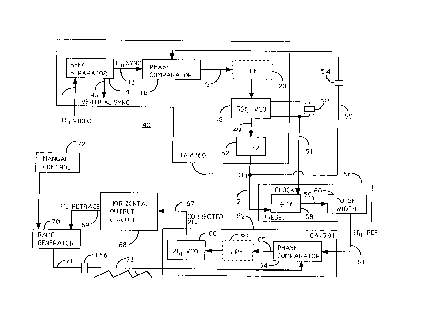
A synchronization system for displaying 1fH video signals at a
5 2fH scanning rate is shown in block diagram form in FIGURE 1, and
generally designated by reference numeral 10. An analog circuit 12,
for example, comprises a sync separator 14, a phase comparator 16
and a voltage controlled oscillator 18 having a 1fH rate output
signal. Voltage controlled oscillator is denoted 1fH VCO. A 1fH
10 video signal is an input on line 11 to sync separator 14. The 1fH
video signal may be a standard NTSC interlaced video signal. The
sync separator 14 provides horizontal synchronizing pulses on line
13 as one input to phase comparator 16 and vertical synchronizing
pulses on another output line, not shown. The output of phase
15 comparator 16 on line 15 is an input to low pass filter 20, denoted
LPF. The error control signal generated by phase comparator 16 on
line 15 is integrated by low pass filter 20 to develop an error
control signal for voltage controlled oscillator 18. The output of
voltage controlled oscillator 18 on line 17 is a 1 fH frequency timing
20 signal. The 1fH timing signal on line 17 is an input to 1fH-to-2fH
converter 22. The 1fH timing signal on line 17 is fed back on line 19
as the second input to phase comparator 16. Phase comparator 16,
voltage controlled oscillator 18 and line 19 form a first phase
locked loop, generating a 1fH rate output signal. The 1fH timing
25 signal on line 17 is phase locked to the synchronizing signals of the
1fH video input on line 11.
A 1fH-to-2fH converter 22 generates a 2fH rate timing signal
on line 23 from the 1fH timing signal on line 17. The 2fH timing
signal on line 23 is an uncorrected timing signal, denoted 2fH-REF.
30 The operation of the 1fH to 2fH converter 22 is explained in more
detail in connection with FIGURE 3.
The 2fH timing signal on line 23 will be symmetrical only in so
far as the 1fH timing signal on line 17 has a perfect, or nearly
perfect, fifty percent duty cycle, and tight tolerance parts are used
35 in the 1fH to 2fH converter 22. As a practical matter, the duty cycle
8 2038778 RCA 85,451
of the 1fH signal may exhibit unacceptable deviation from a fifty
percent duty cycle due to 1fH jitter.
The term 1fH jitter is used herein to refer to a 1fH cyclical
variation of the output of the low pass filter 20, which is the error
5 correction signal for the voltage controlled oscillator 18. The 1 fH
jitter causes a cyclical variation of the output of voltage controlled
oscillator 18, at the 1fH rate. The 1fH synchronizing pulses shown
in FIGURE 2(a) are separated from the 1fH video signal by sync
separator 14. The error signal, or control voltage, shown in FIGURE
1C 2(b) is typical of how the the 1fH jitter can occur. The jitter may
result from feeding back the 1fH timing signal to the phase
comparator. The error control signal gradually decreases over most
of the 1/fH period, which causes the frequency of the 1fH VCO to
gradually decrease during each 1/fH period. The 1fH signal produced
15 by voltage controlled oscillator 18 shown in FIGURE 2(c) is phase
locked to the synchronizing pulses. The frequency of the voltage
controlled oscillator varies to track the 1 fH synchronizing pulses.
The 2fH timing signal~ which is derived from the 1fH signal, has two
pulses for each period of the 1fH signal as shown in FIGURE 2(d). The
20 first 2fH pulse shown has a period tA and the next successive 2fH
pulse has a period tB. Due to the typical variation in the control
signal for the 1fH VCO, the periods tA and tB may not be equal. As
shown in FIGURE 2(c), for example, tA is shorter than tB. Therefore,
the retrace pulses which would result from the uncorrected 2fH- R E F
25 signal have greater amplitudes during the alternate periods tB than
during the alternate periods tA as shown in FIGURE 2(e). An
alternating succession of retrace pulses having different amplitudes
Y1 and Y2 results in the two sets of alternating trace lines having
different starting points, as illustrated in FIGURE 8. The
30 uncorrected timing signal 2fH-REF on line 23 may exhibit
unacceptable asymmetry, which might result in a split raster.
A second phase locked loop is formed by a television horizontal
processor circuit 24, which may be embodied as an industry type
CA1391. Functions in the CA1391 include a phase comparator, an
35 oscillator, a Vcc voltage regulator and a predriver.
2038778
9 RCA 85,451
The 2fH-REF timing signal on line 23, which as noted may be
adversely affected by jitter in the 1 fH timing signal on line 17, is an
input to the phase comparator 26 of processor circuit 24. The
output of phase comparator 26 on line 25 is an input to a low pass
5 filter 30. Voltage controlled oscillator 28 generates a 2fH rate
output signal. The error control signal generated by phase
comparator 26 is integrated by low pass filter 30. The output of
voltage controlled oscillator 28 on line 27 provides a CORRECTED
2fH signal for horizontal output circuit 32. The horizontal output
o circuit 32 generates a horizontal scanning current, and provides 2fH
RETRACE pulses on line 33. The retrace pulses are an input to a
delay circuit 34, for adjusting the phase of the CORRECTED 2fH
signal relative to the uncorrected 2fH-REF timing signal. The
uncorrected 2fH-REF timing signal has a fixed phase relationship
15 with the 1fH timing signal, through the 1fH to 2fH converter 22. The
output of the delay circuit 34 on line 35 is a second input to phase
comparator 26.
The operation of the second phase locked loop is such as to
average period and frequency variations of the pulses in the 2fH-REF
20 timing signal, caused by jitter of the 1fH timing signal. More
particularly, the time constants of the low pass filters of the
respective phase locked loops are set to provide the 1fH phase
locked loop with a slower loop response than that of the 2fH phase
locked loop. The 1fH loop is relatively slow, that is, having a narrow
25 bandwidth to optimize rejection of phase jitter with decreased RF
signal strength, which may be evident in fringe reception areas. The
2fH loop is typically faster, that is, having a wider bandwidth in
order to optimize tracking of variations in the raster scanning
current due to horizontal output transistor storage time variations
30 and high voltage transformer tuning effects. The result is a straight
nonbending raster under all beam current loading conditions. An
exception to this mode of operation is in regard to the compromises
necessary in the 1fH loop to accommodate signals from video
cassette recorders and the like, in which step changes of up to 10
35 microseconds are sometimes encountered. Tradeoffs can be made to
2038778 RCA 85,451
weak signal performance without significant overall degradation of
receiver performance.
If the asymmetry of the 2fH pulses within a given 1fH period is
such that the first of the two pulses in the given 1fH period has a
5 frequency that is too high, the next pulse will have a frequency
which is too low, and vice versa. Referring to FIGURE 2(c), tA + tB is
constant, equalling the 1fH period. The variations of the 2fH-REF
signal will always result in successive error signals of an opposite
sense for each 1fH period. This will be true except in those
10 instances when there happens to be no asymmetry error and no error
voltage in a given 1fH period. The low pass filter of the 2fH loop
will not let the 2fH voltage controlled oscillator change frequency
as fast as changes occur in the error control signal resulting from
variations in the uncorrected 2fH-REF timing signal, which occur at
15 a 1fH rate. By the time the 2fH voltage controlled oscillator
decreases frequency a little, for example in response to an increase
in the frequency of the 2fH-REF timing signal during a period tA the
error signal changes sense to increase the frequency in response to
the subsequent decrease in the frequency of the 2fH-REF signal
20 during the subsequent period tB f the same 1fH period. This has the
effect of driving the error control signal closer to an average value,
which results in a smooth 2fH DRIVE signal. Accordingly, the
CORRECTED 2fH synchronizing signals on line 27 are sufficiently
symmetrical within the period of the 1 fH timing signal to prevent
25 raster splitting. Stated more broadly, the second phase locked loop
is not only effective to lock the CORRECTED 2fH signal to the 1fH
synchronizing signal, the second phase locked loop is effective to
average out the timing errors in the uncorrected 2fH-REF signal due
to 1fH jitter. The timing errors cannot be corrected by employing a
30 phase control loop which does not include an oscillator.
FIGURE 3 illustrates a suitable 1fH to 2fH converter circuit 22,
which may be utilized in the circuit shown in FIGURE 1. The circuit
22 generates a 2fH timing signal on line 23 responsive to a 1fH
timing signal on line 17. Positive pulses of the 2fH-REF output
35 signal on line 23 are generated when transistor Q14 conducts. An
inverted output signal is available at the collector of transistor
203877~
11 RCA 85,451
-
Q15. Conduction of transistor Q14 is controlled by two pairs of
transistor switches, Q10 and Q11 on the one hand, and Q12 and Q13
on the other hand.
The 1 fH timing signal is capacitively coupled to converter
5 circuit 22 through capacitor C2. The effect of capacitor C2 is to
convert each rising edge of the 1fH timing signal to a positive pulse,
and each trailing edge thereof to a negative pulse, as shown by the
waveform on line 21. In the absence of such pulses, the voltage
level at the base of transistor Q12 will be Vcc/2, by the action of
10 the voltage divider formed by resistors R12 and R13. Vcc may be
+16 volts, for example. The quiescent voltage at the emitters of
transistors Q12 and Q13 will be Vcc/2 - Vbe, by reason of the
emitter follower configuration of transistor Q12. The anode of
diode D11 will also be at Vcc/2, and the cathode of diode D11 will
15 therefore be at Vcc/2-Vbe, which voltage appears at the base of
transistor Q13. Accordingly, in this quiescent state, transistor Q12
is turned on and transistor Q13 is turned off. The base of transistor
Q11 will be at Vcc/2 - Vbe due to the voltage drop across diode D10.
The base of transistor Q10, which is also line 21, will be at Vcc/2.
20 The emitters of transistors Q10 and Q11 will be at Vcc/2 - Vbe.
Accordingly, in the same quiescent state, transistor Q10 will be
turned on and transistor Q11 will be turned off. Whenever a positive
voltage spike raises the voltage level at the anode of diode D11 to
Vcc/2 + Vbe, the voltage at the base of transistor Q13 will be raised
25 to Vcc/2, and of sufficient magnitude to turn on transistor Q13. At
the same time, transistor Q12 will be turned off. When transistor
Q13 turns on, the base of transistor Q14 will be pulled to ground,
and transistor Q14 will turn on. When transistor Q14 turns on, a
positive 2fH rate pulse will be initiated at the collector of
30 transistor Q14. When the positive voltage spike on line 17
terminates, the additional voltage across capacitor C2 will be
dissipated at a time constant determined by the values of resistor
R14 and capacitor C2. When capacitor C2 is sufficiently discharged,
transistor Q13 will turn off and transistor Q12 will turn on. When
35 transistor Q13 turns off, transistor Q14 turns off, and the 2fH pulse
is terminated. When a negative voltage spike lowers the voltage on
203~778
12 RCA 85,451
-
line 21 to Vcc/2 Vbe, transistor Q11 will be turned on and
transistor Q10 will be turned off. When transistor Q11 turns on,
transistor Q10 will be turned off. When transistor Q1 1 turns on,
transistor Q14 turns on, and produces another positive 2fH pulse.
5 When the negative voltage spike terminates, and the charge on
capacitor C2 discharges, transistor Q11 will turn off and transistor
Q10 will turn on. When transistor Q11 turns off, transistor Q14
turns off, and terminates the positive pulse. Although the width of
the 2fH-REF pulses on line 23 will be subject to some variation, this
10 variation is of no consequence, as the phase comparator 26, of a
1391 type integrated circuit, is edge sensitive. It is only necessary
that the pulse width of the 2fH-REF pulses be wider than
approximately one-half of the retrace derived pulse, which is the
other input to the phase comparator. This minimum width can be
15 assured by the proper selection of capacitor C2 and resistor R14. At
the same time, the pulse width should be maintained as narrow as is
necessary in order to maintain a fast switching response in the
converter circuit.
A synchronization system for a total 2fH deflection
20 synchronization system is shown in block diagram form in FIGURE 4,
and generally designated by reference numeral 40. The 1-chip
(analog circuit) 12 shown in FIGURE 1 is embodied as an industry
type TA8360 1-chip. A 1fH video signal on line 11 is an input to
sync separator 14. The sync separator 14 provides vertical
25 synchronizing pulses on line 43 and 1fH horizontal synchronizing
pulses on line 13. The 1fH synchronizing signals on line 13, shown in
FIGURE 5(a), are an input to phase comparator 16. The output of
phase comparator 16 on line 15, shown in FIGURE 5(b), is an error
control signal input to low pass filter 20'. The frequency
3 o characteristic of the low pass filter in the TA8360, for example, is
determined primarily by external timing components. Accordingly,
block 2b is shown by dashed lines. The external elements may be a
series R-C network, having a 10 microfarad capacitor and a 3K
resistor coupled between the capacitor and ground. Voltage
35 controlled oscillator 48 operates at a 32fH rate, responsive to a
ceramic resonant circuit 50. A nominal 32fH timing signal on line
13 2038 77~
_
49, shown in FIGURE 5(c), is an input to a divide by 32 circuit 52.
The output of the divide by 32 circuit on line 17 is a 1fH drive
signal, shown in FIGURE 5(d). The 1fH signal is an input on line 55 to
the other input of phase comparator 16, which can result in the error
control voltage of FIGURE 6(b) being adversely modified by a 1fH
ripple as shown. In the event the width of the 1fH pulses, being fed
back to the phase comparator 16, are too wide, the pulse width can
be reduced, for example by series coupled capacitor 54. The 32fH
output of the resonant circuit 50 is also available externally of the
1-chip, on line 51.
A progressive scanning control circuit 56 also provides a
number of control functions. The 32fH output of resonant circuit 50
on line 51 and the 1fH output on line 17 are inputs to a divide by 16
circuit 58. The 32fH signal provides a CLOCK input for circuit 58.
The output of the divide by 16 circuit is a timing signal at a
frequency of 2fH, twice the 1fH rate of the output of the divide by 32
circuit. The 1fH timing signal on line 17 provides a PRESET
synchronizing signal for initializing the counter of divide by 16
circuit 58 and synchronizing the circuit 58 with the 1 fH signal on
line 17. The output of the divide by 16 circuit 58 on line 59 is an
input to pulse width circuit 60. Pulse width circuit 60 assures that
the width of the pulses in the uncorrected 2fH-REF signal on line 61
will be wide enough to ensure proper operation of phase comparator
64 in the CA1391 type integrated phase locked loop circuit 62.
As is the case with the circuit shown in FIGURE 1, the 2fH-REF
signal is symmetrical only to the extent that the initial duty cycle
of the 1fH signal is fifty percent. The effect of the 1fH ripple on the
error control voltage for the 32fH VCO is reflected in the waveform
of FIGURE 5(b). The error control voltage periodically falls during
each 1fH period. Accordingly, the output frequency fvco Of the 32fH
VCO falls periodically, during each 1fH period. As the frequency
falls, each subsequent output pulse from the 32fH VCO has a lower
frequency. As the frequency decreases, the pulse width 1/fvco
increases. The divider circuit 58 doubles the frequency of the 1fH
signal, which has a period of 32 output pulses of the 32fH VCO, by
dividing the period in half, that is, into two sixteen pulse periods.
2038778
1 4 RCA 85,451
However, due to the falling 1fH VCO frequency and due to the
periodically increasing pulse widths, the aggregate width of the
first sixteen pulses, tA is less than the aggregate width of the next
sixteen pulses, tB. When the duration of tA is not equal to the
5 duration of tB, the 2fH-REF timing signal is not symmetric within
the period of the 1 fH signal, notwithstanding the precision of the
digital divider. This asymmetry can cause retrace pulses of
alternating amplitudes Y1 and Y2 as shown in FIGURE 5(f), which are
analogous to the retrace pulses shown in FIGURE 2(e), and which can
10 result in the raster splitting. The 2fH-REF signal generated by the
digital circuit must therefore also be treated as an uncorrected
signal, which requires further processing.
The error control signal of phase comparator 64 on line 65 is
an input to low pass filter 63. The output of low pass filter 63 is a
15 control input to voltage controlled oscillator 66, which operates at
a 2fH rate, and is denoted 2fH VCO. The operating frequency of a
type 1391 oscillator and the frequency response of the low pass
filter are determined by external timing components, as shown in
more detail in FIGURE 7. Accordingly, block 63 is shown by dashed
20 lines. The frequency characteristic of the low pass filter 63 is
determined by the series R-C network formed, for example, by 1.5
microfarad capacitor C53 and 2K resistor R68. The output of voltage
controlled oscillator 66 on line 67 provides CORRECTED 2fH
synchronizing signals for a horizontal output circuit 68. The output
25 of the horizontal output circuit 68 on line 69 provides a 2fH signal
in the form of 2fH RETRACE pulses. The 2fH RETRACE pulses are an
input to ramp generator 70, which is subject to a manual phase delay
by manual delay circuit 72. The output of ramp generator 70 on line
71 is AC coupled by capacitor C56 to the other input of phase
30 comparator 64 by line 73.
The waveforms of FIGURE 6(a) - 6(d) illustrate the relative
phase positions of the 1fH and 2fH-REF timing signals generated in
the circuit of FIGURE 4. FIGURE 6(a) illustrates the 1fH SYNC pulses
separated by sync separator 14 and provided to phase comparator 16
35 on line 13. FIGURE 6(b) shows the 1fH output of the divide by 32
circuit 52 on line 53. The first phase locked loop is therefore
2038778
1 5 RCA 85,451
responsible for maintaining the relative phase of the leading edge of
the 1fH pulses and the midpoint, for example, of the 1fH SYNC pulses.
This alignment can be adjusted by means of a delay or filter circuit,
shown as capacitor 54. As illustrated in FIGURES 6(a) and 6(b), the
5 delay circuit 54 is not inserting any delay. FIGURE 6(c) illustrates
the 2fH-REF signal generated by pulse width circuit 60 on line 61,
which is one of the inputs to phase comparator 64 of the second
phase locked loop 62. As is the case with the circuit of FIGURE 1,
the second phase locked loop 62 of FIGURE 4 is effective to lock the
10 CORRECTED 2fH signal to the 1fH synchronizing signal and is
effective to average out the asymmetric timing errors in the
uncorrected 2fH-REF signal due to 1fH jitter. FIGURE 6(d) shows the
2fH RETRACE pulses on line 69, which are an input to a ramp
generator 70. A manual control circuit 72 for the ramp generator 70
15 enables adjustment of the difference in phase between the
CORRECTED 2fH pulses and the 2fH-REF pulses.
A circuit schematic for a portion of the block diagram shown
in FIGURE 4 is shown in FIGURE 7. Phase locked loop circuit 62 is
embodied as an industry type CA1391 integrated circuit. The circuit
20 62 contains an oscillator 66, phase detector 64, predriver 84, phase
detector output driver 86 and Vcc voltage regulator 87. The
oscillator 66 is an RC type with terminal 7 used to control
frequency. An external capacitor C51 is connected from terminal 7
to ground and charges through external resistance R62 coupled
25 between terminals 6 and 7. When the voltage at terminal 7 exceeds
an internal potential bias, capacitor C51 is discharged through an
internal resistor. This conduction causes generation of a drive
pulse, which terminates when the capacitor is sufficiently
discharged. The discharge cycle is responsive to a sawtooth signal
30 at terminal 4. Negative-going synchronizing pulses at terminal 3
are phase compared with the sawtooth waveform at terminal 4,
which is derived from horizontal flyback or retrace pulses. If there
is no phase difference between the synchronizing signal and the
sawtooth waveform, there is no net output current at terminal 5.
35 When a phase offset occurs, current flows either in or out of
terminal 5 to correct the frequency. The duty cycle, or mark space
2038778
1 6 RCA 85,451
ratio, of the predriver 84 may be adjusted by setting the potential at
terminal 8. In the circuit of FIGURE 7, this is determined by the
voltage divider formed by resistors R63 and R64. Potentiometer
R37, coupled to terminal 7 through resistor R72, may be used to
5 manually adjust the frequency of oscillator 66.
The ramp generating circuit 70 comprises transistor Q4,
resistor R55 and capacitor C50. The ramp signal generated across
capacitor C50 is AC coupled to terminal 4 through capacitor C56. A
transistor Q2 and potentiometer R20 form a manually operable delay
10 circuit 72, which varies the current needed to charge the ramp
capacitor C50. Variation of the time needed to charge capacitor C50
provides a variable delay of approximately from 0-2 microseconds in
the relative phase of the 2fH-REF pulses and the CORRECTED 2fH
pulses.
The CORRECTED 2fH output of predriver 84 on line 67 is an
input to a push-pull driver circuit comprising transistors Q5 and Q6,
which provides a 2fH DRIVE output signal to the horizontal output
circuit.