Note: Descriptions are shown in the official language in which they were submitted.
~33~
~IG~ 8P~D PROCF880R ~OR DIGITAL 8IGNA~ P~OCE~8ING
F~el~ Of ~he I~v~ntio~
The present invention is directed generally to
digital signal processing applications and, more
particularly, to a high speed processor (HSP) module
for digital signal processing (DSP) in real time
applications wherein the HSP is implemented on a
programmable platform.
REhATED APPLICATIONS
The following applications are included herein
by reference:
(1) assignee's copending application, Serial
No. 07/1~2,79~, DIGITAL MAP SYSTEM, filed May
11,1988:
~2) assignee's copending application, docket
number 89277 filed on the same date as the present
invention entitled POLYGON TILING ENGINB;
(3) assignee's copending patent application,
Serial No. 07~419,722, PARALLEL POLYGON/PIXEL
RENDERING ENGINE ARCHITECTURE FOR COMPUTER GRAPHICS,
filed October 11, lg~9;
(4) assigne~'s copending patent application,
~3,~2
docket number 89278, filed on the same date as the
present invsntion entitled POLYGON SORT ENGINE:
(5) assignee's copending patent application
docket number 89683, filed on the same date as the
presant invention entitled THREE DIMENSIONAL
COMPUTER GRAPHIC SYMBOL GENERAroR; and
(6) assignee's copending patent application
docket number 88514, filed on the same date as the
present invention, entitled METHOD AND APPARATUS FOR
0 GENERATING A TEXTURE MAPPED PERSPECTIVE VIEW.
BACRGROUND OF THB INVENTION
Implementing digital imaging algorithms in real
time is hardware intensive. Specific hardware
solutions as found in the prior art are inflexible.
Other solutions that combine pipeline hardware with
programmability tend to fall shor~ of desired
throughput capabilities for high speed applications.
Algorithm specific DSP devices, such as the model
number UT 6g532 as manufactured by United
Technologies Micro Electronics Center of Colorado
Springs, Colorado provide partial solutions to the
problem of real time imaging. The model UT 69532's
pipeline architecture provides some flexibility and
achieves a throughput ratP of about 75 MF10PS peak.
The present invention makes use of high ~peed
`--" 2~3382~
gallium arsenide (GaAs) very large scale integrated
circuits mounted on a thin film multilayer (TFML)
multichip package. The architecture as provided by
the present invention allows the DSP algorithms to
be performed at high speed while also providing
capabilities to interface to other components of a
digital map graphic display system at low speeds.
This invention can achieve 400 MFLOPS peak
performance which is a significant improvement over
prior art devices.
8UNNARY OF T~B INYE~ION
Figure 1 shows a block diagram of the major
components of a high speed graphics display system.
These include a means for display 50, a video
generator means 40, a raster engine means 30, a
polygon sort engine means 100, a polygon tiling
angine means 20 and a high speed numeric processor
10. The high speed numeric processor comprises a
high speed processor as provided by the invention
which fits architecturally near the beginning of the
pipeline to feed vertices to the polygon tiling
engine. The polygon sort engine 100 is designed to
receive polygon vertices from the polygon tiling
engine and correctly load these vertices into the
raster engine. The raster engine, in combination
... . . ..
` ~= 2~3~s~
4 --
with the video generator, renders three dimensional
raster graphics on the video display 50.
The present invention comprises a high speed
processor (HSP) including a processor interface, an
output pipeline interface, an input pipeline
interface, and a multichip floating point processor.
The floatinq point processor further comprises a
data register file memory, a coefficient register
file memory, a floating point multiplier-
accumulator, a microsequencer and a control storerandom access memory (RAM). The high speed
processor provided by the present invention is
capable of operating at a clock rate of about 200MHz
with the floating point processor capable of 400
MFLOPS peak performance.
In one embodiment of the invention, the HSP is
entirely self contained in a TFML package with all
high speed interfaces residing on the package
substrate and only C-MOS speed interfaces residing
off of the FPP package. The FPP comprises five GaAs
integrated circuits consisting of a floating point
multiplier-accumulator (MACC), a plurality of multi-
port register file memories (RFM), RAM for
microprogram storage and a clock generator.
In one aspect of the invention, a 50 step
,~ ' ' . , , . , . ,,' ,, ' ' .
2 ~
- 5 -
algorithm running at 200 MHz can be executed 4
million times per second. This matches well with
the individual input and output data rates of about
5~z. In another aspect of the invention, requiring
simultaneous input and output, a lOMHz interface has
been provided.
It is one object of the invention to provide a
flexible solution to a wide variety of digital
imaging problems wherein an HSP can perform 32 bit
IEEE standard operations, including multiply, add
and subtract operations, for example, at 200 MFLOP
peak throughput.
It is another object of the invention to
provide a high speed processor with low speed
input/output ports for in~erfacing with a minimal
impact on graphics system hardware.
It is yet another object of the invention to
provide a high speed processor having a debug
interface which provides a low speed means of
debugging microcode.
Other objects, features and advantages of the
present invention will become apparent to those
skilled in the art through the Description o~ the
Preferred Embodiment, Claims, and drawings herein
wherein like numerals refer to like ~lements.
- , ~ . . - , .
` ` 2~38~2~
BRIEF DESCR:I:PTION OF THE: DRAWING8
Figure l is a block diagram of certain major
components used in a high speed graphic display
system including the high speed processor or the
in~ention.
Figure 2 is a block diagram of one example
embodiment of a high æpeed processor as provided by
the instant invention.
Figure 3 is a block diagram of the floating
point processor as employed in one aspect of the
invention.
Figure 4 is a more detailed block diagram of a
microsequencer as employed in one aspect of the
invention.
Figure 5 is a more detailed schematic diagram
of a floating points multiplexer-accumulator as
employed in one aspect of the invention.
DE8CRIPTION OF THE PREF~RRED ~MBODIMENT
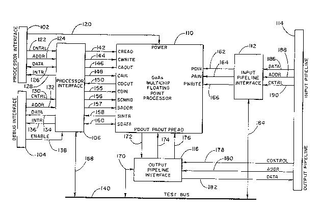
Referring now to Figure 2, a block diagram of
one example embodiment of a high speed processor as
provided by the instant invention is shown. The
high speed processor comprises a first processor
interface 102, a debug interface 104, a second
processor interface 106, a floating point processor
(FPP) llO, output pipeline interface 116, input
.~ ~ 3 ~
- 7 -
pipeline interface 112 and input/output pipeline
connector 114. The processor interface 106 provides
a means to control the FPP in the host environment.
In an airborne digital map application of the
invention, control registers, micro-code, and
pertinent data can be loaded and updated in a real
time flight environment from a Digital Map Unit or
other on-board computer. This capability is needed
since coefficients for a given algorithm will change
~ith environmental dynamics, such as aircraft
dynamics.
The debug interface 104 provides a means for
performing software debug functions. Break points,
single step, and internal memory access are provided
in the sequencer to accommodate debug of micro-code.
This functionality is vital since the high speed
nature of the GaAs components makes conventional
debugging techniques impractical.
The pipeline interface 112 provides a path for
passing a high volume of data, which i~ operated
upon by the high speed processor. Digital map
system architecture is described in the assigneels
copending patent application entitled METHOD AND
APPARATUS FOR GENERATING A TEXTURE MAPPED
PERSPECTIVE VIEW, filPd on the same date as this
. . -
~3~2~
application and incorporated herein by reference.
Such architecture is highly pipelined, requixing
processing of multiple data points through identical
operations. The pipelins interface allows the data
to pass through the FPP with a minimal amount of
intervention by the control processor. As explained
in the texture map application, the control
processor has been successfully implemented as a
1750A processor in certain embodiments of the
invention.
As can be seen in Fi~ure 2, various control
signals, addresses and data are interchanged between
the high speed processor and the rest of the
graphics pipeline system. Processor interface 102
includes conductor 120 for supplying power to FPP
110. Also passed through the first processor
interface 102 to the second processor interface 106
are the following signals: CNTRL, ADDR, DATA and
INTR on linas 122, 124, 126 and 128, respectively.
Debug interface 104 passes signals CNTR, A~DR, DATA
and INTR on lines 130, 132, 134 and 136 to the
second processor interface 106. Debug interface 104
also provides an enable on line 138 to the second
processor interface 106. Multichip floating point
processor 110 includes the following inputs xPceived
` -
_ 9 _ ~3~ h
from processor interface 106: CREAD on line 142,
CWRITE on line 144, CAOUT received on line 146, CAIN
received on line 148, CDIN received on line 155,
SCNND on line 156, and SADDR received on line 157.
FPP 110 also outputs signal CDQUT on line 150 to the
second processor interface 106. FPP further outputs
signal SINTR to the second processor interface 106
on line 158. The second processor interface 106
communicates with test bus 140 via conductors 168.
Output pipeline interface 116 communicates with
the output pipeline section of connector 114 through
control signal CONTROL on line 178 and address
signal ADDR on line 180. The output pipeline
interface 116 outputs data to the output pipeline on
line 182. The output pipeline interface 116 is
connected to the test bus 140 by input/output lines
170. Output pipeline interface 116 is also
connected to the FPP 110 and supplies inputs PAOUT
on line 174 and PREAD on line 176. FPP 110 supplies
20 PDOUT on line 172 to the output pipeline interface
116. Input pipeline interface 112 communicates with
test bus 140 via line 184. The input pipeline
interface provides signals to inputs PDIN, PAIN and
PWRITE on lines 162, 164 and 166, respectively, to
the FPP 110. FPP interface 112 receives data from
.. ',. ~
-
- -.: ~ . , : ~
~ ;: :~, . . .
!,
' ' '
~3~ 2~
-- 10 --
the input portion of pipeline 114 on line 186.
Address data ADDR is input via lines 188 and control
signal CNTRL is presented to the input pipeline
interface on line 190.
The debug interface 104 is designed into the
FPP to allow external control of the FPP at full
clock speed. In one example of an embodiment of the
invention, the FPP is implementad as a GaAs
multichip application specific integrated circuit
(ASIC). The debug interface operates at about 10
MHz and controls the high speed circuitry. Debug
software, which is executable on a personal
computer, is used to develop FPP firmware and debug
it through the debug interface In addition, a
software simulator of the FPP may be used
advantageously to allow non-real-time debug FPP
firmware. The debug routines and firmware to be
debugged depend upon the application and may be
implemented using well known tachniques.
Referring now to Figura 3, a more detailed
block diagram of the floating point processor 110 as
provided by the invention is shown. The floating
point processor comprises six major fun~tion blocks.
The function blocks include identical register file
memories (RFMs), namely, a data RF~ 200 and a
coefficient RFM 204, a microsequencer 206, a
floating point multiplier-accumulator (MACC~ 201 and
control store RAM 208. The microsequencer 206
contains all state and control circuitry required by
the processor. The control store RAM holds the
microcode executed by the microsequencer. The MACC
includes a floating point multiplier and floating
point accumulator (described with reference to
Figure 4) which perform the processor's arithmetic
operations. The FPP interfaces with first high
speed interface 240 called A-BUS and second high
speed interface 242 called B-BUS as well as high
speed input bus 250 called R-BUS.
In one example embodimènt of the invention, the
RFMs comprise 5 port 256 x 32 RAMs. The RFMs 200
and 204 each have two high speed outputs namely 220,
222, 224 and 226, respectively. Each of the RFMs
has one high speed input. RFM 200 has high speed
input 214 for receiving PIPELINE IN data and RFM 204
has high speed input 218 for receiving signals from
the coefficient input bus called COEFF IN BUS. Each
RFM has one output and one input tied to R-BUS 250.
In one embodiment of the invention, the A-BUS port
includes 8 pins for accommodating 8 bits of address
data, 32 pins fcr accommodating 32 bits of data
:- ~ . ., , , ::,, ,
~ ~ $ 3 ~
- 12
using a tristate output and one pin for
accommodating a read strobe control signal. The B-
BUS port is similarly configured. The R-BUS port is
configured for high spaed input and preferably
includes pins to accommodate 8 bits o~ address input
data, 32 pins to accommodate 32 bits of data and 1
pin to accommodate a write strobe.
The microsequencer 206 provides control and
decision making logic for the FPP. Additionally,
the sequencer provides address generation for the
other components of the FPP. Part o~ this address
generation circuitry includes an indexed addressing
mode which accommodates software loops. Each
address field, namely A, B and R, contains a bit to
enable this indexed mode. The index bit acts as a
count enable to the address generation circuitry for
the duration of the loop. Exiting from the loop
will disable the count and cause any new addresses
to be loaded. The size and increment is controlled
by a step sized register ~one per address field).
The length of count is controlled by a count
register or alternately by a condition code inputO
The microsequencer 206 provides an interface to
the host environment via the sequencer interface.
This interface provides a means to access sequenrer
,3 ~ ~ ~
~ 13 -
status and control registers and to access or modify
control store RAM 208. Additionally, this interface
provides the debug facilities for the FPP. Through
this interface, the sequencer can be made to halt on
an address or single step through control store RAM.
The microsequencer executes and makes decisions
based upon a microcode stored in control store RAM.
Following is a list of microsaquencar instructions
which may advantageously be implemented in one
example of the invention:
1) LOAD REGISTER
a) Load count register
b) Load A address, step register
c) Load B address, step register
d) Load R address, step register
e) Load stack pointar
f) load program counter
g) load A, B, or B offset register
h) load A and B offset register immediate
2) LOOP ~ADDRESS> - Jump to the specified address
and decrement the count register (CR) If CR = O
do not jump. Increment all enabled address
counts upon jump~
3) JUMP <ADDRESS>
a) Jump unconditionally
b) Jump on Zero
c) Jump on greater than
d) Jump on less than
e) Jump on overflow } options
f) Jump on widest flow ~ options
4) CALL <ADDRESS>
5) RETURN
6) CONTINUE - Sequence to next address. Normal
. : . :: - -- ~, -.: : , ,.
. . . , ., ~ . : :
~ ,, ::
.-. ,.. . . . : : .
2 ~3 ~ ~h 2
- 14 -
operating mode when issuing MULT, ADD and RFM
command with no sequencer loop or load.
The call and return command require that a
small stack be maintained within the sequencer to
hold old program counter and register values.
Following is a list of sequencer registers:
a) Program counter register ~10 bits)
b) Stack pointer register (8 bits)
c) Loop count register
d) A address step register t8 bits)
e) B address step register (8 bit~)
f) R address step register (8 bits)
g) Sequencer control register
h) Sequencer status register (Read Only)
i) A address base register (8 bits)
j) B address base register (8 bits)
k) R addres~ base register (8 bit5)
1) A address offset register (8 bits)
m) B address offset r2gister (8 bits)
n) R address offset register (8 bits)
Referring now to Figure 4 with continuing
reference to Figure 3, a more detailed block diagram
of the microsequencer 206 as used in one embodiment
of the invention is shown. The microsequencer
comprises sequencer interfac~ 300, condition code
interface 302, command interface 304, sequencer
state machine 306, saquencer register 308, control
store RAM interface 310, and address generator 312.
The sequencer interface receives command word RST to
reset the sequencer on line 260. SCMD is
advantageously a 4-bit command word which is input
on line 252 into the sequencer interface 300.
Address data S ADDR, in this example a 12-bit word,
.; ,; . , ~
.. ...
8 ~
- 15 ~
is input on line 254 to the sequencer interface. A
16-bit data bus with sequencer data S DATA is ported
on conductors 256. Sequencer instructions are
transmitted on conductors 274 which, in this
example, comprise conductors capable of carrying 24
bits or information divided into sequencer
instructions labeled SEQINSTR, which in this
example, is a 6-bit instruction carried on lines
274A. The remainder of lines 274 are labeled lines
274B and carry instruction addresses labeled INSTR
ADDR which are input into the command interface 304.
The address generator 312 outputs command A-ADDR on
line 262, B-ADDR on line 264 and R-ADDR on line 266.
A-ADDR is, in this example, a 9-bit word comprising
the destination address sent to the A port of the
RFMs. B-ADDR is, in this example, a 9-bit address
sent to the B ports of the RFMs. Similarly, R-ADDR
is, in this example a 9-bit address which represents
the R-BUS destination address.
The command interface 304 functions to receive
seguencer instructions and the address field for the
instructions from the control store RAM (CSR) 208.
The command interface interprets the se~uence
instructions and the instruction addresses and
provides appropriate inputs on line 320 to the
. - . - . ~- ~ : .:
. . ~ ..
::~ ~ . :: . .
- 16 -
sequencer state machine and line 322 to the
sequencer registers. Following are operation codes
and address field assignments as used in the command
interface in one example of the invention.
- .
17
_ o a a æ a
X s: a a- a-
X a~ aNaN a~
x ~ ~~ ~ a~
X ~ a ~ a aU~
x u~~u a~ à $ à ~ à
E- X ~ a'' X a ~ a~ X a~
a X a~ ~ a~ ~ a~ a~
X ~1 i X O X `~ X ~ X
~ X ~ X ,~
x ~ x ~ ~c ~ x ~ X
a ~ x ,~ X~ X ^ x
o o,, O :,~ O :,, .~ ~ ~
O o o '~ o o
'~ o o o o
o o o o
o o o o
o
,~
- ~ . . ,. : , ~, , ,.. , ,.. :.: : - -
. ~ , - , .,. . ~ ,
... . . .. . .. . ..
18
~ ~ 3 ~
a a ~ æ a
~- ai`'a-
* a~ N a~
a~ O a~ -- =-- ~ a'
a' ~ a~ ,', a 0 a~
X ~ X ~ ~ X X
x O x m ~ u~ x ~' x
o x ~; x ~ ~ '¢ x a~ X
p~ X ~ X ~ ~ X ,~ X
X ,~ X ,¢ ~O , 1 X ~ X
X X ~s ~ ^ X ~ ~C
o ~ O ~ ~0 ~ O
~, o
O O ~;, O .,
o o O O O
o O o o
O
~I
: : . , ~ , . ~. .. -
, .
19 ~ 2
a a a a æ
a- a- a- a
a~ a~ C~N
a~ a~ a~ fi' a
_ a~ a~
~ QU~ a ar~ caa au~ ~ ^
_ ~ -- a~ ~ a~ à ~ a
s~ a~ a~
X ~ X ~ X P~ Q' ~ a~
p: X 1~ ~ ~ X 3 X ~ X
K X c> X x û X a X
x ~ X x X ~ x
x -- x ,î X
~ ~ o o
o o
~ O
o o o ,~ .
o o O o
:.
3' 2
a a a a æ
a- a- a- a- a-
aN aN aN aN aN
a~ a~ c; c;~ a~
a~ a~ a~ a~ ~
au~ a~ ,~ au~ - an ~ ci`
N à E~ ~o S a~ ~ a~
a`~ ~ .c a~ ~ a`
, a~ L, a~ ~ a~
a) a~ a` u~a` ~ a~
O xO x ~ x ,~ x o x
x x ~ x ~ x ~ x
x~ x ~ x o x x
x 1~ x o~ x~ x ~ x
x ~ x ~ x 1, x i, x
~1 x ,~ ~ ~, x x _ x
X X ? X ? X ? X
X X -~ X X X
,~ o ~1 o ~1
o ~ ,1 o o
O O O r~ ~1
,~ ,1 ,1 ,1 ,~
o o o o o
_
U) ,~
.
'. :. : ` `
- : : ... ` ` - ;: `
::
- -
~o ~o
c~ ~ x
Cl ~J X
~ ~ x
~ ~ x
- ~u~ ~ x
à X
3c~ ~ _ x
a0 ~ X
a~ X
X ,~ x ~ x
~: X ~ ~ x
n. ~ X ~ X
x ~1~ X ~ X
1~ x x x
-- x x ~C
x X O
X X O
o o
~1 o
_ o
~1 o
,~ o
o ~1
I
.-
! (3 ~ 2 2
-- 22 --
The sequencer interface 300 receives andinterprets commands from the host environment. It
is a low speed interface used primarily for setup
or debug purposes. The sequencer interface
provides a low speed window into the high speed
environment of the FPP. The following list is a
list of sequencer interface functions as provided
in one example of the invention:
a) Read-Write internal register,
b) Read-Write to control store RAM,
c) Halt on address,
d) Step on cycle, and
e) Halt.
These functions are implemented using known
techniques through a combination of control
register bits and sequencer commands. One example
of signal implementation for each of these commands
ls shown in Table 1 below.
.
23
t~ ~ r;~ ~J
~ U~
O U~ ~n
h
$ ~ ~ ~ '1~
, O O Q~ O
a a ~ a
~ -- -- -- -- -- -- -- -- --
u~
x x x x o o ~ x
r~ o
u~ o x ~l ~l o o o o ~l
r~
O X O O ~1
u~
~ x ~l o o o o o o o
~ x ~c o ~ o ~ o ~l
aJ
o o ~
o ~ p~ u u~
o ~ o ,~
~ ~ ~ x ~ x ~ ~ ~ ~y ~
o o
z; z; ~ ~ 3 m ~; m ~ m ~ m u~
o U~ -~
. ~. .
; . ., . . -
3~
- 24 -
The condition code interface 302 receives
condition codes from the floating point multiplier-
accumulator and passes them as state inputs to the
sequencer state machine. Some o~ the condition
codes used in the condition code inter~ace include:
a~ GREATER THAN,
b) LESS THAN,
c) EQUAL TO,
d) ZERO,
e) OVERFLOW,
f) UNDERFLOW, and
g) NAN (Not a Number).
The control store RAM or CSR interface 310
provides the address and data interface to the CSR
208. Address information is supplied to the CSR
interface via the sequencer interface on line 330
or from the self-contained program counter. The
program counter 311 may be preloaded from the
sequencer registers, CMD interface or sequencer
interface 300.
The address generator 312 provides internal
addressing to and from the RFMs. It is in
communication with the sequencer registers via
lines 332 and the sequencer state machine via lines
334. The sequencer state machine provides state
control as well as control strobes to other
elements in the FPP, including the sequencer
interface, condition code interface, command
~ 25 - ~ ~38~2~
interface, sequencer registers, address generator
and CSR interface.
Referring now to Figure 5, a more detailed
block diagram of the floating points multiplier-
accumulator (MACC) 201 is shown. In one example ofthe invention, the MACC implements IEEE 754 - 1985,
standard floating point arithmetic. The MACC
comprises an A-DATA multiplexer 402, a B-DATA
multiplexer 404, a third multiplexer 406, a fourth
multiplexer 408, and a fifth multiplexer 410.
Further included in the MACC are an address decoder
ADDR-DEC 412, first register file 414, a second
register file 416, an instruction decoder and state
machine 418, a conversion means 420, a multiplier
unit 422, an accumulator 424, a sixth output
multiplexer 426, and a result register 428. These
elements are structured and arranged in accordance
with well-known computer architecture techniques to
operate as a floating points multiplier-
accumulator.
In operation, the MACC is able to convert frominteger to floating point and floating point back
to integer formats. It is designed to accept data
in any of these formats, operate on the data and
output the result in any of the aforesaid formats.
- 26 -
The accumulator can receive inputs from the
multiplier unit 422 on line 430 or its own output
on line 432. This arrangement allows for
accumulate, multiplying and accumulate, and
multiply and add instructions.
This invention has been described herein in
considerable detail in order to comply with the
Patent Statutes and to provide those skilled in the
art with the information needed to apply the novel
principles and to construct and use such
specialized components as are required. However,
it is to be understood that the invention can be
carried out by specifically different equipment and
devices, and that various modifications, both as _o
the e~uipment details and operating procedures, can
be accomplished without departing from the scope of
the invention itself.
What is claimed is:
- ~ : : . . :
: : . , ,, . . ~