Note: Descriptions are shown in the official language in which they were submitted.
2 ~
Case No. ~9040
TRANSIENT FRE~ HIG~ SPEED COIL A~TIVATXON CIRCUIT
Backqround and Summary of tha ~nvention
The present invention relates generally to
noncontact sensors and to an apparatus and method for
selectively energizing and de--energizing inductors in a
system which enables the use of low cost digital
circuitry to provide a transient free output waveform.
The invention may be used in a switched complementary
sensor coil application in which the coil inductances
vary in response to position of a moving member.
Noncontacting sensors typically consist of two
or more tunable inductors each. Although circuit
configurations vary, usually the tunable inductive
element is connected alternatively to a capacitor to form
a resonant tank circuit. Typically, two complementary
inductor coils are used in a switched arrangement.
In the conventional switched arrangement a
first coil is connected to the tank circuit and energized
while a frequency measurement is taken. Thereafter, the
first coil is disconnected and a second coil is
simultaneously connected to the tank circuit where a
second frequency measurement is ta~en. Switching from
one coil to the other in this fashion using digital
switching techniques results in transients, which are a
source of error. This includes an arrangement whereby
the coils are multiplexed at a task repetition rate.
The present invention provides a substantial
transient reduction during coil switching using a
staggered coil activation technique. The technique
allows the coils to be multiplexed after no longer ~han
~3~ ~-3 ~ ~.
Case No. 890~0 2
one period, affording a system with much better frequency
response than is possible using conventional switchiny
techniques. The invention is well adapted to
implementations usin~ low cost, high speed digital
components. The staggered technique offers a system
which is quite tolerant to variations in signal
propagation delays common in digital circuit components.
In other words, unlike conventional switching techniques,
the invention is able to properly function even if the
signal for energizing the first coil and the signal for
de-energizing the second coil propagate through different
circuit paths and therefore have different arrival times.
The present inventive method may be used to
indicate the inductance of a system of inductors which
includes a first inductor and a second inductor, for
example. The inductance may be correlated to a measured
parameter such as position of a tuning sluy or tuning
plate. Hence, the invention is applicable to a wide
range of different parameter sensors.
The method comprises coupling the first
inductor to a tank circuit and thereafter supplying
energy to the tank circuit to causs oscillation at a
first resonant frequency which is determined at least in
part by the first inductor. A waveform indicative of the
first resonant frequency is produced in this fashion.
Next, the second inductor is coupled to the tank circuit
without decoupling the first inductor from the tank
circuit, resulting in a coil overlap period. Thereafter,
the first inductor is decoupled from the tank circuit,
without decoupling the second inductor. Energy is then
supplied to the tank circuit to cause oscillation at a
second resonant frequency which is determined by the
second inductor followed again by a coil overlap period.
A waveform indicative of the second resonant frequency is
thus produced. The waveforms indicative of the first and
~ ~ 3 (~
Case No. 89040 3
second resonant frequencies produced in this fashion are
indicative of the coil inductance.
The invention affords numerous advantages over
conventional switching techniques. It ensures that at
least one coil is always connected in the tank circuit,
thereby avoiding errors resulting from discontinuities.
Only one coil changes status at a given time, never both
at once allowing for smooth transitioning. Further, the
coil being read is not subject to change during its
entire measurement cycle, allowing a transient free
measurement. Also, by connecting both coils together
between individual coil reading cycles all transients are
absorbed.
For a more complete understanding of the
invention and its further objects and advantages,
reference may be had to the following specification and
to the accompanying drawings.
Brie~ Deccription of the Drawings
Figure 1 is a schematic block diagram of a
first embodiment oE the invention;
Figure 2 is a series of waveform diagrams
depicting the operation of the embodiment of Figure l;
Figure 3 is a schematic block diagram of a
second embodiment of the invention;
Figure 4 is a series of waveform diagrams
illustrating the operation of the second embodiment of
Figure 3; and
Figure 5 is a generalized schematic block
diagram of the invention.
De~cription of the Preferxed Embo~iment~
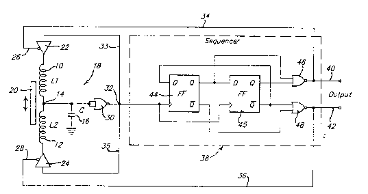
ReEerring to Figure 1, a first embodiment o~
the invention is implemented using a first inductor 10
and a second inductor 12, joined at node 14 and connected
~ ~ 3 ~
Case No. 89040
to capacitor 16 to define a tank circuit, designated
generally at 18. A moving vane tuning plate or slug 20
alters the inductance of inductors 10 and 12 in a
complementary fashion. Movement of the tuning plate in
one direction increases the inductance of inductor 10
while decreasing the inductance of inductor 12. Movement
in the opposite direction has t:he opposite effect, namely
increasing the inductance of inductor 12 while decreasing
the inductance of inductor 10. Each inductor is coupled
to a tristate buffer 22 and 24. The buffers function as
electronically actuated switches. The tristate buffers
switch between a high impedance (open circuit) state and
a low impedance (closed circuit) state in response to
signal.s on the respective control terminals 26 and 28.
In the closed circuit state, the associated inductor coil
is connected to the output of NOR gate 30 at node 32. In
the open circuit state, the associated inductor is
effec~ively disconnected from the circuit.
NOR gate 30 operates essentially as an
oscillator with the resonant frequency of tank clrcuit 18
determining the oscillation frequency. Feedback on
lines 33 or 35 establishes the oscillation condition.
The output of NOR gate 30 at node 32 i.s
connected to the sequencer unit 38 which provides output
signals at terminals 40 and ~2 and which also provides
the control signals via lines 34 and 36 to control
terminals 26 and 28. The sequencer may be constructed
using a relatively simple digital circuit consisting of
a .small number of digital circuit components as well as
programmable array logic (PAL) technology, suitably
programmed microprocessor circuits or the like. For
illustration purposes sequencer 38 has been shown in
Figure 1 as comprising flip-flops 44 and 45 and NOR
gates 46 ancl 48. The basic function of sequencer 38 i~;
Case No. 89040 5
to stagger the selection of inductors 10 and 12 in an
overlapping, "make before break" configuration.
For a better understanding of the operation of
sequencer 38, refer to Figure 2. Figure 2 depicts
inductors 10 and 12 and capacitor 16 in a sequence of
different states of interconnection over different time
intervals. Specifically, Figure 2 depicts one
measurement cycle comprising time intervals I-IV. During
the time interval designated I inductors 10 and 12 are
connected in parallel, with the parallel combination
connected in series with capacitor 16 forming a tank
circuit. The inductors are in an overlapping state
during the time interval I. In time interval II
inductor 10 is connected in series with capacitor 16 in
the tank circuit, but inductor 12 is not. In this second
configuration only the inductor 10 contributes to the
resonant frequency of the tank circuit. In time interval
III both inductors are again connected in parallel and
thus represent the same state as illustrated in time
interval I. In time interval IV inductor 12 is connected
in series with capacitor 16, while inductor 10 is
disconnected. In this state only inductor 12 contributes
to the resonant frequency of the tank circuit.
For convenience the status of inductors 10 and
12 ("Coil Status") for each of the time intervals is
stated as either ON or OFF, ON meaning operably connected
to the tank circuit and OFF meaning operably disconnected
from the tank circuit. As seen from Figure 2 each
inductor is selectively activated and deactivated to
produce the staggered relationship of the invention. The
transitions from activated to deactivated states occur at
the times indicated as "Transition."
By activating the inductors in this fashion
discontinuit:ies and switching transients are eliminated.
This can be seen by monitoring the waveform across
. .
- 2 ~
Case No. 890~0 6
capacitor 16, which is also shown in Figure 2. It is
seen that the frequency of oscillation for any given tlme
interval depends upon the total inductance at that time
connected to the tank circuit. In this regard, assuming
no movement o~ tuning plate 20 occurs between tlme
intervals I and III, the frequency or period of
oscillation at intervals I and III will be identical.
The frequencies or periods at time intervals II and IV
will depend upon the actual inductance values of
inductors 10 and 12, respectively.
In practice, inductors 10 and 12 are
complementary. If L1 and L2 are the inductances of
inductors 10 and 12, respectively, and if L0 is the
inductance of both inductors when the tuning plate is at
symmetry with respect to the inductors, and if QL is the
change in inductance due to movement of the tuning plate
from the symmetry point, the following relationships
exist:
Ll = L0 + QL
L2 = L0 - QL.
When the two inductors are activated in parallel (as
during time intervals I and III) the equivalent
inductance Le is as follows:
Ll ~ L2 ( LO +~L ) ~ ( LO -~L ) ~ ) Z- ~ ~L ) Z LO ~
L2 Ll + L2 ( LD +~L ) +( LD -~L ) ~L ~ L -
For relatively small changes in inductance with respect
to the nominal inductance at the symmetry point, namely
for relatively small QL/LO (i.e., up to 0.05 at full
scale) the value of Le can be approximated by:
Le ~ L0/2.
3 ~
Case No. 89040 7
As can be seen, Le is independent of ~L for relatively
small ~L/L0 and remains constant irrespective of the
position of the tuning plate. This makes it possible to
obtain coil overlapping pexiods which have a fixed
duration throughout the operating range.
NOR gate 30 is configured as an oscillator
which provides a digital output illustrated at
"Oscillator Output" in Figure .'. The frequency and pulse
width of the Oscillator Output is related to the waveform
across capacitor 16 illustrated above the Oscillator
Output in Figure 2. The output of sequencer 38 on
terminals 40 and ~2 is shown at the bottom of Figure 2.
It is seen that the Osci]lator Output at terminal 40 is
high during the interval when inductor 12 is ON and the
output at terminal 42 is high when inductor 10 is ON.
The duty cycles of the output pulses on terminals 40 and
42 correspond to the period of the oscillation waveform
across capacitor 16. The period of the waveform is
dependent on the resonant frequency of the tank circuit,
which is in turn dependent on the inductance of the
selected inductor. Hence the duty cycles of the pulse
outputs on terminals 40 and 42 provide an indication of
the inductance of the associated inductor coils.
The embodiment illustrated in Figures 1 and 2
the coil status switches state with each complete cycle
of the waveform oscillation across capacitor 16. That
is, transitions occur at alternate zero crossings (A, B,
C, D ~ If dQsired, switching can occur after a
greater number of cycles, or after completion of only a
partial cycle, or switching may be tied to an external
clock which is not necessarily related to the frequency
of tank circuit oscillation. Figures 3 and 4 depict an
embodiment of the invention where switching occurs every
half cycle.
2 ~ 3~ J 1
Case No. 89040 8
Referring to Figure 3, the circuit of Figure 1
has been modified to switch on every half cycle by using
the sequencer 38a as illustrated. Specificall~, the
sequencer 38a employs flip-flop 44 and NOR gates ~6 and
48 connected as shown. Sequencer 38a provides output
terminals 40 and 4~ and a center terminal 50 whlch is
derived from the /Q output of flip-flop 44. The
operation of the circuit oE Figure 3 is shown in
Figure 4, which shows two consecutive measurement half
cycles comprising time sequences I-IV and which conveys
similar information to that of Figure 2. The signals on
terminals ~0 and 42 are simi:Lar to those of Figure 2.
The signal on center terminal 50 is a variable duty cycle
output. Note that the Oscillator Output tat node 32)
comprises a series of fixed duration pulses with variable
spacing.
While the invention has been illus~rated using
two examples, one switching every full cycle and another
switching every half cycle, the invention may be
implemented in other ways, as well. Figure 5 depicts a
more generalized circuit which utilizes a sequencer
depicted yenerally at 3~. The sequencer can be any type
of sequence generating device including but not limited
to those depicted in Figures 1 and 3. By appropriate
construction or programming of sequencer 38, switching of
the coils can occur either after a fixed number of cycles
(or fractional parts of cycles) or at fixed time
intervals. The staggered switching technique of the
invention is equally applicable to both.
While the invention has been shown and
described in connection with several presently preferred
embodiments, the invention is capable of certain
modification without departing from the spirit of the
invention as set forth in the appended claims.