Note: Descriptions are shown in the official language in which they were submitted.
- 2 ~
,
VERTICAL CAVITY SURFACE EMITTING LASERS
W~TH ELECTRICALLY CONDUCTING MIRRORS
Field of the Invention
This invention concerns Vertical Cavity Surface Emitting lasers having
S electrically conductive mirrors.
Back~round of the Invention
A great effort is underway to integrate optical and elec~onic technology
for optical fiber communication. An opdcal transmission system is generally madeup of an optical source (e.g. a light-emitting diode or laser), an optical fiber and a
10 detector. Small, efficient and reliable, the semiconductor laser has been accepted as
a practical light source for the optical fiber communication.
Vertical Cavity Surface Emitting Laser diode, hereinafter referred to as
a VCSEL, is attractive as a device which may be produced by planar technology and
as a class of devices with a wide range of potential uses including optical
15 communications, optical discs, laser printers and light sensing systems. In the
VCSEL the lasing cavity is perpendicular to the top surface of a laser chip.
Therefore, high packing density, compared to the packing density of edge-emitting
lasers with lasing cavity parallel to the surface of the laser chip, is obtainable. This
would lead to a promising future in high density laser arrays, high data transmission
~ 20 in opdcal communication systems, ultra high parallel processing in optical
,-~ communicadon systems, as well as supplying a route for fast and vast data
, transmission between electronic chips. Furthermore, the circular-like nature of their
- beams makes them suited for beam-combining for high-power applicadons.
,:s,~i In the VCSEL the light output is in the film growth direcdon which is
' 25 usually parallel to the direction of the injecdon current. Due to this feature, the
: ~ mirror and electrical contact physically occupy the same side of the laser structure,
` i.e. either on the top (front) or on the bottom (rear) of the device. Typically, the
mirror is located approximately in the center of the tOp surface while the electrode is
located peripherally of the mirror. In some designs, the front mirror and the
30 electrode are coplanar while in some others the planes are vertically offset each from
another. An e1tample of a coplanar aIrangement may be found in ardcles by H. Soda
et al., entitled "GaInAsP/InP Surface Emitting Injecdon Lasers," Japanese Journal of
Applied Physics, Vol. 18, No. 12, 1979, pp. 2329-2230; and by H. Soda et al.
endtled "GaInAsP/InP Surface Emitdng Injecdon Lasers with Short Cavity Length,"
35 ~ ; Journal of Quantum Electronics, Vol. QE-I9, No. 6, June 1983, pp. 1035-
1041. Each of these articles describes a surface emitting laser with a coplanar
,:
mirror/electrode arrangement and a Au rnirror a few tenths of micrometer thick.
However, S. Kinoshita pointed out that such mirrors lead to low quantum efficiency.
See an article by Susumu Kinoshita et al. endtled "GaAlAs/GaAs Surface Emitting
Laser with High Reflective TiO2/SiO2 Multilayer Bragg Reflector," Japanese
5 Journal f Applied Phvsics, Vol. 26, No. 3, March 1987, pp. 410-415. This led to the
development of laser structures utilizing multilayer (semiconductor or dielectric)
mirrors. For example, see L. M. Zinkiewicz et al., "High Power Vertical-Cavity
Surface-Emitting AlGaAs/GaAs Diode Lasers," Appl. Phvs. Letters, Vol. 54, No. 20,
15 May 1989, pp. 1959-1961, and Kenichi Iga, "Recent Adv~nces of Surface
10 Emitting Semiconductor Lasers," Optoelectronics-Devices and Technologies, Vol. 3,
No. 2, December 1988, pp. 131-142.
However, these structures are complicated and cumbersome. An
attempt to simplify constrL~ction of a VCSEL by combining the mirror and the
electrode into a single unit led to relatively low quantum efficiencies. The n~irrors
15 comprised an 0.55 ~m thick reflective Ag mirror which also operated as the
electrode of the laser. The emission took place through the ~4 reflector stack
consisting of 23 pairs of semiconductor layers, the semiconductors having different
refractive indices within each pair. See Deppe D. G., et al., "AlGaAs-GaAs and
AlGaAs-GaAs-InGaAs vertical cavity surface emitting lasers with Ag rnirrors,"
Journal f Applied Physics, Vol. 66, No. 11, 1 December 1989, pp. 5629-5631.
~; Therefore, there is still a need for a VCSEL with an improved quantum
efficiency which could be also produced in a simplified manner utilizing planar
technology.
Su~nmary of the Invention
This invention concerns with a semiconductor vertical cavity surface
emitting laser comprising a lasing cavity with an active layer, a bottom (rear) miiTor
and a top (front) mirror, and a front and rear electrode for applying excitation curren~
- ~ in di~ection substandally parallel to the direction of opdcal propagation. In
accordance with this invention the front mirror comprises a thin, semitransparent
30 metal layer which also acts as the front electrode. The metal layer is upon a highly
doped layer forming a non-alloyed ohmic contact. The metal is selected from, forexample, Ag and Al and is deposited in thickness ranging from S to 55 nm. The
YCSEL is a semiconductor device wherein the semiconductor material is a III-V orII-VI compound semiconductor such as GaAs, GaInAs, InP, InGaPAs and other
35 related semiconductors. For a VCSEL with GaAs active layer, the light output from
the front metal mirror/electrode side yields an external differential quantum
.:~
3 ~
efficiency as high as 54 percent. This is the highest quantum efflciency obtained in
VCSEL structures. Quantum efficiencies on the order of 10 to 30 percent are typical
for prior art VCSEL structures. The VCSEL is suitable for fabricadon utilizing
planar technology.
5 Brief DescriPtion of the Drawin~s
,
FIG. 1 is a schematic representadon of a VCSEL with a semi-
transparent front rnirror/electrode.
FIG. 2 is a schemadc representadon of an energy band diagram for the
,~ laserofFIG. 1.
- 10 FIG. 3 is a schematic representation of the profile of the refractive index
. for the materials of the laser of FIG. 1.
;
P FIG. 4 is a schematis~ representadon of electroluminescence spectra (EL)
for a 20 ~m 45 nm thick Ag dot (a) below and (b) above threshold of 35 mA, plotted
as light intensity (I) versus wavelength ~.
FIG. S is a plot of reflecdvities (R) and Full Width at Half Maximum
(EWHM) of Fabry-Perot (FP) Modes versus thickness of Ag minors.
FIG. 6 is a plot of lasing threshold currents versus thickness of Ag
.~ ~ mirrors 20 llm in diameter.
- FIG. 7 is a plot of light output versus pumping current of a VCSEL with
' 20 a Ag dot 20 ~m in diameter and 30 nm thick with a duty cycle of 1% (0.1 MHz, 100
. . ns).
t' FIG. 8 is a plot of reflecdvity, transmissivity and absorpdon versus Ag
; thickness.
~; ~IG. 9 is a plot of external differendal quantum efficiency versus
- 25 thickness of an Ag front mirror.
FIG. 10 is a schemadc representation of the VCSEL of FIG. 1 with an
additional mirror stack interposed between the active region and the
mirror/electrode.
Detailed Description
- 30 The invention is a VCSEL in which the lasing cavity comprises an
- acdve layer, a bottom (rear) mirror consisting of a stack of a plurality of pairs of
semiconductor layers forming quarter-wave multilayer distributed BMgg reflector
(DBR) structure, and a top (front) metal mirror which is serni-transparent to lasing
emission of the laser and which also acts as a top electrode with lasing emission
35 taking place through the top mirror. The light output from the metal mirror/electrode
yields a high differential quantum efficiency. This device may, conveniently, be
~.,
:~
,
,
. . .
- 4 -
produced by planar technology.
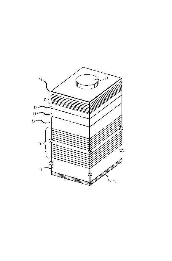
FIG. 1 is a general schematic representation of a VCSEL according to
this invention, denorninated generally as 10. VCSEL 10 comprises a substrate 11; a
quarter-wave stack, 12, of a plurality of pairs of semiconductor layers, one layer of
5 each pair having a refractive index different from the refractive index of another
layer of the pair; a first confining layer, 13; an active layer, 14; a second confining
- layer, 15; a highly-doped contact layer, 16; a metal dot, 17, which acts
simultaneously as a front mirror and as a non-alloyed ohmic top (front) electrode of
the device, and an electrically conductive layer, 18, in contact with the bottom10 surface of substrate 11 forms the bottom (rear) electrode of the device. While not
shown, additional confining and buffer layers may be included into the laser
structure.
Construction of VCSEL 10, in accordance with the invendon, may be
described as being generally as follows:
Substrate 11 is a heavily doped n+-type III-V or II-VI semiconductor,
such as GaAs, GalnAs, InP, InGaPAs, and other related group III-V or II-VI
compound semiconductors. Typically, the thickness of the substrate ranges from
~; 100 to 500 ~m and the doping concentration of the substrate ranges from lxl01~ to
lxlOI9cm~3. In some applications, such as opto-electronic integrated circuitry,
20 substrate 11 may be first grown on a master substrate of silicon, which is in common
~`s to a number of devices grown on the master substrate.
Quarterwave stack 12 is composed of a plurality of pairs (or periods) of
serniconductor layers forming a rear (bottom) multdlayer distributed Bragg reflector
~ (DBR) mirror with a number of pairs typically ranging from 10 to 40. One
; 25 semiconductor layer in each pair has a higher index of refracdon than the other
semiconductor laycr of the pair. The thickness of each semiconductor in the pair~^ equals ~J4, wherein ~ is the opdcal wavelength of the laser device. For a device with
an acdve region lasing at A=0.87~1m, such as a GaAs laser, a quarterwave stack of
~ pairs of such semiconductors as GaAs and AlAs with refractive indices of 3.64 and
- 30 2.97, respecdvely, will consist of 62 nm thick GaAs layer and 73 nm thick AlAs
layer while a stack of AlAs and Alo.0sGao.gsAs will consist of pairs of layers 73 nm
- and 60 nm thick each, respecdvely.
Typically, first confining layer 13 and second confining layer 15 are
s provided to confine active region 14 and to adjust the length (L) of an opdcal cavity
35 (that is, the thickness of the active region). The optical cavity length should be
2I~N-~, wherein N is an integer and ~ is an operating opdcal wavelength of the
.
- s -
laser. Typically, the thickness of each confining layer ranges from 0 to 3 llm. To
obtain constructive interference, the thickness of the confining layers should be a
, multiple of ~/2 or ~/4. In the preferred embodiment the confining regions are of
- Al,~Ga~ As, with x ranging from 0.1 to 0.4.
S Active region 14 is a region in which electrons (-) and holes (+)
recombine providing, under proper stimulation, a lasing emission. In the preferred
embodiment, the active region is a lightly doped (lx10l6 - sx10l7 cm~3) layer ofGaAs with a thickness within a range from 0.1 to lllm. The single layer may be
. replaced by a quantum well (QW) structure composed of a narrow gap
10 semiconductor about l to 30 nm thick, confined by wide-gap semiconductor.
. Alternatively, the single layer forming the acdve region may be replaced by a
superlattice structure which is a multiquantum well structure with very thin barriers.
Highly doped contacting layer 16 is provided in thickness of from 0.01
^~ to 0.1 ~lm to facilitate establishing a non-alloyed ohmic contact between the second
5 confining layer 15 and the mirror/electrode dot 17. Typically7 the doping
concentration in the contacting layer 16 ranges from 1x10l9 to lxlO20cm~3.
Dot 17 is of a metal which acts simultaneously as a front mirror and as a
: front electrode with light emission taking place through the mirror/electrode. In
accordance with this invention, the conductive material is selected from metals, such
20 as Ag and Al, which when deposited in thickness ranging from S nm to 50 nm
exhibit semi-transparent/serni-reflective properties with reflectivity (R) falling within
a range of from 20 to 99 percent and transrnissivity(T) within a range of from 80 to 1
percent. Mirror/electrode 17 is a non-alloyed ohmic contact. Such contacts are
deposited by evaporation at temperatures ranging from 100 to 500C, preferably
25 from 100 to 250C. Higher temperatures could result in undesirable alloying of the
metal into the semiconductor leading to a rough interface morphology which
degrades the reflec~on properties of the metal mirror/electrode.
`~ Metal electrode 18 from 1 to 10 llm thick is formed on the bottom (rear)
surface of substrate 11 to provide for current flow perpendicular through the active
30 region to cause lasing emission. The laser may be mounted with electrode 18 in
contact with a heat-sink plate, e.g. of copper or some other heat-conducdve material
which does not contaminate the materials of the laser.
To increase the efficiency of mirTor perforrnance, a quarter-wave stack,
21, (FIG. 10) from 2 to 20 pairs of high indexllow index material layers similar to
35 the pairs in rear milTor 12, but with p+-type doping (lx10l8 to 5X10l9 cm~3) may be
: interposed between confining layer 15 and highly doped contact layer 16. Stack 21,
~3~
- 6-
is interposed to increase the reflectivity of the top mirror, especially when the
thickness of the metal layer is less than 20 nm.
Semiconductor layers 12 through 16 can be grown upon substrate 11 by
such known methods as metal organic vapor phase epitaxy (MOVPE), also known as
5 metal organic chemical vapor deposidon (MOCVD), or by molecular beam epitaxy
(MBE) or by hydride vapor phase epitaxy (VPE). In the preferred embodiment, the
- ~VCSEL structures are grown by Molecular Beam Epitaxy (MBE) technology in a
Varian Gen II MBE sys~em on heavily doped substrates 11. After layers 12 through16 are grown, the pardally formed structure is transferred to a separate high vacuum
~'10 chamber where a metal layer is deposited as a non-alloyed ohmic contact in a
` ~thickness sufficient to provide desired reflectivity and transparency. Standard
photolithographic techniques are then employed to define circular metal dots 17.Thin rear electrode layer 18, e.g., of In, may then be formed on the bottom surface of
substrate 11. Finally, the rear side of the laser may be mounted via the In electrode
15 or by means of a conductive adhesive, such as epoxy, on a copper slab which serves
as a heat sink in common to other devices.
In the preferred embodiment, the VCSEL is an Al,~Gal_"As/GaAs laser
structure comprising in an ascending sequence 1 to 2 ~m thick In electrode 18, about
500)1m thick (001) oriented heavily doped (2xlOI8cm~3) n+~aAs substrate 11,
20 rear mirror 12 consisdng of a quarter-wave stack of 30 pairs of N+-type
(Sx10l7 - 5x10l8 cm~3) semiconductor layers forming multilayer distributed Braggreflector (DBR) mirror, each pair of the stack consists of a 73 nm thick layer of
n+-AlAs and 60 nm thick layer of AloOsGao.9sAs. The reflectivity spectrum of the: DBR structure (rear mirror 12), as measured with a Perkin-Elmer Lambda 9
. 25 UVIVIS/NIR Spectrophotometer, showed a broad high reflectivity band centered at
-0.87~Lm with a reflectivity > 99 percent, which matches with a calculated
reflectivity cwve very well. The rear mirror is followed by first confinement layer
-13 of n+-AI020Gao80As (SxlOI7cm~3) about 3 llm thick, lightly doped
~`(SxlOI6cm~3) acdve layer 14 of p--GaAs about 0.6 ,um thick, and second
30 confinement layer 15 of p+-AI030Gao7oAs (SxlOI6cm~3) about 0.5 ~m thick. A
thin, heavily doped (5 xlOI9cm~3) contact layer of p+-Alo IOGaO90As, about 0.0625
Jlm thick is deposited on the very top of the layers for ohmic contact purpose. A dot
17 of silver (Ag) about 20 ,um in diameter is formed on top of contact layer 16 in a
thickness from about 5 to 50 nm, preferably 35 nm, under condidons leading to a
35 non-alloyed ohmic contact. In this thickness range silver dot 17 is semi-transparent
to the lasing emission enabling its use as a mirror and as a front electrode of the
:' .
3~
.
- 7 -
.~
VCSEL. Silver is chosen as the metallic mirror/electrode because of its good
conductivity and high reflectivity at wavelengths around 0.87~1m, which corresponds
to the energy band gap of laser active material GaAs.
Transmission Electron Microscopy (TEM) study of the laser structures
S grown in a Varian Gen II molecular beam epitaxy (MBE) system disclosed the
uniformity of the GaAs active region and the interface sharpness of the bottom
~-mirror structure. X-ray 0/20 scans of Ag layers grown in a separate high vacuum
chamber with various thicknesses from 20 to 200 nm deposited at 120C, showed
that the Ag films are polycrystalline. Standard photolithographic techniques were
10 employed to define circular Ag dots 17 with diameters ranging from 5 to 100
micrometers. An etchant of 3HNO3:4H2O was used to etch away the unwanted Ag
regions, which leaves a clean, smooth AIxGa1_xAs surface of contacting layer 16.`~-Lasers were electrically pumped using a fine probe, and the
electroluminescence (EL) spectra were analyzed by a SPEX 1702/04 Spectrometer
15 and a photomultiplier. Current-voltage characterisdcs were checked roudnely with a
SonytTektronix 370 Programmable Curce Tracer. The threshold voltage for the laser
`diode is close to the energy band gap of GaAs gain medium, which is 1.4eV at room
temperature. Above the threshold voltage, the current maintains a linear reladonwith the forward bias, indicating that the nonalloyed Ag contact is ohmic. All the
20 measurements are done at room temperature, and no special cooling techniques are
employed.
EL spectra of the VCSEL with a 20 llm diameter 35 nm thick Ag spot
are shown in FIG. 4. Curve (a) of FIG. 4 is below lasing threshold of 35 mA. Thespectmm is characterized by clear Fabry-Perot (FP) modes. The full width at half25 maximum (FWE~) of the FP modes is 0.74 nm. Curve (b) of FIG. 4 shows the
lasing spectrum above threshold. The width of the lasing peak is less than 0.01 nm
' which is limited by the resolution of the spectrometer. The broad peaks which have
the same peak-t~peak distance (~20.6 nm) as that of the much sharper FP modes are
believed to be due to the spontaneous light emitted from the side of Ag spot. The
30 FWHM of FM modes becomes larger for thinner Ag mirrors. From the finesses of
the FP modes, reflectivities for Ag milrors with different thicknesses are calculated
(seeFIG.5), using known optical constants of Ag, air and AlolGaO.9As. The
.reflectivity of the bottom mirror is chosen to be a unity in the calculations. See
M. Born and E. Wolf, "Principles of Optics," 6th edition, Pergamon Press, New
35 York, 1980, p. 628-631. The reflectivity decreases sharply when the Ag thickness is
less than -40 nm. From the FWHM of the broad peak, a reflectivity of -40 percent
'~
. .
:'
. ~ ,
.... .
. .
~ 3 ~
...
is obtained, which is comparable to the reflectivity between GaAs and air. For 200
nm thick Ag mirrors, only broad peaks are seen, and no sharp FP modes are
observed. The reflectivity at 200 nm Ag thickness shown in FIG. 5 is obtained from
calculation using the optical da~a of Ag. Lasing threshold currents under pulsedS operation versus the thicknesses of Ag mirrors are shown in FIG. 6. The diameter of
the Ag mirrors is 20 ~Lm. The lasing threshold current increases as the Ag minorthickness decreases. This can be qualitatively explained by the declease of the
reflectivities with decreasing Ag thicknesses (see FIG. 5).
FIG. 7 shows the light output from the top Ag minor versus excitation
10 current. The light output is measured with ANDO AQ-1125 optical power meter
~ calibrated around 0.85 llm. The Ag mirror has a diameter of 20 ~m, and is 30 nm
- ~ thick. Injection current pulses with one percent duty cycle (100 ns, 0.1 MHz) were
applied to the laser diode. No power saturation was observed up to the maximum
power of 11.5 mW. Large slope value of 0.76 mW/mA which yields an external
15 differential quantum efficiency of 54 percent at lasing wavelength of 0.86 ~m has
been achieved. Quantum efficiencies for various Ag thicknesses ranging from 23 to
- 100 nm are shown in FIG. 9.
FIG. 8 shows relation between reflection, transrnission and absorption of
Ag minors with Ag thicknesses up to 70 nm. The sum of these parameters always
20 equals 100percent. The three curves shown in FIG.8 are calculated using the
optical constants of Ag, air and AlolGa09As and the reflectivity of bottom (rear)
mirror 12 as unity, see M. Born, et al., supra. Comparison of the absorption and the
transmission curves shows that transmission is gIeater than absorption for
thicknesses < 50 nm. Only such thicknesses are useful for lasing emission through
: 25 the top (fron~) Ag mirror.
, ' '" .