Language selection

Search

Patent 2039783 Summary

Third-party information liability

Some of the information on this Web page has been provided by external sources. The Government of Canada is not responsible for the accuracy, reliability or currency of the information supplied by external sources. Users wishing to rely upon this information should consult directly with the source of the information. Content provided by external sources is not subject to official languages, privacy and accessibility requirements.

Claims and Abstract availability

Any discrepancies in the text and image of the Claims and Abstract are due to differing posting times. Text of the Claims and Abstract are posted:

  • At the time the application is open to public inspection;
  • At the time of issue of the patent (grant).
(12) Patent: (11) CA 2039783
(54) English Title: RASTER SIZE REGULATING CIRCUIT
(54) French Title: CIRCUIT POUR STABILISER LA LARGEUR DE TRAME
Status: Deemed expired
Bibliographic Data
(52) Canadian Patent Classification (CPC):
  • 350/102
(51) International Patent Classification (IPC):
  • H04N 3/23 (2006.01)
  • G09G 1/04 (2006.01)
  • H04N 3/223 (2006.01)
(72) Inventors :
  • LENDARO, JEFFERY BASIL (United States of America)
(73) Owners :
  • THOMSON CONSUMER ELECTRONICS, INC. (United States of America)
(71) Applicants :
(74) Agent: CRAIG WILSON AND COMPANY
(74) Associate agent:
(45) Issued: 1997-01-21
(22) Filed Date: 1991-04-04
(41) Open to Public Inspection: 1991-10-14
Examination requested: 1991-04-04
Availability of licence: N/A
(25) Language of filing: English

Patent Cooperation Treaty (PCT): No

(30) Application Priority Data:
Application No. Country/Territory Date
508,448 United States of America 1990-04-13

Abstracts

English Abstract


An arrangement that compensates for a tendency in a
raster width of a display screen of a video display or television to
increase when a variation in a beam current occurs, decreases an
amplitude of a deflection current to decrease in a nonlinear
manner as a function of an increase in the beam current. At a low
beam current, a given increase in the beam current produces a
decrease in the amplitude of the deflection current that is
substantially greater than caused by the same increase at a high
beam current.


Claims

Note: Claims are shown in the official language in which they were submitted.


7
WHAT IS CLAIMED IS:
1. A raster size regulating apparatus for a video
display, comprising:
means for generating an ultor voltage at an ultor
terminal of a cathode ray tube that produces a beam current such
that an output impedance at said ultor terminal causes said ultor
voltage to change when said beam current changes that tends to
affect a size of a raster on a display screen of said video display;
a deflection circuit output stage responsive to an
output supply voltage for generating a deflection current in a
deflection winding at a controllable amplitude that varies in
accordance with said output supply voltage;
means for generating a first control voltage at a
magnitude that varies in accordance with said beam current; and
a power supply responsive to said first control voltage
for generating said output supply voltage that is coupled to said
output stage to energize said output stage and that varies in
accordance with said first control voltage to decrease said
deflection current amplitude in a nonlinear manner when said
beam current increases so as to regulate said size of said raster,
such that an increase in said beam current by a given amount,
produces a substantially larger decrease in said deflection current
amplitude when said beam current is smaller than a first value
than when said beam current is larger than said first value.

2. An apparatus according to Claim 1 wherein said
ultor voltage generating means comprises, a high voltage
transformer having a first winding for developing in said first
winding first voltage pulses and a high voltage winding for
transformer-coupling said first voltage pulses to said ultor
terminal via a high voltage rectifier.

3. An apparatus according to Claim 2 further
comprising, a resistor coupled in series with said high voltage
winding for generating a beam current indicative voltage in said
resistor that is coupled to said first control voltage generating
means for generating said first control voltage in accordance
therewith.


4. An apparatus according to Claim 2 wherein said
resistor is coupled between a low voltage end terminal of said
high voltage winding and a common conductor.

5. An apparatus according to Claim 1 wherein said
power supply operates as a switch mode power supply.

6. An apparatus according to Claim 5 further
comprising, a delay network that is coupled to said first control
voltage generating means for preventing a sudden increase in said
beam current from producing a distortion in an image on a display
screen of said cathode ray tube.

7. A raster size regulating apparatus for a video
display, comprising:
a high voltage transformer having a first winding for
developing in said first winding first voltage pulses and a high
voltage winding for transformer-coupling said first voltage pulses
to an ultor terminal of a cathode ray tube via a high voltage
rectifier for generating an ultor voltage at said ultor terminal that
produces a beam current such that an output impedance at said
ultor terminal causes said ultor voltage to decrease when said
beam current increases that tends to increase a size of a raster on
a display screen of said video display;
a deflection circuit output stage responsive to a first
control voltage for generating a deflection current in a deflection
winding at a controllable amplitude that varies in accordance with
said first control voltage;
a source of a first current;
a first resistor coupled to said source of said first
current to conduct a first portion of said first current, for
generating said first control voltage in accordance with a voltage
that is developed in said first resistor; and
a transistor having a first main current conducting
terminal that is coupled at a junction between said source of said
first current and said first resistor for conducting a second portion
of said first current and a control terminal that is responsive to

9

said beam current, said transistor operating as a controllable
current source when said beam current is smaller than a
predetermined first value for decreasing the voltage in said first
resistor when said beam current increases that, in turn, causes
said amplitude of said deflection current to decrease, said
transistor operating as a conductive switch when said beam
current is larger than said first value for preventing an increase
in said beam current above said first value from substantially
affecting said deflection current.

8. An apparatus according to Claim 7 further
comprising a diode coupled in series with said first resistor to
form a first series network, wherein said first transistor, is
coupled in parallel with said first series network.

9. An apparatus according to Claim 7 further
comprising, a beam current sampling resistor coupled to said
resistor for generating a beam current representative voltage.

10. An apparatus according to Claim 9 further
comprising, an emitter follower having a base electrode that is
coupled to said beam current indicative voltage and an emitter
electrode that is coupled via a second resistor to said control
terminal of said transistor such that when said beam current is
substantially greater than said first value said emitter follower
clamps an emitter voltage to a predetermined level.

11. A raster size regulating apparatus for a video
display, comprising:
a high voltage transformer having a first winding for
developing in said first winding first voltage pulses and a high
voltage winding for transformer-coupling said first voltage pulses
to an ultor terminal of a cathode ray tube via a high voltage
rectifier for generating an ultor voltage at said ultor terminal that
produces a beam current such that an output impedance at said
ultor terminal tends to cause said ultor voltage to decrease when
said beam current changes, thereby affecting a size of a raster on
a display screen of said video display;


a deflection circuit output stage responsive to a first
control voltage for generating a deflection current in a deflection
winding at a controllable amplitude that varies in accordance with
said first control voltage; and
a transistor stage having a control terminal that is
responsive to said beam current for generating said first control
voltage, said transistor stage operating as a controllable current
source when said beam current is within a predetermined range
of values for varying said first control voltage when said beam
current increases in a manner that causes said amplitude of said
deflection current to decrease and as a switch when said beam
current is outside said range of values.

12. An apparatus according to Claim 11 further
comprising, a driver stage for generating a second control voltage
at said control terminal of said transistor that varies in accordance
with said beam current such that when said beam current is
larger than a predetermined value said driver stage operates as a
clamp circuit to prevent a further increase in said beam current
from substantially affecting said first control voltage.

13. An apparatus according to Claim 11 further
comprising, an R-C filter network coupled to said transistor stage
and having a time constant greater than a millisecond that
reduces a rate of change in said first control voltage when a
change in said beam current occurs.

14. An apparatus according to Claim 13 wherein said
R-C filter network comprises a capacitor, that forms a Miller
feedback in said transistor stage.

15. A raster size regulating apparatus for a video
display, comprising:
means for generating an ultor voltage at an ultor
terminal of a cathode ray tube that produces a beam current such
that an output impedance at said ultor terminal causes said ultor
voltage to change when said beam current changes that tends to
affect a size of a raster on a display screen of said video display;

11
a deflection circuit output stage responsive to a first
control voltage for generating a deflection current in a deflection
winding at a controllable amplitude that varies in accordance with
said first control voltage; and
means for generating said first control voltage at a
magnitude that varies in accordance with said beam current to
decrease said deflection current amplitude when said beam
current increases so as to regulate said size of said raster, said
first control voltage generating means including means for
clamping said first control voltage in accordance with a first
voltage to reduce the variation in said first control voltage and in
said deflection current for a given increase in said beam current
when said beam current is within a first range of values such that
the clamping operation is disabled when said beam current is
within a second range of values.

16. An apparatus according to Claim 15 wherein the
clamping operation causes the amount by which said deflection
current decreases to be smaller for a given increase in said beam
current when said beam current increases above a first
predetermined level.

17. An apparatus according to Claim 16 further
comprising, second means coupled to said first control voltage
generating means for clamping said first control voltage in
accordance with a second voltage when said beam current
increases above a second predetermined level that is larger than
said first predetermined level such that the clamping operation of
said second clamping means is disabled when said beam current is
smaller than said second predetermined level.

Description

Note: Descriptions are shown in the official language in which they were submitted.


2~39783
RASTER ST7F REGULATING CIRCUIT

This invention relates to a raster size regulating
circuit.
A typical deflection circuit output stage of a television
receiver or video display monitor includes a trace switch, a
retrace capacitor, an S-shaping capacitor, and a horizontal
deflection winding. During the retrace interval the switch is
opened, forming a resonant retrace circuit that develops a large
amplitude retrace pulse across the deflection winding. The
deflection winding generates a sawtooth shaped current which is
used to deflect the electron beams horizontally across the screen
of a cathode ray tube (CRT). The deflection retrace pulse may be
used in conjunction with an integrated high voltage transformer
(IHVT) to generate the ultor voltage that accelerates the electron
beams to the phosphor screen of the CRT.
The IHVT includes a high voltage winding which may
be segmented into several winding sections. A high voltage diode
is coupled in series with each winding segment. The large
2 0 amplitude retrace pulse voltage applied to the primary winding of
the IHVT, is stepped up by the high voltage winding, and rectified
by the high voltage diodes to develop an ultor voltage of,
illustratively, 24 to 29 kilovolt.
Deflection sensitivity and thus raster size vary as a
function of the ultor voltage. Variations in the ultor voltage
produced by variations in beam current loading may produce
undesirable variations in raster size that distort the picture
displayed on the picture tube screen. An increase in the level of
the beam current, results in a reduction in the ultor voltage that,
3 0 in turn, increases the width of the raster scan. Conversely, a
decrease in the beam current which results in an increase in the
ultor voltage may reduce the effect of the deflection field on the
beam and cause the raster width to decrease.
The IHVT has a typical source impedance of,
3 5 illustratively, 1 megaohm and delivers ultor current of 1 to 2
milliampere, average, depending upon the desired picture power
of the television receiver. As beam current is drawn by the
picture tube anode, the ultor voltage will drop because of the

2039783
_.
IHVT output impedance and because of the relatively low ultor
terminal capacitance formed by the inner and outer conductive
coatings of the picture tube. At a low beam current, a given
change in the beam current will cause a more significant change in
5 the ultor voltage because the IHVT has a higher output impedance
than at a high beam current.
It may be desirable to vary the supply voltage to the
deflection circuit output stage that controls the amplitude of the
deflection current in a nonlinear manner as a function of a
10 variation of the beam current such that, at the low beam current,
a given increase in the beam current produces a larger decrease in
the supply voltage and in the deflection current amplitude than at
the high beam current.
A raster size regulating apparatus, embodying an
15 aspect of the invention for a video display, includes an
arrangement for generating an ultor voltage at an ultor terminal
that produces a beam current. An output impedance at the ultor
terminal causes the ultor voltage to decrease when the beam
current increases that tends to increase a size of a raster on a
2 0 display screen of the video display. A deflection circuit output
stage is responsive to a first control voltage for generating a
deflection current in a deflection winding at a controllable
amplitude that varies in accordance with the first control voltage.
A magnitude of the first control voltage varies in accordance with
2 5 the beam current to decrease the deflection current amplitude
when the beam current increases in a nonlinear manner so as to
regulate the size of the raster. An increase in the beam current
by a given amount, produces a substantially larger decrease in the
deflection current amplitude, when the beam current is smaller
30 than a first value, than when the beam current is larger than the
first value.
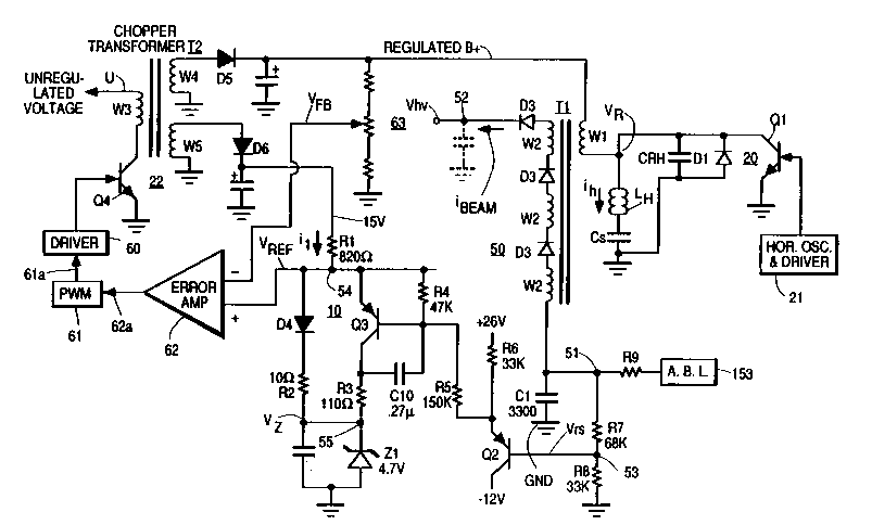
The sole FIGURE illustrates a deflection apparatus with
raster width control, embodying an aspect of the invention.
In the sole FIGURE, a regulated B+ voltage is applied to
3 5 a primary winding W1 of an IHVT, flyback transformer T1.
Primary winding W1 is coupled to a horizontal deflection output
stage 20. Output stage 20 includes a horizontal output transistor
Q1, a deflection damper diode D1, a deflection retrace capacitor

3 20397~3 RCA 85,954

CRH and a horizontal deflection winding LH coupled in a series
relationship with an S-shaping capacitor Cs. A horizontal oscillator
and driver 21 provides the horizontal rate switching of transistor
Q1 to generate a horizontal scanning or deflection current iH in a
5 deflection winding LH and a retrace pulse voltage VR at the
collector of transistor Q 1.
Flyback transformer Tl functions as a high voltage
transformer of a high voltage generator 50. Generator 50
generates an ultor voltage VHV at an ultor terminal 52. To
10 generate ultor voltage VHV , retrace pulse voltage VR is applied to
primary winding Wl, stepped up by a segmented high voltage
winding W2, rectified by corresponding high voltage diodes D3,
and filtered by an ultor capacitance C0 to develop DC ultor voltage
VHV. The ultor capacitance may be provided by the capacitance
15 formed between the inner and outer conductive coatings of the
picture tube, not shown.
A DC current path of a beam current iBEAM supplied
from ultor terminal 52 begins at a ground conductor GND and goes
through resistors R8 and R7 to a resupply terminal 51 of winding
20 W2 that is coupled to the low-AC end of high voltage winding W2.
An automatic beam limiter circuit 153 may be coupled to terminal
51 for limiting video drive to the picture tube when beam current
loading on ultor terminal 52 reaches a predetermined value, in a
well known manner. A filter capacitor Cl is also coupled to
2 5 terminal 51.
A voltage Vrs that is indicative of a magnitude of
beam current iBEAM and that is developed between resistors R7
and R8 is coupled at a beam current sense terminal 53 to a supply
regulator 22, embodying an aspect of the invention, that controls
3 0 the B+ voltage. The B+ voltage regulates the raster size by
decreasing the amplitude of the deflection current as a function of
an increase in the beam current loading, as explained later on.
Supply regulator 22 includes a chopper transistor Q4
that couples an unregulated supply voltage, obtained from, for
3 5 example, a bridge rectifier, not shown, across a winding W3 of a
chopper transformer T2. A diode D5 rectifies a transformer-
coupled voltage developed in a secondary winding W4 of
transformer T2, as a result of a switching operation of transistor

-- 2039783
Q4, for producing B+ voltage. A feedback voltage VFB that is
representative of the B+ voltage is produced at a terminal of a
voltage divider 63 and coupled to an inverting input terminal of
an error amplifier 62. A controllable reference voltage VREF that
5 is produced in a nonlinear network 10, embodying an aspect of
the invention, is coupled to a noninverting input terminal of
amplifier 62. Voltage VREF varies in a nonlinear manner as a
function of the beam current that flows through resistor R8, as
explained later on.
1 0 An output terminal 62a of amplifier 62 is coupled to
an input terminal of a pulse-width-modulator 61 that produces a
pulse-width modulated signal 61 a having a duty cycle that varies
in accordance with the B+ voltage and in accordance with voltage
VREF,controlled by nonlinear network 10. Signal 61a is coupled
1 5 through a driver stage 60 to a base electrode of chopper transistor
Q4 for varying the switching duty cycle of transistor Q4. For a
given level of the beam current or of voltage VREF, the B+ voltage
is maintained constant as a result of the negative feedback loop, in
a well known manner.
2 0 Nonlinear arrangement 10 includes a transistor Q2
having its base electrode coupled to terminal 53 where beam
current representative voltage Vrs is developed. Transistor Q2
operates as an emitter follower having its emitter coupled to a
base electrode of a transistor Q3 via a resistor R5. The emitter
electrode of transistor Q3 is coupled to a terminal 54 for
controlling voltage VREF. The base of transistor Q3 is also coupled
to terminal 53 via a resistor R4. The collector electrode of
transistor Q3 is coupled via a resistor R3 to a cathode of a zener
diode Z1 that develops a zener voltage Vz of 4.7 volts at a
terminal 55. Transistor Q3 and resistor R3 form a variable
impedance or a controllable current source network between
terminals 54 and 55 that varies in response to variations in
voltage Vrs. A diode D4 and a resistor R2, coupled in series, form
a second network that is coupled between terminals 54 and 55 in
3 5 parallel with the variable impedance network of transistor Q3 and
resistor R3.
The base voltage of transistor Q3 is established in
accordance with voltage Vrs and the ratio between resistors R4

2039783
-


and R5. When the beam current is zero, transistor Q3 is
maintained substantially in cut-off as a result of a predetermined
ratio between resistors R4 and R5 forming a voltage divider. A DC
current i 1 through a resistor R 1 that flows to terminal 54 flows
5 substantially through diode D4 and resistor R2 but not through
transistor Q3 when transistor Q3 is in cut-off. Therefore, at zero
beam current, voltage VREF is equal to the sum of zener voltage
Vz, a forward voltage drop in diode D4, VD and a voltage drop
across resistor R2 that is equal to il R2.
As the beam current increases, transistor Q3 conducts
a greater portion of current i1 and, hence, reduces the current flow
through diode D4 and resistor R2. Therefore, voltage VREF
becomes less positive as beam current iBEAM increases. Diode D4
maintains the collector-emitter voltage across transistor Q3 above
its saturation value at a low beam current such that the voltage
across resistor R2 is maintained in the 100-200 mv range.
The increase in beam current iBEAM causes ultor
voltage VHV to decrease as a result of beam current loading of
transformer T1. A decrease in voltage VREF occurs as a result of
the increase in the beam current, as explained before. The
decrease in voltage VREF will cause the B+ voltage to decrease as
well, as a result of the negative feedback loop. The decrease in
the B+ voltage compensates for the tendency of the raster width to
increase as a result of the decrease in ultor voltage VHV.
2 5 At a predetermined level of the beam current,
transistor Q3 becomes fully saturated. Therefore, in accordance
with an inventive feature, a given increase in beam current iBEAM
will have a substantially smaller effect on voltage VREF than at a
lower beam current, when transistor Q3 operates as a controllable
3 0 current source. For example, when the beam current increases
from zero to, for example, 300 ~A, the B+ voltage decreases by
1.3%. In comparison, when the beam current increases from 300
to 1525 ,uA, an increase that is approximately four times than in
the range 0-300 IlA, the B+ voltage decreases by only 0.4%. This
3 5 feature is desirable because at a lower beam current, ultor voltage
V Hv decreases more for a given increase in the beam current
than at a higher beam current. Consequently, in accordance with
an inventive feature, the decrease in the B+ voltage that is

2039783
required for maintaining the raster width constant is made larger
at a low beam current than at a high beam current.
When the beam current is significantly high, transistor
Q2 operates as a clamp to prevent voltage Vrs from becoming
S more negative than -12 volts. Therefore, an undesirable further
decrease in voltage VREF at such significantly high beam current
that would have occurred due to the current increase in resistor
R5 is prevented by the clamping operation.
A capacitor C10 that is coupled between the base and
10 collector of transistor Q3 forms an R-C network with resistors R4
and R5 having a large time constant that is in the milliseconds
range. Such large time constant, advantageously, prevents a fast
change in the beam current due to, for example, television station
channel selection change or a sudden large change in the
15 brightness of the picture scene from producing a fast change in
voltage VREF. Had such fast change in voltage VREF been allowed
to occur, the negative feedback loop that generates voltage B+
might not have been able to respond fast enough. Therefore, a
distortion in the picture and an undesirable sound in transformer
2 0 T2 due to mechanical vibration might have occurred. Thus, the
large value of capacitor C 1 prevents such undesirable transient
condition from occurring.

Representative Drawing
A single figure which represents the drawing illustrating the invention.
Administrative Status

For a clearer understanding of the status of the application/patent presented on this page, the site Disclaimer , as well as the definitions for Patent , Administrative Status , Maintenance Fee  and Payment History  should be consulted.

Administrative Status

Title Date
Forecasted Issue Date 1997-01-21
(22) Filed 1991-04-04
Examination Requested 1991-04-04
(41) Open to Public Inspection 1991-10-14
(45) Issued 1997-01-21
Deemed Expired 2010-04-06

Abandonment History

There is no abandonment history.

Payment History

Fee Type Anniversary Year Due Date Amount Paid Paid Date
Application Fee $0.00 1991-04-04
Registration of a document - section 124 $0.00 1991-09-27
Maintenance Fee - Application - New Act 2 1993-04-05 $100.00 1993-03-04
Maintenance Fee - Application - New Act 3 1994-04-04 $100.00 1994-03-17
Maintenance Fee - Application - New Act 4 1995-04-04 $100.00 1995-03-23
Maintenance Fee - Application - New Act 5 1996-04-04 $150.00 1996-03-21
Maintenance Fee - Patent - New Act 6 1997-04-04 $150.00 1997-03-27
Maintenance Fee - Patent - New Act 7 1998-04-06 $150.00 1998-03-03
Maintenance Fee - Patent - New Act 8 1999-04-05 $150.00 1999-03-01
Maintenance Fee - Patent - New Act 9 2000-04-04 $150.00 1999-12-22
Maintenance Fee - Patent - New Act 10 2001-04-04 $200.00 2001-02-22
Maintenance Fee - Patent - New Act 11 2002-04-04 $200.00 2002-03-08
Maintenance Fee - Patent - New Act 12 2003-04-04 $200.00 2003-03-06
Maintenance Fee - Patent - New Act 13 2004-04-05 $250.00 2004-03-30
Maintenance Fee - Patent - New Act 14 2005-04-04 $250.00 2005-03-07
Maintenance Fee - Patent - New Act 15 2006-04-04 $450.00 2006-03-08
Maintenance Fee - Patent - New Act 16 2007-04-04 $450.00 2007-03-08
Maintenance Fee - Patent - New Act 17 2008-04-04 $450.00 2008-03-07
Owners on Record

Note: Records showing the ownership history in alphabetical order.

Current Owners on Record
THOMSON CONSUMER ELECTRONICS, INC.
Past Owners on Record
LENDARO, JEFFERY BASIL
Past Owners that do not appear in the "Owners on Record" listing will appear in other documentation within the application.
Documents

To view selected files, please enter reCAPTCHA code :


To view images, click a link in the Document Description column. To download the documents, select one or more checkboxes in the first column and then click the "Download Selected in PDF format (Zip Archive)" or the "Download Selected as Single PDF" button.

List of published and non-published patent-specific documents on the CPD .

If you have any difficulty accessing content, you can call the Client Service Centre at 1-866-997-1936 or send them an e-mail at CIPO Client Service Centre.


Document
Description 
Date
(yyyy-mm-dd) 
Number of pages   Size of Image (KB) 
Abstract 1994-02-26 1 13
Claims 1994-02-26 5 210
Drawings 1994-02-26 1 23
Description 1994-02-26 6 281
Cover Page 1994-02-26 1 13
Cover Page 1997-01-21 1 13
Abstract 1997-01-21 1 15
Description 1997-01-21 6 307
Drawings 1997-01-21 1 25
Claims 1997-01-21 5 229
Representative Drawing 1999-07-19 1 22
PCT Correspondence 1996-11-14 1 33
Office Letter 1991-11-22 1 36
Fees 1997-03-27 1 56
Fees 1996-03-21 1 48
Fees 1995-03-23 1 63
Fees 1994-03-17 1 53
Fees 1993-03-04 1 42