Note: Descriptions are shown in the official language in which they were submitted.
2039793
RCA 86,035
- 1 -
APPARATUS FOR CONDITIONING
A SIGNAL PARAMETER
This invention relates to circuitry for controlling the
change of a parameter of a control signal, such as a control signal.
Many systems, such as television receivers, video
cassette recorders, audio signal processors, etc., generate control
signals to condition the systems to operate reliably for input
signals occurring within a range of amplitude or frequency
parameters. An example of such control signals in a television
receiver include automatic gain control (AGC) signals and
automatic chrominance control (ACC) signals. These control
signals are generally generated in a closed loop subsystem
including for example a gain controlling element having an input
terminal for receiving a signal to be controlled and an output
terminal at which parametrically controlled input signal is
available. Control signals are generated by apparatus which is
responsive to the controlled output signal, for measuring a
particular parameter of the signal against a reference value, and
producing, e.g., a difference value for controlling the control
2 0 element.
In many systems it is undesirable for abrupt changes
in control signals to be applied immediately to the signal
controlling element, because abrupt signal changes may produce
adverse affects. For example, abrupt changes in AGC signals may
2 5 produce flicker in a reproduced video image. Therefore, control
signals are frequently coupled to the signal controlling element
via a low pass filter.
Currently many of the aforementioned systems are
being implemented with digital hardware wherein signals are
3 0 processed in binary signal format. (Herein "binary signal" is
intended to mean sampled data signals formed of ones and zeroes
defining numbers representacive of a parameter (e.g., amplitude)
of a signal, and is meant to include binary signals, two's
complement signals, BCD signals, grey code signals, etc.) When
3 5 processing signals in binary format (hereinafter digital format) it
may be inconvenient for various reasons to realize certain
processing functions with circuitry which is a simple digital
analogue of an an;310g circuit. An example is a digital low pass
2~3~793
RCA 86,035
-2-
filter having a long time constant which may require many
sample delay elements, weighting circuits and digital summing
circuits.
The present invention includes circuitry for controlling
a parameter, e.g. the time constant, of a signal. The circuitry
includes means for incrementing or decrementing stored values
that correspond to an output signal having a controlled time
constant. Comparator circuitry, responsive to the output signal
and the input signal, conditions the means for incrementing or
decrementing the stored value to selectively increment or
decrement the stored values at predetermined rates.
Brief Description of the Drawin~s
FIGURES 1 and 2 are block diagrams of alternative
digital signal conditioning circuitry embodying the invention.
FIGURE 3 illustrates waveforms useful for
understanding operation of the invention.
FIGURE 4 is a partially block and partially schematic
diagrams of an analog control signal conditioning circuit
embodying the invention.
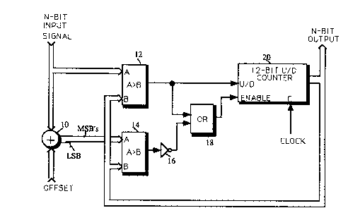
FIGURE 1 illustrates a digital embodiment of apparatus
for conditioning a signal. In FIGURE 1 the "Input Signal" to be
conditioned is assumed to be in N-bit parallel bit format and the
conditioned signal, "Output", is also assumed to be in N-bit parallel
bit format. The output signal is generated by a P-bit up/down
counter 20 (P2N) but only the N most signiffcant bits of the count
values provided by the counter 20 are utilized in the output
signal.
The input signal is applied to one input port, A, of a
comparator 12 and the output signal is coupled to a second input
3 0 port, B, of the comparator 12. Comparator 12 provides a logic one
output signal value whenever the input signal exceeds the output
signal, and provides a logic zero output value otherwise. The logic
levels provided by the comparator 12 are coupled to the up/down
(U/D) control terminal of the counter 20. Logic one and zero U/D
3 5 control values condition the counter 20 to count up and down
respectively.
The input signal is also coupled to a signal summer 10.
An offset number of constant value is applied to a second input of
203~793
RCA 86,035
-3 -
the signal summer 10. Signal summer 10 provides an output
signal which equals the sum of the input signal and the offset
number. Nominally a signal summer arranged to sum N-bit
values has an N+l bit output port. Only the N most significant bits
5 of the output signal provided by the signal summer are utilized.
The offset number is of relatively small value, e.g., 2 to 6.
The output signal provided by the signal summer 10 is
coupled to one input port, A, of a comparator 14, and the output
signal is coupled to a second input port, B. Comparator 14
10 provides a logic one output value whenever the signal provided
by the summer 10 exceeds the output signal, and provides a logic
zero output value otherwise. The output signal provided by
comparator 14 is applied to an inverter 16 wherein the logic
values are inverted (complemented).
The output signals from comparator 1 2 and the
inverter 16 are coupled to respective input terminals of a two-
input OR gate 18. The output signal of the OR gate 18 iS coupled to
an enable terminal of the counter 20. The output signal provided
by the OR gate 18 enables the counter to increment/decrement
2 0 when it is a logic one value and precludes the counter from
incrementing/decrementing when it is a logic zero value.
A clock signal (CLOCK) is applied to a clock input
terminal C of the counter 20, and when counter 20 is enabled,
counter 20 increments/decrements the current count value
25 contained therein by one unit for each clock pulse. Assuming that
counter 20 is a 12-bit counter and that N=7, the N-bit output
signal will increment/decrement at most by one unit every 32
clock pulses. The time constant, i.e., slew rate of the output signal
is determined by the frequency of the clock signal. The frequency
30 of the clock signal is therefore a design choice.
Operation of the circuitry of FIGURE 1 will be
described with reference to the signal waveforms of FIGURE 3.
With respect to FIGURE 3, the input signal, INPUT, and the output
signal, OUTPUT, are drawn in analog form for convenience. The
3 5 assumption is made that the sample rate of the input signal is
much greater than the frequency of the clock signal, CLOCK, which
is applied to the counter. A further assumption is that P is equal
to N, that is, counter 20 is an N-bit counter. Thus the output
203~7~3
RCA 86,035
-4-
signal will increment/decrement for each clock signal when the
counter is enabled. The signal rNPUT is coupled to the A input
port of comparator 12 and the signal INPUT PLUS OFFSET is
coupled to the A input port of comparator 14. The signal OUTPUT
5 is coupled to the respective B input ports of comparators 12 and
14. The waveforms A>B12 and A~B14 are the output signals
provided by comparators 12 and 14 respectively for the given
input signals. The waveform ENABLE is the output signal
provided by the OR gate 18.
At times tl-t4 the counter 20 is enabled and the
output of comparator 12 is high. During this interval the counter
20 is conditioned to increment its count value by one unit per
cycle of the signal clock. It can be seen that the signal OUTPUT
slews positively at a rate which is relatively slow compared to the
slew rate of the signal INPUT.
At times ts-t1o the counter 20 is again enabled,
however during this interval the output of comparator 12 is low,
thus the counter 20 is conditioned to decrement its count value.
The signal OUTPUT decreases by one unit per cycle of the clock
2 0 signal, producing a negative going slew rate which is relatively
long compared to the negatively going slew rate of the signal
INPUT. At all other times illustrated the enable signal is low,
precluding the counter from incrementing or decrementing.
During these times the last count value is stored in the counter.
2 5 The comparator 12 enables the counter to follow
positive going input signal changes and the comparator 14 plus
the inverter 16 enables the counter to follow negative going input
signal changes. The offset value applied to the input signal that is
coupled to comparator 14 is incorporated to preclude the system
3 0 from alternately incrementing and decrementing by one unit
when the input signal is at a relatively constant value, for
example between times t4 and ts.
As illustrated in FIGURES 1 and 3 the positive and
negative going sle~,v rates of the signal OUTPUT are equal. They
may be made unequal by selectively applying clock signals of
different frequencies to the counter 20 during incrementing and
decrementing intervals. The output signal from comparator 12
2039793
RCA 86,035
S
may be utilized to select between two clock signals that are to be
applied to the counter.
As illustrated in FIGURE 3 the output signal was
incremented/decremented by one unit for each clock cycle
5 because P was assumed to be equal to N. Alternatively is P is
greater than N by Q bits, the output signal will be
incremented/decremented by one unit for every 2Q clock cycles.
The apparatus shown in FIGURE 2 is similar to the
apparatus shown in FIGURE 1 with the exception that the signal
10 offset is applied to the output signal coupled to comparator 1 4
rather than to the input signal applied to comparator 14. In
FIGURE 2 the offset value and the output signal are respectively
coupled to the subtrahend and minuend input ports of a
subtracter 400 wherein the constant offset valued is subtracted
15 from the output signal. The output signal minus the offset value
produced by the subtracter are coupled to the B input port of
comparator 14. Operation of the circuit is similar to that
described with respect to the FIGURE 1 circuit.
Regarding both the FIGURE 1 and FIGURE 2 circuits, if
2 0 the dynamic range of the input signal encompasses all possible
values that can be represented by an N-bit signal, it should be
appreciated that the output values of the signal summer 10 and
the subtracter 400 can overflow and underflow. Overflow and
underflow must be prevented or the circuitry will generate
2 5 erroneous results. This may be accomplished by clamping the
output values provided by the summer 10 or subtracter 400 to
values corresponding to the limits of their dynamic range during
intervals when over and/or underflow occur. Such circuitry is
known to those skilled in the art of digital signal processing and
3 0 will not be discussed herein.
FIGURE 4 illustrates an analog embodiment of the
invention. This circuitry may be utilized on an integrated circuit
where it is necessary to provide a relatively long time constant to
a signal. It has the advantage over a simple low pass filter in that
3 5 it utilizes a relatively low valued capacitance which may be
realized in integrated form.
In FIGURE 4, analog input signal is coupled to terminal
200 and the offset value, Vref, is coupled to terminal 201. Output
203~79~
RCA 86,035
-6 -
signal is available from connection 220. Input and output signals
are coupled to respective input terminals of a comparator 208
which corresponds to the comparator 12 in FIGURE 1. Input signal
and the offset value are applied to a node 202 via resistors R1 and
R2. Resistors Rl, R2, R7 and amplifiers 204 and 206 form a
voltage summing network. The resistors R1, R2 and R7 have
equal values, and the amplifier 204 is assumed to have high gain,
thus the output signal provided by the amplifier 206 is equal to
Vinput plus Voffset, where Vinput and Voffset are the amplitude
1 0 values of the input and offset signals. The input signal plus offset
and the output signal are coupled to respective input terminals of
a comparator 210, which corresponds to the comparator 14 in
FIGURE 1. Comparators 208 and 210 provide high level output
signals only when signal applied to their (+) input terminals
1 5 exceeds signal applied to their (-) input terminals, and provide
low level output signals otherwise.
Output signal provided by the comparators 208 and
210 are applied to respective input terminals of an analog OR gate
including emitter coupled transistors 212 and resistor R3. The
output of the OR gate is coupled to control a switch S1, to
selectively pass a signal, Clock, to further switches S2 and S3. The
clock signal, when coupled to switches S2 and S3, closes switches
S2 and S3 when it exhibits a high level pulse and opens switches
S2 and S3 when it exhibits a low level. Resistor R6 coupled
2 5 between the control terminal of switches S2 and S3 and ground
potential, insures that switches S2 and S3 are open in the absence
of clock pulses.
Output signal from comparator 208 is inverted in a
buffer amplifier 214 and coupled to respective signal input
3 0 terminals of the switches S2 and S3. Signal output terminals of
the switches S2 and S3 are respectively coupled to the control
electrodes of a p-type transistor P1 and an n-type transistor N1
connected to operate as gated current sources with respect to
connection 220. An integrating capacitor C 1 is coupled between
3 ~ connection 220 and a point of fixed potential.
Transistor P1 applies charging current to capacitor C1
when its control electrode is biased relatively negatively and is
effectively open circuited when its control electrode is biased
RCA 86,0352 ~ 3 9 7 9 3
-7 -
relatively positively. Transistor Nl applies discharging current to
capacitor C1 when its control electrode is biased relatively
positively and is effectively open circuited when its control
electrode is biased relatively negatively. Resistor R4 coupled
5 between the control electrode of transistor P1 and a positive
supply potential, and resistor R5 coupled between the control
electrode of transistor N1 and ground, insure that transistors P1
and N1 are biased off when switches S2 and S3 are open.
When switch Sl is closed (enabled) by the OR gate the
10 capacitor C1 is selectively charged or discharged depending upon
whether the output of comparator 208 is high or low valued,
respectively. The increments of charge (or discharge) are
dependent upon the width of the clock pulses and the parameters
of transistor P1 (N1). Positive and negative output slew rates will
15 be equal or different depending upon the relative design
parameters selected for transistors P1 and N1.
The output signal at connection 220 will
increment/decrement by a unit of charge for each clock pulse
when switch S1 is closed. This rate of response may be
2 0 lengthened by including an attenuator in the feedback path
between the output (220) and the input terminals of comparators
208 and 210.