Note: Descriptions are shown in the official language in which they were submitted.
;~3~
The present invention relates in general to an
apparatus and method for processing workpieces which
minimizes the use of coating materials, and more
particularly, to an apparatus and method for applying a
layer of a fluid material such as photoresist on the
surface of a semiconductor wafer in a manner to reduce
the consumption of photoresist being used, while at the
same time maintaining or improving uniformity of the
coating during processing of the wafer in the
fabrication of integrated circuits and the like.
In the processing of workpieces such as
semiconductor wafers for the ultimate manufacture of
electronic components, one of the steps required is the
dispensing of a fixed amount of a certain type of fluid
material onto the surface of the wafer. For example, in
the manufacture of integrated circuits, a photoresist
may be dispensed onto a silicon waf~r preliminary to the
photoetching of the wafer. In this regard, there is
known from U.S. Patent No. 4,190,015 an apparatus which
dispenses a fixed amount of a fluid material onto a
semiconductor wafer surface and is then spread evenly
thereon, for example, by spinning the wafer at a high
rate of speed. The fluid material is discharged from a
nozzle in the form of a circular opening formed at the
end of a length of hollow tubing.
U.S. Patent No. 4,551,355 discloses rotating a
disc at high spaed on a spindle while fluid carrying
magnetic medium material is applied to the disc through
a circular dispensing nozzle which starts at the outside
of the disc and travels to the inside diameter, pauses
momentarily, and then travels back to the outside
diameter. As the fluid i5 applied, a thin film of
medium material adheres to the disc while the excess
fluid forms a protective coating over this thin film as
it flows radially off the disc due to the centrifugal
force generated by the high speed rotation. The nozzle
discharge pressure and the high rotational speed of the
disc results in a very thin film of magnetic medium
" ' ' ~ , : ,
~:~39~7~3
--2--
material being applied to the disc. The rate of nozzle
travel can be adjusted to vary the medium material film
thickness.
U.S. Patent No. 3,198,657 discloses a process
for spin coating objects with a pigmented material. The
surface to be spin coated is first wetted by discharging
the material from a cylindrical nozzle onto the spinning
surface from the outer edge to the inner edge of the
surface to be coated. The discharge of the coating
material onto the spinning surface is continued using
conventional spin coating techniques. The discharge of
the coating material may be continued at the inner edge
until an amount of material in excess of the amount
necessary to cover the surface has been dispensed. In
the alternative, the coating material may be continued
at the inner edge only until a wave front of material is
flowing outward over the spinning surface. In this
event, the material is discharged from the inner edge to
the outer edge either by dispensing behind the moving
wave front or by pouring over and in front of the wave
front. At the outer edge of the surface, discharge of
the material is discontinued.
U.S. Patent No. 4,457,259 discloses a spray
apparatus which provides a predetermined, uniform
quantity of liquid such as photoresist de~eloper per
unit area of surface by a parabolic cam mechanism,
arranged to repeatedly reciprocate a circular nozzle at
a predetermined linear velocity a plurality of times
over a spinning semiconductor wafer. The mechanism
moves the nozzle at a parabolic varying velocity such
that the liquid is deposited at a uniform quantity per
unit area. The cam is continuously rotated and engaged
with a cam follower by a programmable timer which
defines the spray period. A similar apparatus which
dispenses the fluid through a circular nozzle in the
form of a continuous spiral bead on a semiconductor
wafer by means of a cam and cam follower arrangement is
known from U.S. Patent No. 4,451,507.
2~39~7~
--3--
U.S. Patent No. 4,267,212 discloses a process
for spin coating a semiconductor wafer uniformly with a
coating solution such as a photographic emulsion by
rotating the wafer at a first speed while simultaneously
applying the coating solution through a circular nozzle
at a radially moving position. Once the semiconductor
wafer has been initially covered, the speed of rotation
of the wafer is increased and rotation continues until a
uniform coating has been obtained. A similar process
having a stationary nozzle is disclosed in U.S. Patent
No. 3,~95,928.
In each of the aforedescribed apparatuses and
methods, the fluid coating material is dispensed in a
column of fluid whose cross-section approximates a
circle, either during wafer rotation or while the wafer
is stationary. Wafer coating is achieved by building up
a pool of the fluid coating material in the nature of a
thick layer and spin casting a film thereof by
accelerating the rotation of the wafer about its own
center in order to remove the excess material and to
leave a thin film coating therebehind. The amount of
fluid coating material, such as photoresist, remaining
on the wafer is known to be a very small fraction of the
amount that is initially dispensed, approximately one
part in one thousand. This results in a substantial
material loss of unusable photoresist along with its
attendant cost. In addition, this creation of a pool of
tha fluid coating material on the wafer surface can
result in the formation of uneven films which might
adversely effect subsequent wafer processing.
Accordingly, there is an unsolved need for an
apparatus and method which minimizes consumption of the
coating material, such as photoresist, during spin
casting and the like, as well as providing a more
uniform thin film coating on semiconductor ~afers during
the fabrication of integrated circuits and other
electronic components therefrom in the semiconductor
industr~. The present invention, therefore, provides an
`
. ~ '
398~
--4--
apparatus and method for applying a thin layer of a
fluid material such as photoresist on the surface of a
wafer which eliminates pooling of the material, which
reduces the amount of the material required for a given
coating thickness, and which enhances uniformity of the
coating thickness.
In accordance with one embodiment of the
present invention, there is described an apparatus for
applying a layer of a fluid material onto the surface of
a wafer, the apparatus constructed of a source of the
fluid material, and a nozzle having a substantially
rectangular shaped opening in communication with the
source through which the fluid material is discharged in
the form of a fluid stream onto the surface of the
wafer.
In accordance with another embodiment of the
present invention, thexe is described an apparatus for
applying a layer of a fluid material onto the surface of
a semiconductor wafer, the apparatus constructed of a
source of the fluid material, supporting means for
supporting the wafer, rotating means for rotating the
wafer about an axis thereof, a nozzle having a
substantially rectangular shaped opening in
communication with the source through which the fluid
material is discharged in the form of a fluid stream
onto the surface of the wafer, and moving means for
moving the nozzle overlying a portion of the surface of
said wafer.
In accordance with another embodiment of the
present invention, there is described a method for
applying a layer of a fluid material onto the surface of
a wafer, the method including supporting a wafer,
supplying fluid material to a nozzle hav.ing a
substantially rectangular shaped opening, moving the
nozzle overlying a portion of the surface of the wafer,
and discharging the fluid material in the form of a
fluid stream through the substantially rectangular
shaped opening onto the surface of the wafer.
;~:03~37~
--5--
In accordance with another embodiment of the present
invention, there is described a method for applying a
layer of photoresist onto the surface of a semiconductor
wafer, the method including supporting a semiconductor
wafer, supplying fluid material to a nozzle having an
opening, moving the nozzle overlying a portion of the
surface of the wafer, and discharging the photoresist in
the form of a narrow elongated substantially rectangular
fluid stream onto the surface of the wafer.
In order that the present invention may be
more fully understood, it will now be described with
reference to the accompanying drawings, in which:
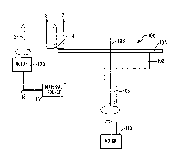
Fig. 1 is a diagrammatic illustration of an
apparatus in accordance with the present invention for
applying a layer of a fluid material such as photoresist
on the surface of a rotating wafer;
Fig. 2 is a cross-sectional view taken along
line 2-2 in Fig. 1 showing the discharge nozzle having
an elongated rectangular or oblong shaped opening;
Fig. 3 is a diagrammatic illustration showing
radial movement of the discharge nozzle during
dispensing of the fluid material onto the surface of the
underlying wafer; and
Fig. 4 is a diagrammatic illustration showing
the path of travel of the major axis of the rectangular
or oblong shaped opening of the discharged nozzle during
dispensing of the fluid material onto the surface of the
wafer.
The present invention provides an apparatus
and method for dispensing a fluid coating material, for
example, a photoresist, onto a spinning surface of a
workpiece in a manner which reduces the consumption of
photoresist used, while at the same time maintaining or
improving uniformity. While the specific embodiment to
be described utilizes photoresist useful in
semiconductor processes in which a planar surface oE a
wafer i5 coated, the present invention can be practiced
using other fluid coating materials useful in coating a
9~
--6--
continuous generally planar surface. Accordingly, the
invention can ~e practiced to provide a coating of a
fluid material in the semiconductor art, optical or
compact disc art and other arts that utilize a spin
coating process for coating fluid material on a
substantially planar surface.
Referring now to the drawings, wherein like
reference numarals in different figures denote like
parts, depicted therein is an apparatus constructed in
accordance with the principles of the present invention
for dispensing a fixed amount of fluid material onto the
surface of a workpiece. The apparatus generally
designated by reference numeral 100 includes a chuck 102
for supporting a workpiece 104, such as a semiconductor
~5 wafer, optical disc, compact disc and the like. The
workpiece 104 is releasably securable to the chuck 102
in a generally horizontal orientation by vacuum created
therebetween as known, for example, from U.S. Patent No.
4,711,610. Howe~er, it is also contemplated that the
workpiece 104 may be held in a generally vertical
orientation by the chuck 102 during the coating process.
The chuck 102 and workpiece 104 are rotatable at high
speeds about axis 106 by means of shaft 108 which is
coupled at one end to a motor 110 or other such device.
The workpiece 104 can be transported to the chuck 102
for processing by a transfer assembly (not shown) as
conventionally known in, for example, the semiconductor
art. One such transfer assembly which includes a
cassette for housing a plurality of workpieces upon
which the fluid material is to be dispensed is known
from U.S. Patent No. 4,190,015.
A hollow tubular dispensing arm 112 is
arranged adjacent the chuck 102 for dispensing the fluid
material through a nozzle 114. The fluid material to be
dispensed is contained within a material source 116
which communicates with the nozzle 114 through the
dispensing arm 112 by means of supply conduit 118. The
dispensing arm 112 is rotated by a motor 120 for
~)3987~
--7--
positioning the nozzle 114 selectively over the surface
o~ the workpiece 104.
As shown in Fig. 2, the nozzle 114 includes a
face portion 122 in which there is provided an elongated
narrow rectangular or oblong shaped opening 124 having a
longitudinal major axis 126 and a transverse minor axis
128. The length of the opening 124 along the major axis
126 is designated by dim~nsion A. The width of the
opening 124 along the minor axis 128 is designated by
dimension B. In illustrating the opening 124 as shown
in Fig. 2, it is to be understood that the opening for
purposes of clarity has been illustrated with dimensions
A and B being greatly exaggerated and not in proper
proportion to each other. In this regard, it is
contemplated that dimension A will be in the range of
from about 0.125 to 0.5 inches, while dimension B will
be in the range of from about 0.001 to 0.02 inches.
However, it is to be understood that these rar.yes for
dimensions A and B are only suggested and that other
values of the respective dimensions A and B outside the
specific ranges disclosed may be utilized in accordance
with the present invention of providing a narrow
rectangular or oblong shaped opening 124. As used
hereinafter, the term substantially rectangular is meant
to include both an elongated narrow rectangular and
oblong shape.
Having no~ described the apparatus 100, the
method of the present invention for applying a layer of
a fluid material on the surface of a workpiece 104 will
be described with specific reference to Figs. 3 and 4.
The workpiece 104 to be processed, such as a
semiconductor wafer, is secured to the chuck 102. When
it is desired to dispense the fluid material, the
dispensing nozzle 114 is initiall~ positioned overlying
the peripheral edge of the workpiece 104. A valve (not
shown) in the supply conduit 118 is opened for a set
period of time to allow the fluid material from the
material source 116 to be dispensed through nozzle 114
37~
--8--
via dispensing arm 112 in the form of a non-aerated
fluid stream. During this set period of time, the
dispensing nozzle 114 is moved along a generally radial
path 130 beginning at the peripheral edge of the
workpiece 104 and terminating at its center. The nozzle
104 is noved along the radial path 130 by rotation of
the dispensing arm 112 by means of motor 120. At the
termination of the set period of time, the valve is
closed, and simultaneously therewith, the nozzle 114 may
be moved to its initial position as shown in Fig. 1.
During dispensing of the fluid material, the workpiece
104 may be rotated at constant or varying speeds to
achieve a uniform coating of a thin film of the desired
fluid material.
Although the dispensing process has been
described as occurring during movement of the nozzle 114
radially inward of the workpiece 104, it is to be
understood that the dispensing operation may occur
during radial outward movement of the nozzle if desired.
In this regard, the nozzle 114 is initially positioned
at a central location overlying the workpiece 104 prior
to beginning the dispensing operation. Alternatively,
the dispensing operation may be performed during both
the radial inward and radial outward movement of the
nozzle 114.
Referring to Fig. 4, the preferred alignment
of the opening 124 with respect to the radial path 130
is shown. In this regard, the major axis 126 of the
opening 12~ follows along in alignment with the radial
path 130. This results in the painting of a broad swath
of the fluid material on the rotating workpiece 104. At
the point o~ contact of the dispensed fluid material
with the surface of the workpiece 104, the fluid stream
has a generally rectangular or oblong cross-section. It
is this general~y narrow elongated rectangular or oblong
shape of the dispensed stream of fluid material which
enables the formation of a uniform coating on the
workpiece 104 with a minimum loss of the fluid material.
3~87~3
g
Surface tension of the fluid material will
ultimately effect the cross-sectional ~hape of the
material subsequent to its discharge through the
rectangular or oblong shaped opening 124~ In this
regard, surface tension will have the tendency to cause
the discharge fluid stream to ultimately assume a
circular shape at a location downstream from the opening
124. The nozzle 124 is therefore positioned a distance
overlying the surface of the workpiece 104 where the
cross-sectional shape of the dispensed fluid stream has
retained substantially its narrow elongated rectangular
or oblong shape. The distance between the surface of
the workpiece 104 and the nozzle 114 required to
maintain this shape of the fluid stream depends upon
many factors. These factors include the viscosity of
the fluid material being discharged, the temperature of
the fluid material, the pressure of the fluid material
at the point of discharge through the opening 124, and
dimensions A and B of the opening. In the semiconductor
art where the fluid material is a photoresist, the
nozzle 114 will be located just off the surface of the
semiconductor wafer, for example, in the range of about
0.005 to 0.50 inches. However, it is to be appreciated
that this distance may be determined through trial and
error as to the shape of the discharged stream of fluid
material at the point of contact with the surface of the
workpiece 104.
: .
.