Note: Descriptions are shown in the official language in which they were submitted.
2 ~ 2 ~ ~
RCA 85,953
,~ VOLTAGE REGllLATQR WITH Cl`IVE TURNOFF
The present invention is directed to a voltage
regulator circuit with an active turnoff capability. In particular,
5 the present invention is direcLed to a circuit configuration in a
signal processing portion of a television receiver in which voltage
regulation is necessary to supply sufficient power to circuit
elements with tight voltage tolerances and where it is important
to maintain a voltage to a control unit while in a standby mode of
10 operation.
It is known to provide a television receiver which is
capable of opera~ion in a plurality of modes. Among the known
modes are an OFF mode, a standby mode, and a normal mode. In
the normal mode, the television receiver operates to process video
15 and audio signals and display and amplify those signals. In this
mode, the signal processing and other functions can be controlled
by various control Gircuit elements including a microprocessor. In
the standby mode the television is in a ready condition but there
is no video or audio signal processing being performed. In this
2 0 mode, the microprocessor is powered and set for operation but the
receiver does not process any audio or video signals.
In a switch mode power supply, embodying an aspec~
- of the invention, a switch mode power supply regulator acts to
regulate a supply voltage that is referenced to a "cold" ground
25 conductor, at a secondary side of an isolation barrier formed by a
chopper transformer. ~egulation of such supply voltage is
- obtained by sensing a voltage that is developed at the secondary
side, during the normal mode. On the other hand, during the
standby mode, regulation of such voltage is obtained by sensing a
3 0 voltage that is referenced to a "hot" ground conductor, at a
primary side of the isolation barrier formed by the chopper
tran sformer.
There may be, for example, two voltages produced a~
the secondary side of the transformer, during both the normal
3 5 operation and standby mode, a first voltage V1 of approximately
15 volts, and a second voltage B+ of approximately 145 volts.
Voltage B+ is sensed during the normal mode. Voltage V1 tracks
.
~
'' '.
2~2~
RCA 85,953
. 2
the voltage B~ due to the cross coupling of the transformer
secondaries.
In the normal mode, the switch mode regulator is
controlled by a horizontal rate pulse width modulated signal
- S derived from a horizontal deflection rate signal developed at a
secondary winding of a horizontal flyback transformer. In the
standby mode, there is no hori~ontal deflection; consequently, the
switch mode regulator cannot be controlled by the horizontal rate
signal. Instead, the switch mode regulator senses a voltage
developed at a winding of the transformer that is at the primary
side of the transformer.
The selec~ion of either the standby mode or the
normal mode of operation is indicated to a switch mode power
supply control circuit, that is at the primary side of the regulator,
and that is referred to herein as the switch mode power supply
~ primary circuit of the regulator7 by the absence or presence,
-~ respectively, of the horizontal line pulse width modulated signal.
The modulated signal is coupled from a pulse width modulator
(PWM) which is coupled to the primary circuit via an isolation
2 0 transformer. When horizontal line rate pulses are received by the
primary circuit, this indicates the normal mode of operation. In
the normal mode of operation, the output pulses of the pulse
width modulator are pulses at the horizontal rate with a variable
pulse ~vidth depending on the level of the sensed B+ voltage. The
2 S switch mode regulator primary circuit produces an output signal
controlled in accordance with the duty cycle of the pulse-width
modulated signal to con~ol the state of a chopper transistor
coupled to a primary winding of the transformer, at the prirnary
side. In particular, the output signal that is developed at a control
3 0 terminal of the chopper transistor is determined by the pulse
width of the signal produced by the PWM and received at the
primary circuit input terminal. If the chopper transistor current
exceeds a predetermined value, typically protective circuits that
are provided in the primary circuit causes the shutdown the
3 5 chopper output transistor. In the standby mode, the pulse width
modulated signal is not generated, and the primary circuit detects
~ such condition by the absence of such signal and operates to
- regulate frorn the primary side.
~.
. .
.~ .
2~259l
RCA 85,953
In the standby mode, however, voltage V 1 that is at
the secondary side is only loosely coupled to the primary circuit at
the primary side of the transforrner because of the loose coupling
in the chopper transformer. Therefore, voltage V 1 is not a tightly
5 regulated as in the normal mode. The voltage V1 is utilized as a
low voltage supply for various loads in the circuitry at the
secondary side of the transformer during both the standby and
normal modes. Voltage B~ is utilized to provide power to the
horizontal output circuitry. It is thus coupled to the horizontal
10 flyback transformer, which has secondary windings for producing
other low voltages, that are developed in filter capacitors during
the normal mode but are not developed during the standby mode.
Voltage V 1 is coupled to energize a remote control receiver which
can be operated by a user of the television from a remote location.
l S When the remote control receiver operates to place
the receiver in the standby mode, these low voltages produced by
the flyback transformer, may not decay quickly despite the
absence of horizontal line rate signals from the flyback
transformer because of the charge on the capacitors. Therefore,
2 0 these low voltages will decay over a transition interval defined by
an RC time constant associated with the capacitors and resistive
circui try .
One of such low voltages that is produced by the
flybaclc transformer is coupled to a base of a regulator transistor
25 for developing the base voltage at the required level. The
collector of such transistor is energized by voltage V1 during both
normal and standby mode. A regulated output supply voltage is
developed at the emitter of the regulator transistor that energizes
stages during the normal mode but not during the standby mode.
3 0 Therefore, as long as the low voltage that is produced by the
flyback transformer has not decayed, current will be drawn from
voltage Vl supply, causing heavier loads on the chopper
transformer. I:)ue to the absence of horizontal line rate signals in
the standby mode, the primary regulator circuit regulates from
3 S the primary side of the transformer. Since regulation is not as
- accurate in the standby mode, as in the normal mode, due to the
loose coupling in the chopper transformer, it may be desirable to
remove all unnecessary loads from the voltage V 1 supply in order
2 0 4 0 2 ~ 4 RCA 85,953
not to cause a transient condition in voltage Vl. The transient
condition could adversely affect circuitry such as the control
microprocessor of the remote control receiver.
In accordance with an aspect of the invention, an
S active turnoff of the regulator transistor is provided immediately
after the receiver goes into the standby mode of operation so as to
actively turnoff the load of voltage ~1 supply to provide for
better regulation on the ~ransforrner primary side in the standby
mode due to the immediate reduction of the load current. This
10 reduction in the load current in the standby mode maintains a
safe voltage level to the remote control receiver circuits which
need to remain operational during the standby mode of the
receiver.
A power supply, embodying an aspect of the
` 15 invention, of a video display apparatus includes a source of an
on/off control signal that is indicative when operation in a run or
normal mode is required and when operation in a standby mode
is required. A power supply regulator generates a first supply
voltage at a first supply terminal, during both the standby and the
2 0 run mode. A transistor has a first main current conducting
-~ terminal that is coupled to the first supply voltage and a second
main current conducting terminal that is coupled to a load circuit.
A deflection circuit output stage responsive to the on/off control
~` signal ~ generates a second voltage, during the run mode, and
2 5 during a transition interva~ that follows the run mode operation.
A third voltage is generated at the control terminal of the
transistor at a first magnitude, in accordance with second voltage,
du~ing the run mode, to enable the transistor to produce a load
current, and at a second magnitude, during the transition interval,
3 0 for actively disabling the transistor during the transition interval.
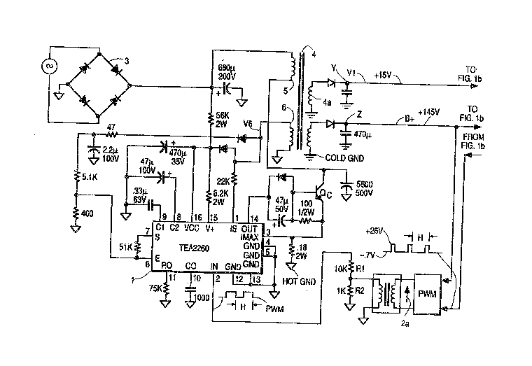
FIGURE l(a) illustrates a first portion of a television
receiver power supply circuit coupled to a load circuit of the
receiver in accordance with an embodiment of the present
-~ invention.
~ 3 5 FIGURE l(b) illustrates the load or secondary circuit of
:~ a television receiver utilizing an embodiment of the present
. .
Invention.
2 0 4 0 2 ~ 4 RCA 85,953
S
FIGURE 1 (a) illustrates a power supply of a television
receiver. The receiver circuitry includes a conventional rectifier
bridge 3 supplying DC power to a primary 5 of a chopper
transformer 4. The primary 5 of the transformer is coupled to a
main chopper transistor QC that is controlled by an output signal
of a control circuit, referred to herein as a primary circuit 1, to
form a switch mode regulator. A winding 6 of the transformer 4
that is referenced to a "hot" ground provides a sensing voltage V6
for primary side regulation in a standby mode of the receiver.
A known primary circuit 1 is a type TEA2260 made
by SGS Thomson. Pin 2 of the primary circuit 1 is coupled to
receive an output signal 2a of a pulse width modulator (PWM) 2
through an isolation transformer 3 and resistors R 1 and R2.
During run or normal mode, the output of the pulse width
: 15 modulator comprises pulses at the horizontal line rate. When such
pulses are received at pin 2 of primary circuit 1, the primary
circui~ operates in the run or normal mode of operation. In that
mode of operation, a voltage B+ at a terminal z of approximately
145 volts and a voltage Vl at a terminal y of approximately 15
2 0 volts are produced and regulated by sensing voltage B+ at the
- secondary side of transformer 4. The pulse width of the pulses
from the pulse width modulator control the power supply
regulation, i.e. the duty cycle of chopper transistor QC, during the
run mode.
2 5 In the standby mode, when no such pulses are
received at pin 2, the voltage, B+ and V1, are regulated by the
primary circuit 1 from voltage V6 at the primary side . Should a
current drain at terminal z be excessive in standby, the voltage
V1 will not be regulated in the standby mode properly as in the
- 3 0 normal mode, because the primary windings 5 and 6 are only
loosely coupled, via the main transformer 4, to a winding 4a at the
- secondary side of the transformer 4 from which voltage Vl is
developed. The primary circuit 1 then controls or regulates from
the "hot" side or the primary side of transformer 4 by sensing the
3 5 voltage at winding 6.
In the normal mode of operation, PWM 2 senses the
145V B+ supply in order to regulate the B~ and +V1 supplies. The
PWM 2 also receives a horizontal line rate signal produced by a
2 0 4 0 2 5 4 RCA 85,953
: 6
secondary 15 of the horizontal output transformer. These
horizontal line rate pulses are switchably processed, typically by
an integration network. to produce a ramp voltage which is used
for generating the pulse width modulated output pulses of PWM
5 2. The pulse width modulated output pulses of PWM 2 are then
supplied to the primary circuit 1 and then to control chopper
~ransis~or QC in order to regulate the B+ supply and, due to the
close tracking, the V1 supply.
In the standby mode, the horizontal line rate signals
10 from secondary 1 5 are not generated because a horizontal
deflection circuitry 333 is disabled. Instead, the primary circuit
regulates vol~age V1 by sensing voltage V6 at the primary side.
As explained previously, such regulation is not as accurate as the
secondary side regulation, provided by PWM 2. Accordingly, in
15 order to keep the V1 voltage which energizes the remote control
circuitry of the receiver regulated, it is desirable to deactivate or
remove unnecessary loads that are not required for the standby
mode operation from the supply voltage V1, as quickly as possible
after a transition from the normal to the standby mode of circuit
20 1. This includes, for example, all the video and audio processing
circuitry .
Voltage Vl is coupled to a remote control receiver 20
which can include a microprocessor, and is also coupled to a
collector of a power transistor Q2 and to a collector of a power
2 5 transistor Ql. These two latter transistors are coupled at their
- emitters to loads to be driven during the normal mode of
-~- operation of the receiver but not during standby. As described
above, in both the standby mode and the normal mode vol~age V 1
~ is approximately 15 volts.
-~ 3 0 It may be desirable to provide controlled or
regulated voltages to the loads of transistors Ql and Q2
respectively. Furthermore, it may be desirable to provide a
supply of regulated voltage to the remote control processor
though primary side regulation of primary circuit 1, during the
- - 3 5 standby mode, so that the processor operates properly.
In the normal mode of operation, the remote control
receiver provides an ON signal to a Horizontal Oscillator and Driver
30 which supplies horizontal drive pulses to the base of a
21) 4 0 2 ~i 4 RCA 85.953
horizontal deflection output transistor QS. The horizontal
. deflection output transistor Q5 produces horizontal rate pulses insecondary 15, which are coupled to the pulse width modulator.
PWM 2, of Figure l (a) as described above. Furthermore, the
S horizontal output or flyback transformer 24 develops a voltage of
approximately 26 volts at a terminal x of a conductor 25, across a
filter capacitor C3. The 26 volt supply is used to energize a first
television receiver Ioad Ll such as a vertical deflection output
stage, not shown. In addition, the +26 volt supply at terminal x is
10 coupled to the collector of transistor Q3 through a resistor R6. The
junction between the collector of transistor Q3 and resistor R6 is
coupled via a voltage divider network of resistors R3, R4 and R5
to the bases of transistor Q2 and of transistor Q1. As a result, a
voltage that is developed at a first junction terminal between
15 resistors R4 and RS, and a voltage that is developed at a second
junction terrninal between resistors R4 and R3 are applied to the
base of transistor Q1 and to the base of transistor Q2, respectively.
The l S volt supply voltage V 1 from the main chopper transformer
4 is supplied to the collectors of power transistors Q1 and Q2.
2 O When, during normal mode, these transistors Ql and
Q2 are ON, +9V and ~12V regulated voltages developed at the
corresponding emitters of the transistors produce currents that
flow in the respective loads L2 and L3. The emitter voltage ~12V
of trahsistor Q 1 is regulated to approximately 12 volts and the
2 S emitter voltage of transistor Q2 is regulated to approximately 9
volts.
`- The voltage +9V at load L3 is regulated in the
following manner. A zener diode Z1 is coupled to the emitter of
transistor Q2. A resistor R7 is coupled between diode Z1 and the
3 0 base of a feedback amplifier transistor Q3. The collector of
transistor Q3 is coupled to collector load resistor R6 and to the
base of transistor Q1. In the normal mode, the ON signal produced
by the remote control receiver turns ON transistor Q4 thereby
-~ coupling a resistor R8 between the base of transistor Q3 and
3 5 ground. Therefore, in the normal mode, a negative feedback loop
is formed and the emitter voltage of transistor Q2 is regulated to
be at 9 volts. Consequently, the power transis~ors Q1 and Q2
operate normally to regulate the two load voltages supplied to
~ ~ ~0402~4 RCA 85,953
loads L2 and L3. Zener diode Z1 level shifts the emitter voltage of
transistor Q2 so that it regulates in a negative feedback manner to
approximately 9 volts. When the receiver is in the ON or normal
~ mode, the base voltage of transistor Q1 is developed across
-~ ~ S resistors R4 and R3.
In the normal mode, the emitter of transistor voltage
Q2 is regulated to the level:
- VZ1 + VBEQ3 (R7 + R8~/R8
~ n the above formula, the base-emitter voltage of
10 transistor Q3 is referred to as VBEQ3 and the zener vol~age as VZ1.
The emitter of transistor Q2 is regulated to 9 volts
with zener diode Z of VZ1=8.2V. Therefore, the base of Q2 will be
9+VBEQ2. The base-emitter voltage of transistor Q2 is referred to
- as VBEQ2. The current through resistors R4 and K3 is made large
15 compared to the base current in transistor Q2. Therefore, the
voltage at the base of transistor Ql is approximately 9.6(R3 +
- ~ R4)/R3 or approximately 12.7 volts in the embodiment shown.
The emitter voltage of transistor Q 1 is thus regulated to
approximately 12.1 volts. Transistors Ql and Q2 are, illustratively,
2 0 of the same type and are operated at the same temperature.
Therefore, good voltage tracking can be achieved. Thus, the
voltages across loads L2 and L3 are maintained at 12 volts and 9
volts respectively. Zener diode Z1 and resistor R7 provide voltage
regulation of the lower voltage, +9V, which in turn regulates the
2 5 higher voltage, +12V, and provides voltage regulation for the
-- receiver loads powered from the secondary side of ~he
transformer 4.
When the remote control reeeiver indicates a change
- from the normal mode to the standby mode, the remote control
30 receiver generates an OFF or standby signal to the base of
transistor Q4 and to the horizontal oscillator and driYer stage 30.
l'his prevents deflection output transistor Q5 from switching,
thereby preventing the voltages at the flyback secondaries 15 and
16 from being produced. Accordingly, PWM 2 ceases to provide
3 5 PWM signal 2a to primary circuit 1 and the switch mode regulator
regulates from the primary side in aecordance with voltage V6.
As discussed, to maintain adequate regulation of the 15V supply
voltage V1, it may be desirable to disable the current drain by the
:: ,
2 t3 ~ 0 2 ~ 4 RCA 85,953
; 9
; loads L2 and L3 from the voltage V1 supply as quickly as possible
c after the remote control receiver generates the OFF signal, because
loads L2 and L3 are powered by the transformer 4.
These loads can still draw current as long as filter
capacitors C2 and C3, coupled to the base of transistors Q1 and Q2,
that are charged during the normal mode, are still not discharge.
If capacitors C2 and C3 do not discharge rapidly enough they will
~? provide sufficient voltage at the base of transistor Ql and of
transistor Q2 to maintain transistor Q 1 and transistor Q2
conductive. It may be desirable to actively turn off load
transistors Ql and Q2 so that they are turned off as quickly as
possible. As discussed, in the standby mode of operation voltage
V 1 may not be regulated so well because secondary winding 16 at
the secondary side is not as tightly coupled to the primary
winding 6 of the transformer 4, during primary side regulation in
standby. Therefore, if transistors Q 1 and Q2 were to continue to
draw current from winding 4a through line 27 due to a delay in
turnoff of transistors Q 1 and Q2, the voltage level applied to the
remote control receiver 20 that may include a control
2 0 microprocessor, might drop below the minimum required level.
`; Such drop in voltage V1 might occur during a transition interval
immediately after the transition to standby mode in the output
signal of remote receiver 20 and in the primary circuit.
The present invention provides an active turnoff of
2 5 transistors Ql and Q2 which counteracts a possible delay due to a
: slow decay of the 26 volts at point X of line 25, during the
transition interval immediately after the transition to the standby
mode. In particular, when the remote control receiver 20
generates its on/off control signal at the OFF or standby state,
3 0 transistor Q4 is turned off. Therefore, the 15 volt source that is
coupled to the collector of transistor Q4 through resistor R9 drives
transistor Q3 ON such that transistor Q3 is in saturation.
Transistor Q3 in saturation actively drives the base voltage of
each of transistors Ql and Q2 to approximately zero volts. As a
3 5 result, transistors Q1 and Q2 are turned off quickly, thereby,
advantageously, removing loads L 1 and L2 from the 15 volt
supply. The voltage across capacitor C2, which results from
~ . . . . .
21~02~
RCA 8S,953
1 0
charging of the capacitor during the normal mode of operation, is
discharged quickly through the transistor Q3.
: A diode Dl may be coupled between the base of
transistor Q1 and terminal x. Diode D1 is provided between the
5 connection point of the load L1 and the base of Ql and accordingly
capacitor 2. Diode Dl that bypasses resistors R5 and R6 allows
capacitor 2 to be discharged more quickly through load L1 when
the +26 volt voltage decays fast enough.
Accordingly, there has been described a low voltage
10 regulator circuit which is capable of switching a nonessential load
connected thereto out of the circuit in order to conserve power
when the television receiver switched to the standby mode of
operation and regulation is more difficult to achieve.
A regulator circuit has also been described wherein a
: 15 lower voltage supply controls the regulation of a higher voltage
supply
`~:
`.'' l
"'
:
. . .
: