Note: Descriptions are shown in the official language in which they were submitted.
EN9-90-012 1 2040304
DESCRIPTION
COMPOUNDING PREPROCESSOR FOR CACHE
Technical Field
This invention relates to digital computers and
digital data processors and particularly to digital
computers and data processors capable of processing two
or more instructions in parallel.
Backqround of the Invention
The performance of traditional computers which
execute instructions one at a time in a sequential manner
has improved significantly in the past largely due to
improvements in circuit technology. Such one-at-a-time
instruction execution computers are sometimes referred to
as "scalar" computers or processors. As the circuit
technology is pushed to its limits, computer designers
have had to investigate other means to obtain significant
performance improvements.
Recently, so called "super scalar" computers have
been proposed which attempt to increase performance by
executing more than one instruction at a time from a
single instruction stream. Such proposed super scalar
machines typically decide at instruction execution time
if a given number of instructions may be executed in
parallel. Such decision is based on the operation codes
(op codes) of the instructions and on data dependencies
which may exist between adjacent instructions. The op
codes determine the particular hardware components each
of the instructions will utilize and, in general, it is
not possible for two or more instructions to utilize the
same hardware component at the same time nor to execute
an instruction that depends on the results of a previous
instruction (data dependency). These hardware and ldata
dependencies prevent the execution of some instruction
.., ~
EN9-90-012 2040304
combinations in parallel. In this case, the affected
instru~tions are instead executed by themselves in a non-
parallel manner. This, of course, reduces the
performance of a super scalar machine.
Proposed super scalar computers provide some
improvement in performance but also have disadvantages
which it would be desirable to minimize. For one thing,
deciding at instruction execution time which instructions
can be executed in parallel takes a small, but
noticeable, amount of time which cannot be very readily
masked by overlapping it with other normal machine
operations. This disadvantage becomes more pronounced as
the complexity of the instruction set architecture
increases. Another disadvantage is that the decision
making must be repeated all over again each time the same
instructions are to be executed a second or further time.
Summary of Invention
One of the attributes of a Scalable Compound
Instruction Set Machine (SCISM) is: Don't do the
parallel execution decision making at execution time. Do
it at an earlier point in the overall instruction
handling process. For example, do it ahead of the
instruction buffer in those machines which have
instruction buffers or instruction stacks. For another
example, do it ahead of the instruction cache in those
machines which flow the instructions through a cache
unit.
Another attribute of a SCISM machine is to record
the results of the parallel execution decision making so
that such results are available in the event that those
same instructions are used a second or further time.
In one embodiment of the present invention, the
recording of the parallel execution decision making is
accomplished by generating tags which are added to or
inserted into the individual instructions in an
instruction stream. These tags tell whether the
,
o`
-
EN9-90-012 3 2040304
instructions can be executed in parallel or whether they
need to be executed one at a time. This instruction
tagginc, process is sometimes referred to herein as
"compounding". It serves, in effect, to combine two or
more individual instructions into a single compound
instruction for parallel processing purposes.
In a particularly advantageous embodiment of the
present invention, the computer is one which includes a
cache storage mechanism for temporarily storing machine
instructions in their journey from a higher-level storage
unit of the computer to the instruction execution units
of the computer and the compounding or instructing
tagging process is performed intermediate to the higher-
level storage unit and the cache storage mechanism so
that there is stored in the cache storage mechanism both
instructions and compounding tags. As is known, the use
of a well-designed cache storage mechanism, in and of
itself, serves to improve the overall performance of a
computer. And the storing of the compounding tags into
the cache storage mechanism enables the tags to be used
over and over again so long as the instructions in
question remain in the cache storage mechanism. As is
known, instructions frequently remain in a cache long
enough to be used more than once.
For a better understanding of the present invention,
together with other and further advantages and features
thereof, reference is made to the following description
taken in connection Wit]l the accompanying drawings, the
scope of the invention being pointed out in the appended
claims.
Brief Description of the Drawings
Referring to the drawings:
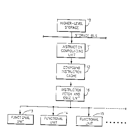
FIG. 1 shows a representative embodiment of a
portion of a digital computer system constructed in
accordance with the present invention;
'3~
,, ~ . . ..
EN9-90-012 4 2040304
FIG. 2 shows a length of an instruction stream
having compounding tags or tag fields associated with the
instructions;
FIG. 3 shows in greater detail the internal
construction of a representative embodiment of an
instruction compounding unit which can be used in the
computer system of Fig. l;
FIG. 4 shows in greater detail a representative
internal construction for each of the compound analyzer
units of Fig. 3;
FIG. 5 shows
an example of logic circuitry that may be used to
implement the compound analyzer and tag generator
portions of Fig. 3 which produce the compounding tags for
the first three instructions in the instruction stream;
FIG. 6 is a table used in explaining the operation
of the Fig. 5 example;
FIG. 7 shows a representative embodiment of a
portion of a digital computer system and is used to
explain how the compounded instructions may be processed
in parallel by multiple functional instructions
processing units;
FIG. 8 shows an example of a particular sequence of
instructions which may be processed by the computer
system of Fig. 7; and
FIG. 9 is a table used in explaining the processing
of the Fig. 8 instruction sequence by the computer system
of Fig. 7-
Description of the Fig. 1 Embodiment
-
EN9-90-012 5 2040304
Referring to Fig. 1 of the drawings, there is shown
a representative embodiment of a portion of a digital
computer system or digital data processing system
constructed in accordance with the present invention.
This c~mputer system is capable of processing two or more
instructions in parallel. It includes a first storage
mechanism for storing instructions and data to be
processed. This storage mechanism is identified as
higher-level storage 10. This storage 10 is a larger-
capacity, lower-speed storage mechanism and may be, for
example, a large- capacity system storage unit or the
lower portion of a comprehensive hierarchical storage
system or the like.
The computer system of Fig. 1 also includes an
instruction compounding mechanism for receiving
instructions from the higher-level storage 10 and
associating with these instructions tag fields which
indicate which of these instructions may be processed in
parallel with one another. This instruction compounding
mechanism is represented by instruction compounding unit
11. This instruction compounding unit 11 analyzes the
incoming instructions for determining which ones may be
processed in parallel. Furthermore, instruction
compounding unit 11 produces for these analyzed
instructions tag information or tag fields which indicate
which instructions may be processed in parallel with one
another and which ones may not be processed in parallel
with one another.
The Fig. 1 system further includes a second storage
mechanism coupled to the instruction compounding
mechanism 11 for receiving and storing the analyzed
instructions and their associated tag fields. This
second or further storage mechanism is represented by
compound instruction cache 12. Cache 12 is a smaller-
capacity, higher-speed storage mechanism of the kind
commonly used for improving the performance rate of a
computer system by reducing the frequency of having to
access the lower-speed storage mechanism 10.
' -
~ EN9-90-012 6 2040304
The Fig. 1 system further includes a plurality of
functional instruction processing units which operate in
parallel with one another. These functional instruction
processing units are represented by functional units 13,
14, 15, et cetera. These functional units 13-15 operate
in parallel with one another in a concurrent manner and
each, on its own, is capable of processing one or more
types of machine-level instructions. Examples of
functional units which may be used are: a general purpose
arithmetic and logic unit (ALU), an address generation
type ALU, a data dependency colapsing ALU (per copending
Canadian application Serial No: 2,039,639, filed March 4,
1991), a branch instruction processing unit, a data
shifter unit, a floating-point processing unit, and so
forth. A given computer system may include two or more of
some of these types of functional units. For example, a
given computer system may include two or more general
purpose ALU's. Also, no given computer system need
include each and every one of these different types of
functional units. The particular configuration of
functional units will depend on the nature of the
particular computer system being considered.
The computer system of Fig. 1 also includes an
instruction fetch and issue mechanism coupled to the
compound instruction cache 12 for supplying adjacent
instructions stored therein to different ones of the
functional instruction processing units 13-15 when the
instruction tag fields indicate that they may be
processed in parallel. This mechanism is represented by
3~ instruction fetch and issue unit 16. Fetch and issue
unit 16 fetches instructions from cache 12, examines
their tag fields and operation code (op code) fields and,
based upon such examinations, sends the instructions to
the appropriate ones of the functional units 13-15.
If a desired instruction is resident in the compound
instruction cache 12, the appropriate address is sent to
the cache 12 to fetch therefrom the desired instruction.
This is sometimes referred to as a "cache hit". If the
r
r
~;
EN9-90-012 7 2 0 4 0 3 0 4
requested instruction does not reside in cache 12, then
it must be fetched from the higher-level storage 10 and
brought into cache 12. This is sometimes referred to as
a "cache miss". When a miss occurs, the address of the
requested instruction is sent to the higher level storage
10. In response thereto, storage 10 commences the
transf~r out or read out of a line of instructions which
includes the requested instruction. These instructions
are transferred to the input of the instruction
compounding unit 11, which unit proceeds to analyze these
incoming instructions and generate the appropriate tag
field for each instruction. The tagged instructions are
thereafter supplied to the compound instruction cache 12
and stored therein for subsequent use, if needed, by the
functional units 13, 14 and 15.
The instruction analysis performed in the
instruction compounding unit 11 does require a certain
relatively small amount of time. However, the
instruction compounding analysis is performed only when
an instruction cache miss occurs and is thus relatively
infrequent.
Fig. 2 shows a portion of a stream of compounded or
tagged instructions as they might appear at the output of
the instruction compounding unit 11 of Fig. 1. As is
seen, each instruction (Instr.) has a tag field added to
it by the instruction compounding unit 11. The tagged
instructions, like those shown in Fig. 2, are stored into
the compound instruction cache 12. As needed, the tagged
instructions in caclle 12 are fetched by the instruction
fetch and issue unit 16. As the tagged instructions are
received by fetch and issue unit 16, their tag fields are
examined to determine if they may be processed in
parallel and their operation code (op code) fields are
examined to determine which of the available functional
units is most appropriate for their processing. If the
tag fields indicate that two or more of the instructions
are suitable for processing in parallel, then they are
sent to the appropriate ones of the functional units in
-
EN9-90-012 8 2 0 4 0 3 0 4
accordance with the codings of their op code fields.
Such instructions are then processed concurrently with
one another by their respective functional units.
When an instruction is encountered that is not
suitable for parallel processing, then it is sent to the
appropriate functional unit as determined by its op code
and it is thereupon processed alone and by itself by the
select~d functional unit.
In the most perfect case, where plural instructions
are always being processed in parallel, the instruction
execution rate of the computer system would be N times as
great as for the case where instructions are executed one
at a time, with N being the number of instructions in the
groups which are being processed in parallel.
Description of Fig. 3 Instruction Compoundinq Unit
Fig. 3 shows in greater detail the internal
construction of a representative embodiment of an
instruction compounding unit constructed in accordance
with the present inven-tion. This instruction compounding
unit 20 is suitable for use as the instruction
compounding unit 11 of Fig. 1. The instruction
compounding unit 20 of Fig. 3 is designed for the case
where a maximum of two instructions at a time may be
processed in parallel. In this case, a one-bit tag field
is used. A tag bit value of "one" means that the
instruction is a "first" instruction. A tag bit value of
"zero" means that the instruction is "second" instruction
and may be executed in parallel with the proceeding first
instruction. An instruction having a tag bit value of
one may be executed either by itself or at the same time
and in parallel with the next instruction, depending on
the tag bit value for such next instruction.
Each pairing of an instruction having a tag bit
value of one with a succeeding instruction having a tag
bit value of zero forms a compound instruction for
parallel execution purposes, that is, the instructions in
EN9-90-012 9 2040304
such a pair may be processed in parallel with one
another. When the tag bits for two succeeding
instructions each have a value of one, the first of these
instructions is executed by itself in a nonparallel
manner. In the worst possible case, all of the
instructions in the sequence would have a tag bit value
of one. In this worst case, all of the instructions
would be executed one at a time in a nonparallel manner.
The instruction compounding unit 20 of Fig. 3
includes a plural-instruction instruction register 21 for
receiving a plurality of successive instructions from the
higher-level storage unit lO. Instruction compounding
unit 20 also includes a plurality of rule- based
instruction analyzer mechanisms. Each such instruction
analyzer mechanism analyzes a different pair of side-by-
side instructions in the instruction register 21 and
produces a compoundability signal which indicates whether
or not the two instructions in its pair may be processed
in parallel. In Fig. 3, there are shown a plurality of
compound analyzer units 22-25. Each of these compound
analyzer units 22-25 includes two of the instruction
analyzer mechanisms just mentioned. Thus, each of these
analyzers units 22-25 produces two of the compoundability
signals. For example, the first compound analyzer unit
22 produces a first compoundability signal M01 which
indicates whether or not Instructions 0 and 1 may be
processed in parallel. Compound analyzer unit 22 also
produces a second compoundability signal M12 which
indicates whether or not Instructions 1 and 2 may be
processed in parallel.
In a similar manner, the second compound analyzer
unit 23 produces a first compoundability signal M23 which
indicates whether or not Instructions 2 and 3 may be
processed in parallel and a second compoundability signal
M34 which indicates whether Instructions 3 and 4 may be
processed in parallel. The third compound analyzer 24
produces a first compoundability signal M45 which
A
EN9-90-012 10 2 0 4 0 3 0 4
indicates whether or not Instructions 4 and 5 may be
processed in parallel and a second compoundability signal
M56 which indicates whether or not Instructions 5 and 6
may be processed in parallel. The fourth compound
analyzer 25 produces a first compoundability signal M67
which indicates whether or not Instructions 6 and 7 maybe
processed in parallel and a second compoundability signal
M78 which indicates whether Instructions 7 and 8 may be
processed in parallel.
The instruction compounding unit 20 further includes
a tag generating mechanism 26 responsive to the
compoundability signals appearing at the outputs of the
analyzer units 22-25 for generating the individual tag
fields for the different instructions in the instruction
register 21. These tag fields T0, T1, T2, etc. are
supplied to a tagged instruction register 27, as are the
instructions themselves, the latter being obtained from
the input instruction register 21. In this manner, there
is provided in the compounding unit output register 27 a
tag field T0 for Instruction 0, a tag field T1 for
Instruction 1, etc.
In the present embodiment, each tag field T0, T1,
T2, etc. is comprised of a single binary bit. A tag bit
value of "one" indicates that the immediately following
instruction to which it is attached is a "first"
instruction. A tag bit value of "zero" indicates that
the immediately following instruction is a "second"
instruction. An instruction having a tag bit value of
one followed by an instruction having a tag bit value of
zero indicates that those two instructions may be
executed in parallel with one another. The tagged
instructions in the compounding unit output register 27
are supplied to the input of the compound instruction
cache 12 of Fig. 1 and are stored into such compound
instruction cache 12.
It should be noted that the amount of register
hardware shown in Fig. 3 can be reduced by storing the
compound instructions directly to the compound
ENg-gO-0l2 11 2040304
instruction cache.
Referring now to Fig. 4, there is shown in greater
detail the internal construction used for the compound
analyzer unit 22 of Fig. 3. The other compound analyzer
units 23-25 are of a similar construction. As shown in
Fig. 4, the compound analyzer 22 includes instruction
compatibility logic 30 for examining the op code of
Instruction O and the op code of Instruction 1 and
determining whether these two op codes are compatible for
purposes of execution in parallel. Logic 30 is
constructed in accordance with predetermined rules to
select which pairs of op codes are compatible for
execution in parallel. More particularly, logic 30
includes logic circuitry for implementing rules which
define which types of instructions are compatible for
parallel execution in the particular hardware
configuration used for the computer system being
considered. If the op codes for Instructions 0 and 1 are
compatible, then logic 30 produces at its output a binary
one level signal. If they are not compatible, logic 30
produces a binary zero value on its output line.
Compound analyzer 22 further includes a second
instruction compatibility logic 31 for examining the op
codes of Instructions 1 and 2 and determining whether
they are compatible for parallel execution. Logic 31 is
constructed in the same manner as logic 30 in accordance
with the same predetermined rules used for logic 30 to
select which pairs of op codes are compatible for
execution in parallel for the case of Instructions 1 and
2. Thus, logic 31 includes logic circuitry for
implementing rules which define which types of
instructions are compatible for parallel execution, these
rules being the same as those used in logic 30. If the
op codes for Instructions 1 and 2 are compatible, then
logic 31 produces a binary one level output. Otherwise,
it produces a binary zero level output.
Compound analyzer 22 further includes first register
dependency logic 32 for detecting conflicts in the usage
~t ~ ,
"~
_
EN9-90-012 12 2040304
of the general purpose registers designated by the Rl and
R2 fields of Instructions 0 and 1. These general purpose
registers will be discussed in greater detail
hereinafter. Among other things, dependency logic 32 may
be constructed to detect the occurrence of a data
dependency condition wherein a second instruction
(Instruction 1) needs to use the results obtained by the
performance of the proceeding instruction (Instruction
0). In this case, either the second instruction can be
executed by the dependency collapsing hardware, thus
executing in parallel with the first instruction, or the
executlon of the second instruction must await completion
of the execution of the preceeding instruction and,
hence, cannot be executed in parallel with the preceeding
instruction. (It is noted that a technique for
circumventing some data dependencies of this type will be
discussed hereinafter.) If there are no register
dependencies which prevent execution of Instructions 0
and l in parallel, then the output line of logic 32 is
given a binary value of one. If there is a dependency,
then it is given a binary value of zero.
Compound analyzer 22 further includes second
register dependency logic 33 for detecting conflicts in
the usage of the general purpose registers designated by
the R1 and R2 fields of Instructions 1 and 2. This logic
33 is of the same construction as the previously
discussed logic 32 and produces a binary one level output
if there are no register dependencies or the register
dependencies can be executed by the data dependency
collapsing hardware, and a binary zero level output
otherwise.
The output lines from the instruction compatibility
logic 30 and the register dependency logic 32 are
- connected to the two inputs of an AND circuit 34. The
output line of AND 34 has a binary one value if the two
op codes being considered are compatible and if there are
no register dependencies. This binary one value on the
AND 34 output line indicates that the two instructions
-
EN9-90-012 13 2040304
being considered are compoundable, that is, are
executable in parallel. If, on the other hand, the AND
34 output line has a binary value of zero, then the two
instructions are not compoundable. Thus, there is
produced on the AND 34 output line a first
compoundability signal M01 which indicates whether or not
Instructions 0 and 1 may be processed in parallel. This
M01 signal is supplied to the tag generator 26.
The output lines from the second compatibility logic
31 and the second dependency logic 33 are connected to
the two inputs of AND circuit 35. AND 35 produces on its
output line a second compoundability signal M12 which has
a binary value of one if the two
op codes being considered (op codes for Instructions 1
and 2) are compatible and if there are no register
dependencies for Instructions 1 and 2 or register
dependencies that can be executed by the data dependency
collapsing hardware. Otherwise, the AND 35 output line
has a binary value of zero. The output line from AND 35
runs to a second input of the tag generator 26.
The other compound analyzers 23-25 shown in Fig. 3
are of the same internal construction as shown in Fig.
for the first compound analyzer 22.
Referring now to Fig. 5, there is shown an example
of the logic circuitry that can be used to implement the
compound analyzer 22 and the portion of the tag generator
26 which is used to generate the first three tags, Tag 0,
Tag 1 and Tag 2. For the example of Fig. 5, it is
assumed that there are two categories of instructions
which are designated as category A and category B. The
rules for compounding these categories of instructions
are assumed to be as follows:
(1) A can always compound with A
(2) A can never compound with B
(3) B can never compound with B
-
EN9-90-012 14 2 0 4 0 3 0 4
(4) B can always compound with A
(5) Rule (4) has preference over Rule (1).
Note that these rules are sensitive to the order of
occurrence of the instructions.
It is further assumed that these rules are such that
when they are observed, there will be no problems with
register dependencies because the rules implicitly
indicate that in case there is any interlock, such an
interlock is always executable by the data dependency
collapsing hardware. In other words, it is assumed for
the Fig. 5 example, that the register dependency logics
32 and 33 of Fig. 4 are not needed. In such case, AND
circuits 34 and 35 are also not needed and the output of
logic 30 becomes the M01 signal and the output of logic
31 becomes the M12 signal.
For these assumptions, Fig. 5 shows the internal
logic circuitry that may be used for the instruction
compatibility logic 30 ~nd the instruction compatibility
logic 31 of Fig. 4. With reference to Fig. 5, the
instruction compatibility logic 30 includes decoders 40
and 41, AND circuits 42 and 43 and OR circuit 44. The
second instruction compatibility logic 31 includes
decoders 41 and 45, AND circuits 46 and 47 and OR circuit
48. The middle decoder 41 is shared by both logics 30
and 31.
The first logic 30 examines the op codes OPO and OP1
of Instructions O and 1 to determine their compatibility
for parallel execution purposes. This is done in
accordance with Rules (1)-(4) set forth above. Decoder 40
looks at the op code of the first instruction and if it
is a category A op code, the A output line of decoder 40
is set to the one level. If OPO is a category B op code,
then the B output line of decoder 40 is set to a one
level. If OPO belongs to neither category A nor category
B, then both outputs of decoder 40 are at the binary zero
level. The second decoder 41 does a similar kind of
EN9-90-012 15 2040304
decoding for the second op code OPl.
AND circuit 42 implements Rule (1) above. If OP0 is
a category A op code and OPl is also a category A op
code, then AND 42 produces a one level output.
Otherwise, the output of AND 42 is a binary zero level.
AND 43 implements Rule (4) above. If the first op code
is a category B op code and the second op code is a
category A op code, then AND 43 produces a one level
output. Otherwise, it produces a zero level output. If
either AND 42 or AND 43 produces a one level output, this
drives the output of OR circuit 44 to the one level, in
which case, the compoundability signal MOl has a value of
one. This one value indicates that the first and second
instructions (Instructions 0 and 1) are compatible for
parallel execution purposes.
If any other combination of op code categories is
detected by decoders 40 and 41, then the outputs of AND
42 and AND 43 remain at the zero level and
compoundability signal M01 has the noncompoundability-
indicating value of zero. Thus, the occurrence of the
combinations indicated by Rules (2) and (3) above do not
satisfy AND's 42 and 43 and MOl remains at the zero
level. If there are further catorgories of op codes in
addition to catorgories A and B, their occurrences in the
instruction stream do not activate the outputs of
decoders 40 and 41. Hence, they likewise result in an M01
compoundability signal value of zero.
The second instruction compatibility logic 31
performs a similar type of op code analysis for the
second and third instructions (Instructions 1 and 2). If
the second op code OPl is a category A op code and the
third op code OP2 is a category A opcode, then, per Rule
(1), AND 46 produces a one level output and the second
compoundability signal M12 is driven to the
compoundability-indicating binary one level. If, on the
other hand OPl is a category B opcode and OP2 is a
category A opcode, then, per Rule (4), AND 47 is
activated to produce a binary one level for the second
-
EN9-90-012 16 2 0 4 0 3 0 4
compoundability signal M12. For any op code combinations
other than those set forth in Rules (1) and (4), the M12
signal has a value of zero.
The M01 and M12 compoundability signals are supplied
to the tag generator 26. Fig. 5 shows the logic
circuitry that can be used in tag generator 26 to respond
to the M01 and Ml2 compoundability signals to produce the
desired tag bit values for Tags 0,1 and 2. The table of
Fig. 6 shows the logic which is implemented by the tag
generator 26 for Tags 0,1 and 2. A tag bit value of one
indicates that the associated instruction is a "first"
instruction for parallel execution purposes. A tag bit
value of zero indicates that the associated instruction
is a "second" instruction for parallel execution
purposes. The only instruction pairs which are
compounded and executed in parallel are those for which
the first instruction in the pair has a tag bit value of
one and the second instruction in the pair has a tag bit
value of zero. Any instruction having a tag bit value of
one which is followed by another instruction having a tag
bit value of one is executed by itself in a singular
manner and not in parallel with the following
instruction.
For the case of the first row in Fig. 6, all three
tag bits have a value of one. This means that each of
Instructions 0 and 1 will be executed in a singular,
nonparallel manner. For the second row of Fig. 6,
Instructions 0 and 1 will be executed in parallel since
Tag 0 has the required one value and Tag 1 has the
required zero value. For the third row in Fig. 6,
Instruction 0 will be executed in a singular manner,
while Instructions 1 and 2 will be executed in parallel
with one another. For the fourth row, Instructions 0 and
1 will be executed in parallel with one another.
For those cases where Tag 2 has a binary value of
one, the status of its associated Instruction 2 is
dependent on the binary value for Tag 3. If Tag 3 has a
binary value of zero, then Instructions 2 and 3 can be
EN9-90-012 17 2 040304
executed in parallel. If, on the other hand, Tag 3 has a
binary value of one, then Instruction 2 will be executed
in a singular, nonparallel manner. It is noted that the
logic implemented for the tag generator 26 does not
permit the occurrence of two successive tag bits having
binary values of zero.
An examination of Fig. 6 reveals the logic needed to
be implemented by the portion of tag generator 26 shown
in Fig. 5. As indicated in Fig. 6, Tag O will always
have a binary value of one. This is accomplished by
providing a constant binary value of one to tag generator
output line 50 which constitutes the Tag O output line.
An examination of Eig. 6 further reveals that the bit
value for Tag 1 3 S always the opposite of the bit value
of the MO1 compoundability signal. This result is
accomplished by connecting output line 51 for Tag 1 to
the ou'_put of NOT circuit 52, the input of which is
connected to the MO1 signal line.
The binary level on Tag 2 output line 53 is
determined by an OR circuit 54 and a NOT circuit 55. One
input of OR 54 is connected to the MO1 line. If MOl has
a value of one, then Tag 2 has a value of one. This
takes care of the Tag 2 values in the second and fourth
rows of Fig. 6. The other input of OR 54 is connected by
way of NOT 55 to the M12 signal line. If Ml2 has a
binary value of zero, this value is inverted by NOT 55 to
supply a binary one value to the second input of OR 54.
This causes the Tag 2 OUtpllt line 53 to have a binary one
value. This takes care of the Tag 2 value for row one of
Fig. 6. Note that for the row 3 case, Tag 2 must have a
value of zero. This will occur because, for this case,
MOl will have a value of zero and M12 will have a value
of one which is inverted by NOT 55 to produce a zero at
the second input of OR 54.
Implicit in the logic of Fig. 6 is a prioritization
rule for the row four case where each of MO1 and M12 has
a binary value of one. This row four case can be
produced by an instruction category sequence of BAA. This
''' ; '
EN9-90-012 18 2 0 4 0 3 0 4
could be implemented by a tag sequence of lOl as shown in
Fig. 6 or, alternatively, by a tag sequence of 110. In
the present embodiment, Rule (5) is followed and the lOl
sequence shown in Fig. 6 is chosen. In other words, the
BA pairing is given preference over the AA pairing.
The 1,1 pattern for M01 and M12 can also be produced
by an op code sequence of AAA. In this case, the 101 tag
sequence of Fig. 6 is again selected. This is better
because it provides a one value for Tag 2 and, hence,
potentially enables Instruction 2 to be compounded with
Instruction 3 if Instruction 2 is compatible with
Instruction 3.
Description of the Fig. 7 Embodiment
Referring to Fig. 7, there is shown a detailed
example of how a computer system can be constructed for
using the compounding tags of the present invention to
provide parallel processing of machine-level computer
instructions. The instruction compounding unit 20 used
in Fig. 7 is assumed to be of the type described iIl Fig.
3 and, as such, it adds to each instruction a one-bit tag
field. These tag fields are used to identify which pairs
of instructions may be processed in the parallel. These
tagged instructions are supplied to and stored into the
compound instruction cache 12. Fetch/Issue control unit
60 fetches the tagged instructions from cache 12, as
needed, and arranges for their processing by the
appropriate one or ones of a plurality of functional
instruction processing units 61, 62, 63 and 64.
Fetch/Issue unit 60 examines the tag fields and op code
fields of the fetched instructions. If the tag fields
indicate that two successive instructions may be
processed in parallel, then fetch/issue unit 60 as~igns
them to the appropriate ones of the functional units 61-
64 as determined by their op codes and they are processed
in parallel by the selected functional units. If the tag
fields indicate that a particular instruction is to be
-
EN9-90-012 19 2040304
processed in a singular, nonparallel manner, then
fetch/issue unit 60 assigns it to a particular functional
unit as determined by its op code and it is processed or
executed by itself.
The first functional unit 61 is a branch instruction
processing unit for processing branch type instructions.
The second functional unit 62 is a three input address
generation arithmetic and logic unit (ALU) which is used
to calculate the storage address for instructions which
transfer operands to or from storage. The third
functional unit 63 is a general purpose arithmetic and
logic unit (ALU) which is used for performing
mathematical and logical type operations. The fourth
functional unit 64 in the present example is a data
dependency collapsing ALU. This dependency collapsing ALU
64 is a three-input ALU capable of performing two
arithmetical/logical operations in a single machine
cycle.
T~e computer system embodiment of Fig. 7 also
includes a set of general purpose registers 65 for use in
executing some of the machine-level instructions.
Typically, these general purpose registers 65 are used
for temporarily storing data operands and address
operands or are used as counters or for other data
processing purposes. In a typical computer system,
sixteen (16) such general purpose registers are provided.
In the present embodiment, general purpose registers 65
are assumed to be of the multiport type wherein two or
more registers may be accessed at the same time.
The computer system of Fig. 7 further includes a
high-speed data cache storage mechanism 66 for storing
data operands obtained from the higher-level storage unit
lO. Data in the cache 66 may also be transferred back to
the higher-level storage unit 10. Data cache 66 may be
of a known type and its operation relative to the higher-
level storage 10 may be conducted in a known manner.
Fig. 8 shows an example of a compounded or tagged
instruction sequence which may be processed by the
EN9-90-012 20 2040304
computer system of Fig. 7. The Fig. 8 example is
composed of the following instructions in the following
sequence: Load, Add, Compare, Branch on Condition and
Store. These are identified as instructions I1-I5,
respectively. The tag bits for these instructions are
1,1,0,1 and 0, respectively. Because of the organization
of the machine shown in Fig. 7, the Load instruction is
processed in a singular manner by itself. The Add and
Compare instructions are treated as a compound
instruction and are processed in parallel with one
another. The Branch and Store instructions are also
treated as a compound instruction and are also processed
in parallel with one another.
The table of Fig. 9 gives further information on
each of these Fig. 8 instructions. The R/M column in
Fig. 9 indicates the content of a first field in each
instruction which is typically used to identify the
particular one of general purpose registers 65 which
contains the first operand. An exception is the case of
the Branch on Condition instruction, wherein the R/M
field contains a condition code mask. The R/X column in
Fig. 9 indicates the content of a second field in each
instruction, which field is typically used to identify a
second one of the general purpose registers 65. Such
register may contain the second operand or may contain an
address index value (X). The B column in Fig. 9
indicates the content of a third possible field in each
instruction, which field may identify a particular one of
the general purpose registers 65 which contains a base
3~ address value. A zero in the B column indicates the
absence of a B field or the absence of a corresponding
address component in the B field. The D field of Fig. 9
indicates the content of a further field in each
instruction which, when used for address generation
purposes, includes an address displacement value. A zero
in the D column may also indicate the absence of a
corresponding field in the particular instruction being
considered or, alternatively, an address displacement
EN9-90-012 21 2040304
value of zero.
Considering now the processing of the Load
instruction of Fig. 8, the fetch/issue control unit 60
determines from the tag bits for this Load instruction
and the following Add instruction that the Load
instruction is to be processed i.n a singular manner by
itself. The action to be performed by this Load
instruction is to fetch an operand from storage, in this
- case the data cache 66, and to place such operand into
the R2 general purpose register. The storage address
from which this operand is to be fetched is determined by
adding together the index value in register X, the base
value in register B and the displacement value D. The
fetch/issue control unit 60 assigns this address
generation operation to the address generation ALU 62.
In this case, ALU 62 adds together the address index
value in register X (a value of zero in the present
example), the base address value contained in general
purpose register R7 and the displacement address value (a
value of zero in the present example) contained in the
instruction itself. The resulting calculated storage
address appearing at the output of ALU 62 is supplied to
the address input of data cache 66 to access the desired
operand. This accessed operand is loaded into the R2
general purpose register in register set 65.
Considering now the processing of the Add and
Compare instructions, these instructions are fetched by
the fetch/issue control unit 60. The control unit 60
examines the compounding tags for these two instructions
and notes that they may be executed in parallel. As seen
from Fig. 9, the Compare instruction has an apparent data
dependency on the Add instruction since the Add must be
completed before R3 can be compared. This dependency,
however, can be handled by the data dependency collapsing
ALU 64. Consequently,
these two instructions can be processed in parallel in
the Fig. 7 configuration. In particular, the control unit
60 assigns the processing of the Add instruction to ALU
-
EN9-90-012 22 2040304
63 and assigns the processing of the Compare instruction
to the dependency collapsing ALU 64.
ALU 63 adds the contents of the R2 general purpose
register to the contents of the R3 general purpose
register and places the result of the addition back into
the R3 general purpose register. At the same time, the
dependency collapsing ALU 64 performs the following
mathematical operation:
R3 + R2 - R4
The condition code for the result of this operation is
sent to a condition code register located in branch unit
61. The data dependency is co]lapsed because ALU 64, in
effect, calculates the sum of R3 + R2 and then compares
this sum with R4 to determine the condition code. In
this manner, ALU 64 does not have to wait on the results
from the ALU 63 which is performing the Add instruction.
In this particular case, the numerical results calculated
by the ALU 64 and appearing at the output of ALU 64 is
not supplied back to the general purpose registers 65.
In this case, ALU 64 merely sets the condition code.
- Considering now the processing of the Branch
instruction and the Store instruction shown in Fig. 8,
these instructions are fetched from the compound
instruction cache 12 by the fetch/issue control unit 60.
Control unit 60 determines from the tag bits for these
instructions that they may be processed in parallel with
3~ one another. It further determines from the op codes of
the two instructions that the Branch instruction should
be processed by the branch unit 61 and the Store
instruction should be processed by the address generation
ALU 62. In accordance with this determination, the mask
field M and the displacement field D of the Branch
instruction are supplied to the branch unit 61.
Likewise, the address index value in register X and the
address base value in register B for this Branch
.
EN9-90-012 23 2040304
instruction are obtained from the general purpose
registers 65 and supplied to the branch unit 61. In the
present example, the X value is zero and the base value
is obtained from the R7 general purpose register. The
displacement value D has a hexadecimal value of twenty,
while the mask field M has a mask position value of
eight.
The branch unit 61 commences to calculate the
potential branch address (0 + R7 + 20) and at the same
time compares the condition code obtained from the
previous Compare instruction with the condition code mask
M. If the condition code value is the same as the mask
code value, the necessary branch condition is met and the
branch address calculated by the branch unit 61 is
thereupon loaded into an instruction counter in control
unit 60. This instruction counter controls the fetching
of the instructions from the compound instruction cache
12. If, on the other hand, the condition is not met
(that is, the condition code set by the previous
instruction does not have a value of eight), then no
branch is taken and no branch address is supplied to the
instruction counter in control unit 60.
At the same time that the branch unit 61 is busy
carrying out its processing actions for the Branch
instruction, the address generation ALU 62 is busy doing
the address calculation (0 + R7 + 0) for the Store
instruction. The address calculated by ALU 62 is
supplied to the data cache 66. If no branch is taken by
the branch unit 61, theII the Store instruction operates
to store the operand in the R~ general purpose register
into the data cache 66 at the address calculated by ALU
62. I~, on the other llaIld, the branch condition is met
and the branch is taken, then the contents of the R3
general purpose register is not stored into the data
cache 66.
The foregoing instruction sequence of Fig. 8 is
intended as an example only. The computer system
embodiment of Fig. 7 is equally capable of processing
~ EN9-90-012 24 2040304
various and sundry other instruction sequences. The
example of Fig. 8, however, clearly shows the utility of
the compound instruction tags in determining which pairs
of instructions may be processed in parallel with one
another.
While there have been described what are at present
considered to be preferred embodiments of this invention,
it will be obvious to those skilled in the art that
various changes and modifications may be made therein
without departing from the invention, and it is,
therefore, intended to cover all such changes and
modifications as fall within the true spirit and scope of
the invention.