Note: Descriptions are shown in the official language in which they were submitted.
- 20~0428
1 FJ-8074/PCT
DESCRIPTION
TRANSFORMING ADAPTORS FOR WAVE DIGITAL
FILTER AND BALANCING NETWORK USING SAME
TECHNICAL FIELD
The present invention relates to transforming
adaptors which are comprised of series and parallel
circuits consisting, as constituent elements, of a
plurality of capacitors and a plurality of resistors
and which perform filter operation functions
corresponding to those constituent elements and to a
balancing network using wave digital filters which are
comprised of these transforming adaptors connected in
cascade.
PRIOR ART
It is advantageous to use wave digital filters
when realizing balancing networks required in two-wire
- 20 transmission systems for digital signals. This is
because, compared with a general digital filter as
represented by a cascade connection of an elementary
digital filter section as expressed by a second order
z function at the numerator and denominator, the
correspondence with the balancing network made by
passive elements in the analog domain is good and the
requisite amount of memory may be reduced and,
further, it is easy to obtain a reflected wave at an
input terminal of the circuit, required as the output
of the balancing network.
The method of designing a balancing network of
the digital type using the idea of a wave digital
filter is known, but the present invention proposes an
improvement of the method of construction and an
improvement of the characteristics.
AS explained in more detail later, a wave digital
filter type balancing network has various merits over
,,~,.
2040428
a general digital filter, but suffers from the problem of a
greater amount of filter operations per each basic sampling clock
and therefore the size of the hardware becomes larger.
DISCLOSURE OF THE INVENTION
In accordance with an embodiment of the present invention
there is provided a wave digital filter corresponding to a
plurality of capacitors and a plurality of resistors operatively
connected to the plurality of capacitors. The wave digital
filter comprises individual transforming adaptors having
operational functions connected in cascade, the individual
transforming adaptors corresponding to the resistors connected
in cascade with adjoining transforming adaptors to form combined
transforming adaptors such that the operational functions are
combined. Each transforming adaptor includes a first adder
receiving first and second inputs and producing an output and a
first incoming wave received as the first input. A second adder,
operatively connected to the first adder, receives a second
incoming wave as a first input receiving the output of the first
adder as a second input and producing an output. A f i r s t
multiplier, operatively connected to the second adder, performs
a predetermined multiplication operation on the output from the
second adder and provides an output. A second multiplier,
operatively connected to the first multiplier, performs a
predetermined multiplication operation on the output from the
first multiplier and provides an output. A third adder,
operatively connected to the second multiplier, receives the
output from the second multiplier as a first input and receives
a third incoming wave as a second input and outputs a reflected
wave. A fourth adder, operatively connected to the second
multiplier, receives the output from the second multiplier as a
first input and provides an output. A delay element, operatively
connected to the first and fourth adders, receives the output
from the fourth adder and provides a delayed signal as the second
input of the first adder. A fifth adder, operatively connected
A
2040428
- 2a -
to the delay element and the fourth adder, receives the output
from the delay element as a first input and receives the output
from the first multiplier as a second input and provides a summed
signal as the second input of the fourth adder.
In accordance with another embodiment of the present
invention there is provided a balancing network which
comprises a first combined transforming adaptor corresponding to
a capacitor and a resistor connected in series with a signal
path. The first combined transforming adaptor comprises a first
adder for receiving as a first input an incoming wave at an input
and outputs the incoming wave at a first output and outputs a
signal at a second output. A second adder, operatively connected
to the first adder, receives as a first input the incoming wave
at an input side and receives as a second input a second output
of the first adder and provides an output. A first multiplier,
operatively connected to the second adder, performs a
predetermined multiplication operation on the output of the
second adder and provides an output. A second multiplier,
operatively connected to the first multiplier performs a
predetermined multiplication operation on the output of the first
multiplier. A third adder, operatively connected to the second
multiplier, receives as a first input an output of the second
multiplier and receives as a second output the incoming wave at
the input side, and outputs the reflected wave at an output. A
fourth adder, operatively connected to the first and fourth
adders, receives as an input the output of the fourth adder and
provides an output which becomes the second input of the first
adder. A fifth adder, operatively connected to the delay
element, the first multiplier and the fourth adder, receives as
a first input the output of the delay element, receives as a
second input the output of the first multiplier, and provides an
output to a second input of the fourth adder. A second combined
transforming adaptor, connected in cascade with the first
transforming adaptor corresponds to a capacitor connected in
~`A~
2040428
- 2b -
parallel and a resistor connected in series with the signal path.
The second combined transforming adaptor comprises a sixth adder
which receives as a first input an incoming wave at an input side
and provides an output. A third multiplier, operatively
connected to the sixth adder performs a predetermined
multiplication operation on the output of the sixth adder and
provides an output. A seventh adder, operatively connected to
the third multiplier receives as a first input an output of the
third multiplier and outputs the incoming wave at an output side
as a first output and outputs a second output. A fourth
multiplier, operatively connected to the sixth adder, performs
a predetermined multiplication operation on the second output of
the seventh adder and provides an output. An eighth adder,
operatively connected to the fourth multiplier, receives as a
first input an output of the fourth multiplier and provides an
output. A fifth multiplier, operatively connected to the eighth
adder, performs a predetermined multiplication operation on a
reflected wave at an input side and provides an output to a
second input of the eighth adder. A ninth adder, operatively
connected to the eighth adder, receives as a first input an
output of the eighth adder and receives as a second input an
incoming wave at the input side, and outputs the reflected wave
at the output side. A tenth adder, operatively connected to the
eighth adder, receives as a first input the output of the eighth
adder and provides an output. A delay element operatively
connected to the sixth, seventh and tenth adders, receives as an
input the output of the tenth adder and provides an output to a
second input of the seventh adder, a second input of the sixth
adder, and a second input of the tenth adder. A third combined
transforming adaptor, connected in cascade with the second
combined transforming adaptor, corresponds to a first capacitor
connected in parallel and a second capacitor connected in series
with the signal path. The third combined transforming adaptor
comprises an eleventh adder for receiving an incoming wave as a
2040428
- 2c -
first input and provides an output. A sixth multiplier,
operatively connected to the eleventh adder, performs a
predetermined multiplication operation on the output of the
eleventh adder and providing an output signal. A twelfth adder,
operatively connected to the sixth multiplier, receives as a
first input an output of sixth multiplier and provides an output.
A thirteenth adder, operatively connected to the twelfth adder,
receives as a first input a first output of the twelfth adder and
provides an output. A seventh multiplier, operatively connected
to the thirteenth adder, performs a predetermined multiplication
operation on the output of the thirteenth adder and provides an
output. A fourteenth adder, operatively connected to the seventh
multiplier, receives as a first input the output of the seventh
multiplier and provides an output. A first delay element,
operatively connected to the thirteenth and fourteenth adders,
receives as an input the output of the fourteenth adder and
provides an output to second inputs of the thirteenth and
fourteenth adders. An eighth multiplier, operatively connected
to the thirteenth adder, performs a predetermined multiplication
operation on the output of the thirteenth adder and provides an
output. A fifteenth adder, operatively connected to the eighth
multiplier, receives as a first input the output of the eighth
multiplier and provides an output. A ninth multiplier,
operatively connected to the twelfth and fifteenth adders,
performs a predetermined multiplication operation on the second
output of the twelfth adder and provides an output to a second
input of the fifteenth adder. A sixteenth adder, operatively
connected to the fifteenth adder, receives as a first input the
output of the fifteenth adder and receives as a second input the
incoming wave, and outputting a reflected wave. A seventeenth
adder, operatively connected to the fifteenth adder, receives as
a first input the output of the fifteenth adder and provides an
output. A second delay element, operatively connected to said
~ ~ ;e
~'
~n404 ?8
- 2d -
eleventh, twelfth and seventeenth adders, receives as an input
the output of the seventeenth adder and provides an output to
second inputs of the eleventh adder, twelfth adder, and
seventeenth adder.
In accordance with a further embodiment of the present
invention there is provided a balancing network disposed in a
terminal office connected to subscribers by 2-wire type pair
cables and connected between a transmission side and a reception
side of a transmission line between the terminal office and
another terminal office. The balancing network comprises a first
combined transforming adaptor corresponding to a capacitor and
a resistor connected in series to a signal path. A second
combined transforming adaptor corresponds to a capacitor
connected in parallel and a resistor connected in series to the
signal path. A third combined transforming adaptor corresponds
to a first capacitor connected in parallel and a second capacitor
connected in series to the signal path, each of said first,
second and third transforming adaptors formed of 3-port pair
transforming adaptors, have a plurality of adders and multipliers
connected in a simplified structure, in a cascade connection with
the 3-port pair transforming adaptors corresponding to resistors
having port pairs other than two port pairs used for the cascade
connection removed and combined with adjoining 3-port pair
transforming adaptors corresponding to capacitors.
BRIEF DESCRIPTION OF THE DRAWINGS
The present invention will be explained below with reference
to the appended drawings, wherein:
Fig. 1 is a view for explaining the gist of a balancing
network;
Fig. 2 is a circuit diagram showing a general example of an
analog ladder type balancing network;
Fig. 3 is a constitutional view of a general wave digital
filter type balancing network;
Fig. 4 is a view of the principle of a first wave digital
~A," -
2040428
filter type balancing network according to the present invention;
Fig. 5 is a view of the principle of a second wave digital
filter type balancing network according to the present invention;
5Fig. 6 is a view of a first embodiment of the first wave
digital filter type balancing network;
2040428
Fig. 7 is a circuit diagram of a prototype analog
ladder type balancing network;
Fig. 8 is a view of an embodiment of the second
wave digital filter type balancing network;
S Fig. 9 is a circuit diagram of a prototype analog
ladder type balancing network;
Fig. 10 is an equivalent wiring diagram showing a
general format of a series 3-port pair adaptor;
Fig. 11 is an equivalent wiring diagram showing a
general format of a parallel 3-port pair adaptor;
Fig. 12 is an equivalent wiring diagram showing a
simplified format of a series 3-port pair adaptor;
Fig. 13 is an equivalent wiring diagram showing a
simplified format of a parallel 3-port pair adaptor;
Figs. 14A, 14B, 14C, and 14D are views showing
the procedure for forming a combined transforming
adaptor 41 of the present invention by combining the
transforming adaptors 21 and 22 (first stage) of Fig.
3;
Figs. lSA, 15B, and 15C are views showing the
procedure for forming a combined transforming adaptor
41 of the present invention by combining the
transforming adaptors 23 and 24 (second stage) of Fig.
3; and
Figs. 16A, 16B, and 16C are views showing the
procedures for forming a combined transforming adaptor
41 of the present invention by combining the
transforming adaptors 25 and 26 ( third stage) of Fig.
3.
BEST MODE FOR CARRYING OUT THE INVENTION
Figure 1 is a view for explaining the gist of a
balancing network, in which figure the present
invention is applied to a balancing network (BNW) 11.
A digital signal from another terminal office
(not shown) is input to a digital signal processing
circuit 12 as a signal Rin at the bottom left of the
figure. In the circuit 12, a level setting is achived,
2040428
the frequency characteristics of the cable loss are
equalized, and the like are performed (omitted from
illustration), and the signal is converted to an
analog signal by a D/A converter of a PCM-CODEC
(CODER-DECODER) and is transferred through a hybrid
transformer 14 and 2-wire pair cable 15 to reach a
subscriber termin~ting circuit 16. On the other hand,
a signal from the subscriber is transferred through
the same pair cable 15 to enter the hybrid transformer
14, is converted to a digital signal by an A/D
converter 17 of the PCM-CODEC of the right side in the
figure, is again input to the digital signal
processing circuit (DSP) 12, where it is adjusted in
level and equalized in frequency characteristics of
the cable loss, and is sent out to the other terminal
office as the signal SOUt.
Here, there is no problem if the impedance of the
cable side viewed from the hybrid transformer 14 is
the characteristic impedance Ro of the circuit, but in
general the impedance Z differs according to the type
of the cable and the length, so the signal from the
other terminal office heading to the subscriber is
transferred to the A/D converter 17 through the hybrid
transformer 14. The transfer characteristic H (equal
to the input voltage of the A/D converter 17 when the
output voltage of an amplifier 18 of the output side
of the D/A converter 13 is 1) is given by the
following equation:
H = (Z - Ro)/[4 (Z + Ro)]
For this, at the digital signal processing
circuit 12, the signal from the other terminal office
is transferred through a balancing network 11 having
the same amplitude and phase characteristics as the
above equation so as to produce a pseudo transfer
signal which is subtracted from the signal from the
A/D converter 17. That is, the function of an echo
canceler is performed. A low pass filter (LPF) of Fig.
2040~28
1 is required for creating interpolation data when the
balancing network 11 must be operated with an over
sampling clock. Further, the equalizer (EQL) is for
compensating for in the transfer characteristic
changes depending on the amplitude and phase
characteristics of the low pass filters attached to
the D/A and A/D converters 13 and 17 in addition to H
of the above equation. The balancing network required
in a two-wire type transmission system may be
replaced, in term of an equivalent circuit, with a
serial and parallel type circuit comprised of
resistors and capacitors. Therefore, it is
advantageous to use a wave digital filter having
operational units corresponding to those elements when
realizing the circuit by digital signals. The problem
of wave digital filters, however, is that the amount
of operations is more than double those of
conventional types of digital filters.
In a wave digital filter, as was stated, there is
the merit of good correspondence with a balancing
network comprised of passive elements in the analog
domain, but in a wave digital filter when the upper
limit of the frequency band region for which balancing
is required becomes close to 1/2 of the frequency of
the sampling clock, the correspondence deteriorates.
Therefore, it is necessary to increase the frequency
of the sampling clock of the wave digital filter and
set the upper limit of the signal frequency band
region to, for example, no more than 1/4 of the
frequency of the sampling clock. Viewing this based on
the upper limit frequency of the signal, the frequency
of the sampling clock becomes not 2 times greater but
a higher multiple, so this is referred to as over
sampling. When the frequency of the sampling clock of
the wave digital filter is made the over sampling
clock having the frequency (n-fs) which is n times
higher than the frequency (fs) of the basic sampling
2040428
clock, the amount of the filter operations increases n
fold.
In a wave digital filter and a balancing network
using a wave digital filter in this way, the large
amount of the operations becomes a problem. This
problem may be explained in more detail as below.
Referring again to Fig. 1, in the case of PCM
transmission by a two-wire system between a subscriber
and a terminal office, use is made of the above-
mentioned balancing network (BNW) 11 to reduce the
transfer of the signal from the reception side (Rin) to
the transmission side (SOut) arising due to mismatching
between the pair cable 15 and a terminating impedance.
In this case, as the circuit for the balancing network
11, use is made of a so-called analog ladder type
circuit (CR ladder type circuit) which is usualy equal
to the equivalent circuit of the pair cable including
the terminating impedance.
Figure 2 is a circuit diagram showing a general
example of an analog ladder type balancing network.
For example, in the case of a pair cable often used in
the U.S. etc. with a length of less than 12 kilofeet
(kft), sufficiently good characteristics can be
obtained by using four capacitors and three resistors
as in this analog ladder type balancing network. Here,
C0 and Cx are DC cutoff capacitors in the terminating
impedance and R~ is a resistor in the terminating
impedance. Therefore, if the impedance level of the
circuit in the figure is matched to the impedance
level of the actual line, then C0 = Cx = 2.16 ~F and
R~ becomes 600Q or 900Q. Note that the portions of Rl,
R2, C1, and C2 in the figure are equivalent elements of
the pair cable itself and differ in value depending on
the type and length of the pair cable.
On the actual line, there are two cases as the
terminating resistor being 600Q and 900Q, as mentioned
above, and further there are cases where the DC cutoff
20~0428
capacitor is 2.16 ~F and cases where it is a larger
capacitance (for example, 33 ~F), i.e., considered to
be substantially short-circuit in the signal frequency
band, so a balancing network with a separate cable
portion and terminating circuits at the two ends as
shown in the figure does not require storaging the
values of the elements of the equivalent circuit after
matching of each and every one of the cables, cable
lengths, terminating conditions, etc, which enables a
great reduction of the required capacity of the
memory. The present invention is based on a balancing
network with a separate cable portion and terminating
circuits at the two ends as shown in the figure.
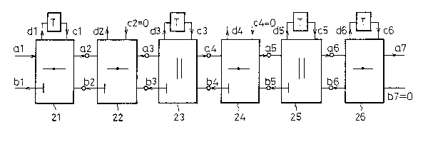
Figure 3 is a constitutional view of a general
wave digital filter type balancing network.
When the circuit of Fig. 2 is transformed to a
wave digital filter, the transforming adaptors 21 to
26 are used to make the transformation for all of the
elements (resistors and capacitors) and the result of
the transformation becomes as shown in the figure. The
transforming adaptors 21 to 26 perform the function of
filter operations. The amount of the operations
becomes as indicated by the "wave filter theory"
described in the latter part of this specification.
Most generally speaking, operations of three
equations, i.e., three multiplication and addition
operations, are required. Therefore, an average of
nine (3 x 3) multiplication and addition operations
and three data storage processing become required per
element, but almost all transforming adaptors are
simplified such that the equation (A-4) stands as in
the later mentioned "wave digital theory", so the
number of multiplication and addition operations
becomes an average eight. In general, when an
operation of a digital filter is performed by a
general purpose digital signal processing LSI (DSP),
one step is normally required for a multiplication and
- 2040~28
addition operation and another one step is required
for storing the data. When the balancing network is of
the circuit construction of Fig. 2, there are six
elements (the final element RX is not counted), so the
total number of steps of operations becomes 11 (8 + 3)
x 6 = 66.
Further, the transmission frequency band region
of signals for usual PCM transmission circuits is 0.3
to 3.4 kHz and the frequency of the basic sampling
clocks is 8 kHz. In this case, the upper limit of the
signal band region is 3.4 kHz and the ratio with the
frequency of the sampling clock is 0.425, close to
0.5, so parameters giving good characteristics for the
wave digital filter cannot be obtained. Therefore, the
frequency of the sampling clock of the wave digital
filter is made 16 kHz, twice the frequency of the
basic sampling clock (already mentioned over
sampling). If doubled in this way, the amount of
operations required per basic sampling clocks doubles,
so the amount of processing of the wave digital filter
type balancing network using the circuit of Fig. 2, as
a prototype circuit, becomes 132 operation steps, a
large amount. Here, "prototype" has the meaning of
"reference". The balancing network using the circuit
of Fig. 2 as a prototype circuit is shown in Fig. 3.
The amount of operations of the wave digital
filter type balancing network required per basic
sampling clock generally becomes a large ll-n (m-1)
and therefore the serious problem arises of an
increase in the size of the hardware, where m denotes
the number of elements and n is (frequency of the
oversampling clock)/(frequency of basic sampling
clock).
The method of designing a wave digital filter is
explained in detail in Alfred Fettweis, Wave Digital
Filters: Theory and Practice", Proceedings of the
IEEE, Vol. 74, No. 2, February 1986, so here the focus
2~0428
will be placed on wave digital filter type balancing
networks using the circuit of Fig. 2 as a prototype
circuit and the method of design and operation of the
same described so as to again clarify the above
problem.
As mentioned above, Fig. 3 shows a wave digital
filter using Fig. 2 as a prototype circuit. In the two
figures, the 3-port pair transforming adaptors shown
by the square blocks are made to correspond with the
elements except for the resistor RX at the right side.
Expl~ining the port pairs using the transforming
adaptor 21 at the left side as an example, al shows
the incoming wave from the left side circuit and bl
the reflected wave going to the left side circuit.
Further, a2 is the reflected wave going to the right
side circuit (the incoming wave for the second
transforming adaptor 22 from the left, so named a2)
and b2 the incoming wave from the right side circuit
(reflected wave for the second adaptor 22, so named
b2). Further, dl is the output wave going to the
element corresponding to the left side transforming
adaptor 21 (in this case C0 of Fig. 2), and cl is the
reflected wave from the element. There are two types
of transforming adaptors (21, 22, 24, and 26 and 23
and 25), one of which corresponds to the series
elements and the other of which corresponds to the
parallel elements. In the case of series elements and
in the case of parallel elements, the relational
equations between the ports differ as explained in the
later mentioned "wave filter theory'.
Here, ak and bk (k is l, 2, 3...) are signals on
physically the same port pair. The signals are
separated into incoming waves (a) and reflected waves
(b) using a relationship similar to the later
mentioned (A-10) as a function of the port impedances
of the port pairs.
The port impedances of the port pairs connected
20~0428
to the elements (resistors R and capacitors C) are set
as follows according to the type of the element:
In the case of a capacitor, T/(2-C)
In the case of a resistor, R (1)
Here, T is the basic sampling period of the wave
digital filter. This T corresponds to the T in Fig. 3
and means, in Fig. 3, a delay for a charging time (T)
of the capacitors.
The port impedances of the port pairs connecting
one transforming adaptor to another transforming
adaptor can be set arbitrarily, but to simplify the
actual filter operations, in a general wave digital
filter, the port impedance RT2 of the right side port
pair in the series 3-port pair transforming adaptors
21, 22, and 24 is set to become the sum of the port
impedance RTl of the left side port pair and the port
impedance RT3 of the top port pair (see RT2 = RT1 + RT3,
shown in the later mentioned equation (A-3)) so that
the later mentioned equation (A-4) stands.
Similarly, in the case of the parallel 3-port
pair transforming adaptors 23 and 25, the port
conductance, which is the inverse of the port
impedance, is set to satisfy the relationship of the
later mentioned equation (A-8).
The port impedance of the left side port pair of
the left side adapter 21 must be made the
characteristic impedance Ro of the hybrid transistor 14
as later explained.
Using the above relationships, if the port
impedances among the transforming adaptors of Fig. 3
are made, from the left, RP1, RP2, RP3~ -- RP5~ the
values of the same become as follows:
RPl = Ro+T/(2-Co) (2)
RP2 = RPl+Rl
RP3 = RPz-[T/Cl/2]/[RPz+T/Cl/2] (4)
RP4 = RP3+Rz ( 5 )
RP5 = RP4 [ T/Cz/ 2]/[ RP4+T/Cz/ 2 ] ( 6 )
2040g28
Using these port impedances, the filter
coefficients y~. of the transforming adaptors become
as follows:
Note that the m in the y~ indicates the three
ports (1, 2, and 3) and the m' in the y~ indicates
the six adaptors (1, 2, 3... 6).
yll = Ro/RPl, y21 = 1, y31 = l-yll (7)
yl2 = RPl/RP2, y22 = 1, y32 = 1-yl2 (8)
yl3 = RP3/RP2, y23 = 1, y33 = 1-yl3 (9)
yl4 = RP3/RP4, y24 = 1, y34 = 1-yl4 (10)
yl5 = RP5/RP4, y25 = 1, y35 = 1-yl5 (11)
yl6 = 2-RPs/RP, y26 = 2-RX/RP, y36 = T/CX/RP (12)
where RP = Rp5+Rx+T/cx/2
On the other hand, the following relationship,
determined by the type of the element, exists for the
incoming wave dm~ to the element and the reflected wave
c~. from the element:
In the case of a capacitor,
c(t) = d(t-T) (where t is the time) (13)
In the case of a resistor
c(t) = 0 (14)
(Note: the resistor elements themselves consume power
and emit heat and do not produce reflected waves.)
If these filter coefficients and relationships
are inserted into the equation of the 3-port pair
transforming adaptors given in the later mentioned
"wave filter theory", the following 15 equations
(equation (15) to equation (29)) stand:
bl(t) = (l-yll)al(t) -yll-b2(t) -yll-dl(t-T) (15)
a2(t) = -al(t) -dl(t-T) (16)
dl(t) = -(l-yll)al(t)-(l-yll)b2(t)
-yll-dl(t-T) (17)
b2(t) = (1-yl2)a2(t) -yl2-b3(t)(18)
a3(t) = -a2(t) (19)
b3(t) = (yl3-l)a3(t) +b4(t) +(1-yrl3)d3(t-T) (20)
a4(t) = yl3- a3(t) +(1-yl3) d3(t-T) (21)
d3(t) = yl3-a3(t) +b4(t) -- yl3-d3(t-T) (22)
- 20~042~
b4(t) = (1-~14)a4(t) - yl4-b5(t) (23)
a5(t) = -a4(t) (24)
b5(t) = (yl5-l)a5(t) +b6(t) +(1-~15)d5(t-T) (25)
a6(t) = yls. a5(t) +(1-~15)d5(t-T) (26)
d5(t) = yl5-a5(t) +b6(t) - -yl5-d5(t-T) (27)
b6(t) = (1-yl6)a6(t) -yl6-d6(t-T) (28)
d6(t) = -y36-a6(t) +(1-y36)d6(t-T) (29)
In the above equation (15) to equation (29), the
relationship of the incoming wave and reflected wave
(above equation (13)) relating to the capacitors, that
is, cl(t) = dl(t-T), c3(t) = d3(t-T), c5(t) = d5(t-T),
c6(t) = d6(t-T), is used to eliminate cm'(t). Further,
the equation of the reflected wave (above equation
(14)) relating to resistors, that is, c2(t) = 0, c4(t)
= 0, b7(t) = 0, is inserted in the equations.
These 15 equations (15) to (29) are recurrence
equations relating to discrete time data. bl(t) at the
time t is calculated as follows: First, the input data
is al(t). dl(t-T), d3(t-T), d5(t-T), and d6(t-T) are
outputs of the top ports of the transforming adaptors
appeared one sampling clock before and are known
values. Therefore, a(3)t is found from the above
equations (16) and (19) and then a5(t) is found from
the equations (21) and (24). Further, a6(t) is
obtained from equation (26). This a6(t) and d6(t-T) is
used to find b6(t) and d6(t) from equations (28) and
(29). d6(t) is used for the calculation at the next
sampling time, that is, t+T. Next, b6(t) and the
already known a5(t) and d5(t-T) are used to calculate
b5(t) and d5(t) from equations (25) and (27).
Next, b4(t) is calculated from equation (23) and
b3(t) and d3(t) are calculated from equations (20) and
(22).
Then, b2(t) is calculated from equation (18) and
bl(t) and dl(t) are calculated from equations (15) and
(17)-
The bl(t) found in this way is the value at the
20~0428
-
13
time t of the reflected wave sought and is calculated
with respect to successive inputs al(t) at the times
t+T, t+2T
Consider the processing using the general purpose
digital signal processing LSI (DSP). In this DSP, in
general the multiplication and addition operation of A
x B + D -> D is processed in one cycle, but processing
of addition alone also requires one cycle. Further,
the load processing of data from the memory can be
performed in parallel with the operation except with
the initial first and second operations, but it is
impossible to perform the processing for storing the
results in the memory in parallel and another
processing cycle than that operation becomes
necessary.
In the processing of the above equations (lS) to
(29), 34 multiplication and addition operations and 15
storage processings are required, for a total of 49
(34+15) cycles. The 49 operation steps per six
elements is smaller than the 66 operation steps
mentioned earlier. This is because if the resistor
elements are included, the special condition of the
reflected wave = 0 (above equation (14)) is added.
If the frequency of the sampling clock of the
balancing network is made n times the frequency of the
basic sampling clock, then 49 cycles become necessary
per one basic sampling clock, which can still be said
to be a large size. Usually, n = 2 is sufficient in a
balancing network of a PCM transmission line, so if n
= 2, the number of cycles necessary for processing of
the balancing network becomes 98 and an average 16
cycles are necessary per element. n is the ratio
mentioned earlier, that is, (the frequency of the
oversampling clock) / (the frequency of the basic
sampling clock). When the usual digital filter is
operated with an oversampling of n = 2, then a second
order, or about 2.5 times the number of cycles, is
- 20~0428
-
14
required compared with just the 12 cycles per two
elements.
As explained in detail above, a wave digital
filter type balancing network has the above-mentioned
merits compared with a general digital filter, but has
the problem of a greater amount of filter operations
per basic sampling clock and therefore the hardware
becomes larger in size.
Figure 4 is a view of the principle of a first
wave digital filter type balancing network according
to the present invention. Among the plurality of
transforming adaptors 31 and 32 (21 to 26 in Fig. 3),
the transforming adaptors 31 (22, 24, 26)
corresponding to the resistors R (R1, Rz, etc.) are
combined with the adjoining transforming adaptors (32
(21, 23, 25) to form a plurality of combined
transforming adaptors 41 and these combined
transforming adaptors 41 are connected in cascade to
form a balancing network.
Note that a and b are the above-mentioned
incoming wave and reflected wave.
Figure 5 is a view of the principle of a second
wave digital filter type balancing network according
to the present invention. In the figure, the wave
digital filter type balancing network is operated by
an oversampling clock (CKn) having a frequency n times
(n being an integer of 2 or more) the basic sampling
clock (CK), a discrete filter output (OUT) is obtained
for each basic sampling clock (CK), and the filter
operations in the basic sampling clocks (CK) are
performed divided into n times by making each of the
plurality of combined transforming adaptors 41 by n
times a number of sectional combined transforming
adaptors 41', 41" and making the values of the filter
coefficients differ among the sectional combined
transforming adaptors 41', 41".
The functions of the above first and second wave
20~0428
digital filter type balancing networks are as follows:
The first wave digital filter type balancing
network (Fig. 4) takes note of the fact that there is
no reflected wave from the resistor elements (R) (see
above-mentioned equation (14)) and eliminates the
ports. Along with elimination of the ports, the
adjoining adaptors are combined to form the single
transforming adaptors 41. This leads to a reduction of
the amount of operations.
The second wave digital filter type balancing
network (Fig. 5) uses the oversampling operation to
enable a plurality of transforming adaptors with
different filter coefficients to be used in one basic
sampling clock (CX). By dividing the filter processing
into a first half and a second half and changing the
filter coefficient, it is fully conceivable that a
balancing network with a higher precision could be
obtained, but if using both the processing results of
the first half and the second half, in general the
operation would be performed as a time variable
filter, so the problem would arise of a different
frequency component is induced. Here, however, only
one of the results, either of the first half or second
half, is used, so this problem does not occur and it
is possible to improve the precision of the balancing
network.
(1) First Wave Digital Filter Type Balancing
Network
Figure 6 is a view of a first embodiment of the
first wave digital filter type balancing network, and
Fig. 7 is a circuit diagram of a prototype analog
ladder type balancing network. The circuit of Fig. 7
is exactly the same as the above-mentioned circuit of
Fig. 2, but the elements forming the transforming
adaptors are at least two elements each as shown by
the dot-chain line (in the past one transforming
adaptor corresponded to one element). Therefore, in
2040428
16
Fig. 6, the number of transforming adaptors is reduced
from the conventional six to three. The first combined
transforming adaptor 41 (ADl) is a combination of the
first and second transforming adaptors 21 and 22
counted from the left in the conventional wave digital
filter (Fig. 3), the second combined transforming
adaptor 41 (AD2) iS a combination of the third and
fourth transforming adaptors 23 and 24 of the
conventional filter, and the third combined
transforming adaptor 41 (AD3) iS a combination of the
fifth and sixth transforming adaptors 25 and 26 of the
conventional filter.
A point in the combination is that a resistor is
connected to one of the ports of one of the adaptors
among the original two transforming adaptors. Even in
the sixth transforming adaptor 26 of the conventional
wave digital filter, the top port is connected to a
capacitor, but a resistor is connected to the right
port. In this case, there are three port pairs for
each new combined transforming adaptor 41. The
relationship among these port pairs differs from the
conventional series adaptor and parallel adaptor, but
the amount of operations does not increase. The
incoming waves al, a3, a5, dl, d3, d5, and d6 and the
reflected waves cl, c3, c5, and c6 are the same as in
the case of Fig. 3.
The relationship among these can be derived by
eliminating a2, b2, a4, b4, a6, and b6 from the
equations (15) to (29). The results are shown by the
following equations:
bl(t) = (l-yll-yl2)al(t) +yll-yl2-b3(t)
- yll-yl2-dl(t-T) (30)
a3(t) = al(t) +dl(t-T) (31)
dl(t) = -yl2(1-yll)al(t)+yl2(1-yll)b3(t)
+{1-yl2(1-yll)}dl(t-T) (32)
b3(t) = [(2-yl4)yl3-l]a3(t) -yl4-b5(t)
+(l-yl3)(2-yl4)d3(t-T) (33)
~04042~
17
a5(t) = -yl3-a3(t) -(1-yl3)d3(t-T) (34)
d3(t) = ~13(2-yl4)a3(t) -yl4-b5(t)+
{(l-yrl3)(2-yl4)-l}d3(t-T) (35)
b5(t) = {yl5(2-yl6)-1}a5(t) +(1-yl5)(2-yl6)d5
(t-T)-yl6-d6(t-T) (36)
d5(t) = yl5(2-yl6)a5(t) +{(1-yl5)(2-yl6)-1}d5
(t-T)-yl6-d6(t-T) (37)
d6(t) = yl5-y36-a5(t)-(1-yl5)y36-d5(t-T)
~(l-y36)d6(t-T) (38)
The nine equations (30) to (38) may be solved in
the same way as the above-mentioned equations (15) to
(29). If the coefficients of the equations relating to
the filter coefficients y~ are calculated in advance,
the nine equations (30) to (38) can be calculated by
25 multiplication and addition operations and nine
storage processings, so the necessary number of cycles
becomes 34. Looking at this by number per basic
sampling clock (CK), we get 68, which is 30 smaller
than in the prior art, me~ning a reduction of the
total amount of operations to about 2/3.
(II) Second Wave Digital Filter Type Balancing
Network
Figure 8 is a view of an embodiment of the second
wave digital filter type balancing network, while Fig.
9 is a circuit diagram of a prototype analog ladder
type balancing network. In Fig. 8, if use is made of
an oversampling clock having a frequency, for example,
two times the basic sampling clock (CK), the filter
operation in Fig. 6 is divided into two. Therefore,
each of the individual combined transforming adaptors
41 in Fig. 6 is comprised of two times a number of
sectional combined transforming adaptors 41' and 41".
This is exactly the same as the first, second, and
third combined adaptors ~ADl, AD2, and AD3 ) shown in
Fig. 6.
This second aspect of the present invention
assumes a wave digital filter type balancing network
2n~042~
18
which operates at the frequency of the oversampling
clock (CR~). As mentioned earlier, the explanation will
be made assuming that the value of the ratio, i.e.,
(the frequency of the oversampling clock (CKn))/ (the
frequency of the basic sampling clock (CK)), is the
general n = 2. In this case, the filter operations of
the equations (30) to (38) are performed divided into
2 (n = 2) in the basic sampling clock (CK), where the
first in the two is called the first half processing
and the second the second half processing. The point
in the second aspect is that the output bl(t) of the
wave digital filter operating at the frequency of the
oversampling clock (CKn) can be obtained twice per one
basic sampling clock (CK), in the first half
processing and the second half processing, but note is
taken of the fact that in actuality only one is used
and the circuit configuration of the prototype analog
ladder type circuit and the value of the elements are
changed between the first half processing and second
half processing. In general, if the filter
coefficients are changed in the middle of processing
in a digital filter, the result is a time variable
filter, so the transfer characteristics between the
input and output become nonlinear. In a digital filter
operating at a frequency of the oversampling clock
(CR~), however, when the output is given only once in
the basic sampling clock (CK), there is no change in
the filter coefficient when viewed between intervals
of the basic sampling clock, linearity between outputs
is maintained, and the output is guaranteed. Note that
the guarantee of the output mentioned here means that
when a signal of a specific frequency is input to the
input, only the component of the same frequency is
produced at the output.
A specific example will be explained by the
prototype circuit of Fig. 9. First, among the
terminating elements, the DC cutoff capacitors C0 and
- 20go~2~
19
C~ are short-circuited at one of the first half
processing and second half processing. The capacitance
in Fig. 7 had been C0 = Cx = 2.16 ~F, but here use is
made of a capacitance half of that, 1.08 ~F. The
switches SW and SW' of Fig. 9 shows the complementary
switching of the on/off state in the first half
processing and the second half processing. For
example, if the state in the figure is the state in
the first half processing, then in the second half
processing the switch SW which is on in this figure
becomes off and the switch SW' which is off in this
figure becomes on. This being the case, the capacitor
C0, which is a definite value (capacitance of C0) in
the first half processing, was short-circuited in the
second half processing. Further, the capacitor Cx,
which is a definite value (capacitance of Cx) in the
second half processing was short-circuited in the
first half processing. As to why such a change is
allowed, the capacitors C0 and Cx are large
capacitances of 2.16 ~F, so near the upper limit
frequency of the signal, close to 1/2 the basic
sampling clock frequency, a state sufficiently close
to a short-circuit is entered. Inherently there is no
need for this portion to operate at the oversampling
clock frequency, so if it is set that a capacitance of
2.16 ~F exists at the processing of one of the first
half processing or second half processing, then the
equivalent function as a circuit with 2.16 ~F may be
obtained at both the first and second half
processings.
Next, an explanation will be made of the
reduction of the amount of operations in the ladder
type circuit portion comprised of Cl, C2, Rl, and R2,
the equivalent circuit portion of the cable in Fig. 7.
In Fig. 9, the resistor Rl which had been present in
Fig. 7 disappears. In the prototype circuit of Fig. 7,
the case where this R1 has to be made a value other
- 20~0~28
than zero is limited to a case where the distance is
considerably long and use is made of types of cables
with large loss per unit length. At other times, good
result is obtained even if Rl is equal to zero.
Therefore, in the present invention, as shown in Fig.
9, by making Rl = 0, the amount of operations is
reduced. The deterioration in the precision of the
equivalent circuit, which becomes a problem when the
cable distance is long, is compensated for here by
changing the value of the resistor R2 between the first
half processing (R2) and second half processing (R' 2) .
If the parameters (filter coefficients) are changed
between the first half processing and second half
processing, naturally there is a possibility of
obt~i n; ng a better precision equivalent circuit, but
the specific degree of improvement, i.e., how much an
imp~ov~l,.ent can be obtained by what degree of change,
cannot be determined without actual simulation. On the
other hand, it is necessary to hold in the memory the
values of the parameters (filter coefficients)
corresponding to various cable types and cable
lengths, so from the viewpoint of reducing the amount
of memory, it is best to make the number of elements
where the values are changed between the first half
processing and second half processing as few as
possible. In the embodiment shown in Fig. 9, only the
resistor R2 is changed in value between the first half
and second half.
Let us look at what the equations for the basic
sampling clock (CK) become at this time. First, assume
that all the parameters change between the first half
processing and second half processing in general and
that the parameter in the equation is ~. in the first
half and ~. in the second half. Note that when Rl = 0,
~12 = ~12 = 1 is obtained due to the above-mentioned
equations (3) and (8).
First, the necessary equations will be listed and
- 20~0428
then the explanation made.
-bl(t)~ yll, yll, -yll~ -al(t) ' (39)
a3(t) = l, 0, 1 b3(t) (40)
5_dl(t L _-(l-yll), l-yll, yll _ _dl'(t-T)_ (41)
-b3(t)- ~(2-yl4) yl3-1,-yl4,(1-yl3)(2-yl4)~ ~a3(t) ~ (42)a5(t) - -yl3, 0, -(1-yl3) b5(t) (43)
_d3(t) _ yl3(2-B14),-yl4, (1-yl3)(2-yl4)-L _d3'(t-T)_ (44)
-bS(t)- -ylS(2-yl6)-1, (1-ylS)(2-yl6),-yl6~ ~a5(t) ~ (45)
d5(t) = yl5(2-yl6), (1-yl5)(2-yl6)-1,-yl6 d5'(t-T) (46)
-d6(t) -yl5-y36, -(1-yl5)y36, 1-y36_ d6'(t-T)_ (47)
15-bl'(t+T)- -(l-Bll), +Bll, -Blr ~al(t+T) ~ (48)
a3'(t+T) - 1 0, 1 b3'(t+T) (49)
_dl'(t+T) -(l-Bll),+(l-Bll),+Bll _dl(t) _ (50)
-b3'(t+T)- -(2-B14)B13-1,-B14,(1-B13)(2-B14) ~ ~a3'(t+T)- (Sl)
20aS'(t+T) e B13, 0, -(1-B13) bS'(t+T) (52)
_d3'(t+T) _ B13(2-B14),-B14,(1-B13)(2-B14)-1 d3'(t) _ (53)
-b5'(t+T)- -B15(2-B16)-1, (1-B15)(2-B16), -B16- ~a5'(t+T)- (54)
dS'(t+T) = B15(2-B16),(1-B15)(2-B16)-1, -B16 d5(t) (55)
25_d6'(t+T) _ -B15.B36, -(1-B15)B36, 1-B36 d6(t) _ (56)
In the above equations, the equations (39) to
(47) are relational equations at the time t. The input
value al(t) and the dl'(t-T), d3'(t-T), d5'(t-T),
d6'(t-T) already obtained as results of the operations
at the time (t-T), are considered known, the equation
having y~. as a parameter is solved, and bl(t), dl(t),
d3(t),-d5(t), d6(t) are found. Next, these values
dl(t) to d6(t) and the input at the time t+T, that is,
al(t+T) are combined and the equations (48) to (56)
having ~. as a parameter are used to find bl'(t+T),
dl'(t+T), d3'(t+T), d5'(t+T), d6'(t+T). dl'(t+T) to
2040428
22
d6'(t+T) are used as data for the first half
processing at the next sampling period.
The above was the series of filter operations in
the basic sampling clock (CK) when changing the
parameters between the first half processing and
second half processing, where the output bl'(t) or
bl(t) are the reflected waves sought. Which of the
bl'(t) and bl(t) to use will be discussed later, but
whatever the case only one is used, so the calculation
of either the equation (39) or the equation (48) is
unnecessary. Here, if bl'(t) is used, the calculation
of the equation (39) becomes unnecessary.
Here, if, in the first half processing, Cx is
infinitely large, and, in the second half processing,
C0 is infinitely large, then the following equations
stand by the already mentioned equations (2), (7), and
(12)
y36 = 0 (57)
~11 = 1 (58)
If equation (57) is substituted into equation
(47), then
d6(t) = d6'(t-T) (59)
Similarly, if the equation (58) is substituted into
the equation (50), then
dl'(t+T) = dl(t) (60)
Note that if the same memories are allocated for the
d6 and d6' and the dl and dl', the processings can be
performed automatically and the calculation becomes
simpler.
If the above is reflected into the already
mentioned equations (39) to (56), the following
equations stand:
- 2040428
23
~ al(t)
a3(t) 1, 0, 1 b3(t) (61)
dl(t) =(l-yll), l-yll, yll _dl(t-2T)_ (62)
5-b3(t)- -(2-yl4)yl3-1,-yl4,(1-yl3)(2-yl4) ~ 'a3(t) ~ (63)
a5(t) = -yl3, 0, -(1-yl3) bS(t) (64)
_d3(tL yl3(2-B14), -yl4,(1-yl3)(2-yl4)-L d3'(t-T ~ (65)
b5(t) yl5(2-yl6)-1, (1-yl5)(2-yl6), -yl6 ~a5(t) (66)
d5(t) yl5(2-yl6), (1-yl5)(2-yl6)-1,-yl6 d5'(t-T) (67)
~6'(t-T)-
bl(t-T) 0, 1, -1 ~al(t-T) ~ (68)
a3'(t-T) 1, 0, 1 b3'(t-T) (69)
_ dl(t) _ ~
-b3'(t+T)- -(2-B14)B13-1,-B14, (1-B13)(2-B14) ~ a3'(t+T)~ (70)
a5'(t+T) = -B13, 0, -(1-B13) b5'(t+T) (71)
_d3'(t+T~ B13(2-B14), -B14, (1-B13)(2-B14)-1 -d3(t) _ (72)
-b5'(t+T)- -B15(2-B16)-1,(1-B15)(2-B16),-B16- ~a5'(t+T)- (73)
d5'(t-T) = B15(2-B16),(1-B15)(2-B16)-1,-B16 d5(t) (74)
-d6'(t+T) _ -B15-B36, -(1-B15)B36, 1-B36_ _d6(t) _ (75)
The wave digital filter type balancing network
processed by these equations is as shown in Fig. 8.
The sectional combined transforming adaptors AD'l,
AD'2~ and AD'3 perform the processing of the equations
(61) to (67), while the sectional combined
transforming adaptors AD"l, AD"2, and AD"3 perform the
processing of equations (68) to (75). The on/off
states of the switches SW and SW' correspond to Fig.
9. As already mentioned, the switches in this figure
are in the state of the first half processing. dl'~t)
and d6(t) are not calculated. Instead, use is made of
dl'(t) and d6'(t), so the operations required for the
dl'(t) and d6(t) in the past can be eliminated.
- 204042~
24
The number of steps required for calculation of
the equations (61) to (75) is 41 for the
multiplication and addition operations and 15 for the
storage processing for a total of 56 (per one basic
sampling clock). If this is compared with the case of
the first wave digital filter type balancing network
mentioned above (first aspect of the invention), the
first aspect of the invention required 68 steps per
basic sampling clock, but this figure was the figure
for the case of calculating the bl(t) twice in a basic
sampling clock. In actuality, the calculation of one
of the bl(t) in the first half processing or second
half processing was unnecessary, so if this amount is
subtracted, then the total becomes 64 (per one basic
lS sampling clock) in the case of the first aspect of the
invention. Therefore, if the second wave digital
filter type balancing network (second aspect of the
invention) is applied, eight steps per basic sampling
clock can be reduced compared with the first aspect of
the invention.
Note that the problem remains of how to find the
values of the parameters in the case of changing the
parameters between the first half and second half of
the basic sampling clock by a digital filter operated
at the frequency of the oversampling clock, that is,
the values of the elements in Fig. 9.
In regard to this, the equations in the frequency
domain using a z (=exp(j2~fT)f: frequency) parameter,
corresponding to equations (61) to (75), may be
established. If Al(f), A3(f)..... are made the
stationary solutions for al(t), a3(t)..., the
following equations stand.
-sl(f)- - l-yll, yll, l-yll Al(f) (76)
35A3(f) = 1, o, 1 B3(f) (77)
_Dl(f)_ _-(l-yll), l-yll, yll- -Z-Z-Dl(f)- (78)
- 2040428
-B3(f)- -(2-yl4) yl3-1, yl4, (1-yl3)(2-yl4) - -A3(f) - (79)
A5(f) ' -yl3, 0, _(1_yl3) BS(f) (80)
D3(f) _yl3(2-B14), -yl4, (1-yl3)(2-yl4)-L -Z-l-D3'~f~- (81)
BS(f)yl5(2-yl6)-1,(1-ylS)(2-yl6), -yl6 -A5(f) - (82)
D5(f)yl5(2-yl6), (1-yl5)(2-yl6)-1, -~16 Z-l D5'~f~ (83)
Z-l-D6'(f)_
Z-Bl'(f)0, 1, -1, Z-Al ~f~ (84)
Z-A3'(f)1, 0, 1 Z-B3'(f) (85)
_Dl(f)
-Z-B3'(f)--(2-B14)B13-1,-B14,(1-B13)(2-B14) - -Z-A3'(f)- (86)
Z-AS'(f) ' -B13, 0, -(1-B13) Z-B5'(f) (87)
_Z-D3'(f)__~13(2-~14), -~14,(1-~13)(2-~14)-L _D3(f) _ (88)
Z-BS'(f)--B15(2-B16)-1,(1-B15)(2-B16), -B16~ -Z-AS'(f)- (89)
Z-D5'(f) e B15(2-B16),(1-~15)(2-B16)-1,-B16 D5(f) (90)
Z-D6'(f)_ -B15-B36, -(1-B15)B36, 1-B36. D6(f) _ (91)
These equations becomes complex simultaneous
equations, but if the z corresponding to the frequency
sought is substituted and the equation solved, then
the stationary solutions Bl(f), Bl'(f) corresponding
to bl(t) and bl'(t) are found. One of Bl(f) and Bl'(f)
is made to become the frequency characteristic sought
by optimizing the values of the elements of the
- 2040428
26
prototype analog ladder type balancing network by the
use of an optimization simulation program to find the
values of the elements.
An example of the values of the elements found by
the simulation is shown in the following table.
Table
l~pe Indicated value of prototype filter Pass-through s~ ;01~ (dB)
a~d
length of E~o = R" = 900n Ro = R = 600S2cable C1 R2 C2 R' Low Med. High Low Med. High
(p~7) (n) (Pl~ (Q) freq. freq. freq. freq. freq. freq.
24 SS600 509A 172800 509A 28.4 29.6 32.9 27.3 29.8 325
gauge
kjlblf 12 43300 904,9 188800 418.0 30.1 32.2 31.9 29.0 32.8 34.7
(where, Co=1.08 ~F, CX=1.08 ~F)
This table shows the results of optimization by
termin~ting the end of a pair cable of a length of 12
kilofeet generally known as a 24 gauge cable with
900Q+2.16 ~F or 600Q+2.16 ~F, inserting at the near
end in series with the pair cable 15 a DC cutoff
capacitor of 2.16 ~F, switching the characteristic
impedance Ro of the hybrid transistor 14 to 900Q or
600Q in accordance with the terminating resistance of
the end of the pair cable, and enabling as much of a
pass-through attenuation amount as possible to be
obtained in both cases.
The upper row of the table shows the results of
simulation in the case of R2 = R' 2 ( see Fig. 9) and the
lower row the results in the case of R2 and R' 2 as
independent parameters. From these results, it will be
understood that the characteristics are improved in
the range from the low frequencies to medium
- 20~0~2~
27
frequencies.
Note that the pass-through attenuation amount in
this table means the difference in the loss from the
signal R~ to the signal SOut when the [cable +
terminating circuit] are provided at the primary side
of the hybrid transformer 14 in the circuit of Fig. 1
and the loss from Rin to SOut when the primary side is
opened.
(III) "Wave Filter Theory"
The basic equation of a series 3-port pair
adaptor in the wave digital filter theory are
expressed by the following equations:
bk = (l--Ylk)ak --Ylk-bk+l--Ylk-Ck ~
ak+l -Y2k-ak+(l Y2k)bk+l Y2k-Ck ~ (A 1)
dk -Y3k-ak Y3k-bk+l+(l Y3k)CkJ
Here, the incoming wave of the left port pair is
made ak, the reflected wave is made bk, the incoming
wave of the right port pair is made bk+l, the reflected
wave is made ak+1, the incoming wave of the top port
pair is made Ck, and reflected wave is made dk.
Further, the port impedance of the left port pair is
made RT1, the port impedance of the right side is made
RT2, and the port impedance of the top port pair is
made RT3, whereupon
Ymm~ = 2-RTm/(RTl+RT2+RT3) m = 1 to 3 (A-2)
If the port impedance of the right port pair of
the adaptor is the sum of the port impedance of the
left port pair and the port impedance of the port pair
connected to the elements, that is, when the
following stands:
RT2 = RTl+RT3 (A-3)
the-following equation stands:
Y2k = 1 (A-4)
and
Ylk+Y3k = 1 - (A-5)
Next, the fundamental equations of the parallel
3-port pair adaptor is expressed by the following
- 20~0428
equations:
bk = (Ylk-l)ak+~2k-bk+l+~3k-Ck
ak+l = Ylk-ak+(Y2k-l)bk+l+~3k-Ck ~ (A-6
dk = Ylk-ak+Y2k-bk+l+ ( y3k--1 ) Ck J
The ~ . in the above equation may be found from
the following equation if the port conductances of the
port pairs are made GTl, GT2, and GT3:
y . = 2-GTm/(GT1+GT2+GT3) m = 1 to 3 (A-7)
The port conductance is the inverse of the port
impedance mentioned earlier, so if like the DC
adaptor,
GT2 = GT1+GT3 (A-8)
the above equations (A-4) and (A-5) stand.
The gist of a general digital balancing network
is as explained in detail with reference to Fig. 1,
but if the transfer characteristic from the incoming
wave al(t) of the left port to the reflected wave
bl(t) in the wave digital filter type balancing
network of Fig. 3 is calculated, if the port voltage
and the port current of the left port are made V and
I, respectively and the stationary values of al, bl
(value in frequency domain) are made Al and Bl (value
in time domain), and the port impedance of the left
port is Rol so the following relationships stand:
Al = V+Ro-I, Bl = V-Ro-I (A-9)
so Bl/Al = (V-Ro-I)/(V+Ro-I)
Here, the circuit of Fig. 2 is an equivalent circuit
and the terminating impedance of the cable, so is
equal to the impedance of the cable and the
termin~ting circuit of Fig. 1 and the following
equation stands:
V/I = Z (A-10)
If this is substituted in equation (A-9), then
Bl/Al = (Z-Ro)/(Z+Ro) (A-ll)
stands, which is four times the value of equation (A-
9). Therefore, in the case of a wave digital filter
type balancing network, it is sufficient if the signal
- 20~0428
29
is added to the incoming wave al, the reflected wave
bl is multiplied by 0.25 (1/4), and the result is
subtracted from the output of the A/D converter 17.
The above explanation was made based on numerical
equations, but the invention cannot be easily
understood with just numerical equations, so a
supplementary explanation will now be given using an
image wiring diagram shown schematically.
Figure 10 is an equivalent wiring diagram showing
a general format of a series 3-port pair adaptor and
shows each of the transforming adaptors 21, 22, 24,
and 26 shown in Fig. 3. In the figure, ak, ak+l, bk,
bk+l/ ck/ ck+l, dk, dk+l (k = 1, 2,...) correspond to al,
a2, -- bl, b2..., cl, C2..., dl, d2... Further, the
circle ~ marks with the symbols A1, A2, etc. indicate
the adding means and the triangles with the symbols
Ml, M2, etc. indicate the multiplying means. The same
applies in the following drawings; Here, the adding
means (A) and the multiplying means (M) may be adders
and multipliers made by hardware or may be addition
operation processing and multiplication processing by
software.
The equivalent wiring diagram of Fig. 10, if
shown by a numerical equation, becomes like (A-l) in
the "wave filter theory~ of Section (III). This will
be verified. Looking at bk in the first line in
equation (A-1), bk in equation (A-l) is the bk in Fig.
10. The bk in Fig. 10 is the total of the ak after the
adding means Al in the figure, ak (=-ylk-ak) after the
adding means A3, A4 and the multiplying means M1 and
Al~ bk+l (=-ylk-bk+l) after A4, Ml, and Al, and ck (=-
~lk-ck) after A3, A4, M1, and Al, the result of which
is
ak--'Ylk-ak--'Ylk-bk+l ~lk-Ck
This corresponds to the-first line (bk) in equation (A-
1) .
The above procedure applies in the same way to
- 2040428
the second line (ak+1) and third line (dk) in equation
(A-l).
Figure 11 is an equivalent wiring diagram showing
a general format of a parallel 3-port pair adaptor and
shows each of the transforming adaptors 23 and 25
shown in Fig. 3.
The equivalent wiring diagram of Fig. 11, if
shown by a numerical equation, becomes like (A-6) in
the "wave filter theory" of Section (III). This will
be verified. Looking at bk in the first line in
equation (A-6 ), bk in equation (A-6) is the bk in Fig.
11. The bk in Fig. 11 is the total of the ak (=-ak)
after the minus port (-) of the adding means Al in the
figure, ak (=Ylk-ak) after the multiplying means Ml and
the adding means A2, A4, and Al, bk+~ Y2k bk+l) after
M2, A4, and Al, and ck (=-y3k-ck) after M3, A2, A4, and
Al, the result of which is
--ak+Y lk ak+Y2k bk+l+Y3k Ck
This corresponds to the first line (=bk) in the above
equation (A-6).
Here, if the condition of the above-mentioned
port impedance, that is,
RT2 = RTl+RT3
is satisfied, then
Y2k
Ylk+Y3k = 1
the wiring diagram mentioned earlier is simplified and
further streamlined.
Figure 12 is an equivalent wiring diagram showing
a simplified format of a series 3-port pair adaptor
and is a simplified version of the wiring diagram of
Fig. 10. In Fig. 11, the three multipliers shown in
Fig. 10 are made one (only Ylk). This applies also to
the parallel 3-port pair adaptor.
Figure 13 is an equivalent wiring diagram showing
a simplified format of a parallel 3-port pair adaptor
and is a simplified version of the wiring diagram of
- 204042~
-
31
Fig. 11. In Fig. 13, the three multipliers shown in
Fig. 11 are made one (only Ylk)-
Using mainly the simplified transforming adaptors
shown in Fig. 12 and Fig. 13, the combined
transforming adaptor 41 of Fig. 4 is formed.
Expressing the transforming adaptors 21, 22, 23,
24, 25, and 26 of Fig. 3 by numerical equations based
on the simplified wiring diagrams shown in Fig. 12 and
Fig. 13, the above-mentioned equations (15) to (29)
are obtained. The correspondence relationship is as
follows. The left shows the reference numerals of the
transforming adaptors and the right the numbers of the
equations.
Transforminq adaptor Numerical equation
21 (15), (16), (17)
22 (18), (19)
23 (20), (21), (22)
24 (23), (24)
(25), (26), (27)
26 (28), (29)
The transforming adaptor 22 has no output dz, so
only two numerical equations are given. The same
applies to the transforming adaptor 24.
Further, the transforming adaptor 26 does not use
the output a7, so similarly only two numerical
equations are given.
Next, considering the case of the present
invention, the present invention uses mainly the
simplified transforming adaptors shown in Fig. 12 and
Fig. 13 to form the combined transforming adaptor 41
of Fig. 4. The procedure of its formation is shown
below.
Figures 14A, 14B, 14C, and 14D are views showing
the procedure for forming a combined transforming
adaptor 41 of the present invention by combining the
transforming adaptors 21 and 22 (first stage) of Fig.
3.
20~0428
32
First, the combined transforming adaptor made by
combining the transforming adaptors 21 and 22 of Fig.
3 may be expressed as shown in Fig. 14A. In the figure
are included adding means and multiplying means which
are not used for the calculation in actuality. That
is, since the resistor is connected, C2 = O, therefore
d3, is not used. Therefore, the adding means A1 and A2
in the figure and the lines connected to the same are
eliminated. By doing this, the simplified wiring
diagram of Fig. 14B is obtained.
Considering further Fig. 14B, the operations
through the path P1 and path P2 in the figure result
in zero through plus and minus at the adding means A3,
me-ning the equivalent of their not actually existing.
Therefore, the adding means A3 and A4 and the lines
connecting to the same in the figure are eliminated.
By doing this, the simplified wiring diagram of Fig.
14C is obtained.
Considering further Fig. 14C, it will be
understood that, by changing the minus ports (-) of
the adder AS to plus ports (+), it is possible to
eliminate the multiplier M1 (multiplier -1). By doing
this, the simplified wiring diagram of Fig. 14D is
obtained.
From Fig. 14D, if bl, a3, and d~ are calculated,
the above-mentioned equation t30), equation (31), and
equation (32) are obtained.
Figures 15A, lSB, and 15C are views showing the
procedure for forming a combined transforming adaptor
41 of the present invention by combining the
transforming adaptors 23 and 24 (second stage) of Fig.
3. First, considering Fig. 15A, the output d4 and the
input C4 of the transforming adaptor 24 corresponding
to the resistor are not used, so the adding means A1
and A2 and the lines connecting to the same in the
figure may be eliminated. By doing this, the
simplified wiring diagram of Fig.15B is obtained.
- 2040428
33
Considering further Fig. 15B, it will be
understood that the adding means A3 and A4 in the
figure may be eli~in~ted, the multiplier of the
multiplying means M1 be changed from Yl4 to ~l4-2, and
Ml be made M1' and shifted to another location. By
doing this, the simplified wiring diagram of Fig. 15C
is obtained.
From Fig. 15C, if b3, a5, and d3 are calculated,
the above-mentioned equation ( 33), equation ( 34), and
equation ( 35) are obtained.
Figures 16A, 16B, and 16C are views showing the
procedures for forming a combined transforming adaptor
41 of the present invention by combining the
transforming adaptors 25 and 26 (third stage) of Fig.
3. First in Fig. 16A, as the transforming adaptor 26,
use is not made of the simplified format of Fig. 12,
but the general format of Fig. 10. This is because the
transforming adaptor 26 is at the final stage, so the
condition of the port impedance, that is, RT2 =
RTl+RT3, does not stand, and therefore, the adaptor 26
cannot be made the simplified format of Fig. 12. That
is, ~36 ~ 1.
Considering Fig. 16A, the path P in the figure is
a redundant step in the calculation, and this is
eliminated and replaced with the multiplying means M2
(multiplier 2) shown in Fig. 16B .
Further, in Fig. 16A, the output a7 and the input
b7 are resistive terminations, so are not used and in
the final analysis the multiplying means M1 and the
adding means Al are not needed. Therefore, the lines
connecting to these and the adding means A2 are also
not needed. This being so, the simplified wiring
diagram of Fig. 16B is obtained.
Figure 16C is a wiring diagram consisting of the
portion in the dotted line in Fig. 16B turned 90
clockwise.
From Fig. 16C (or Fig. 16B), if b5, d5, and d6 are
- 20~0428
34
calculated, the above-mentioned equation (36),
equation (37), and equation (38) are obtained.
The present invention has as its subject the
compression of the amount of operations in the wave
digital filter type balancing network. By applying the
present invention, the amount of operations in the
wave digital filter type balancing network can be
reduced over 40 steps. This figure may seem small, but
in actuality the effect is great. For example, when
the cable equalization of a PCM transmission
apparatus, the level setting, the balancing network
processing, and other matters, which conventionally
are processed in an analog form, are performed by
using a general purpose DSP, 2 channel processings by
a single DSP-LSI is demanded from the viewpoint of the
consumed power. Here, considering the fact that the
series of operations has to be performed in over 600
steps per channel, the effect may be said to be large.
In extreme cases, due to the 40 steps, one DSP-LSI
would be allocated per channel. In such a case, there
is a clear effect in terms of the cost, size, consumed
power, etc.
In actuality, the number of operation steps often
exceeds 600 steps and, in some case, processings which
should inherently be performed by the DSP are
performed by other hardware. Seen from this angle,
there is the large effect of reduction in size of
cooperating hardware too.
INDUSTRIAL APPLICABILITY
The wave digital filter type balancing network
proposed here may find applications in subscriber line
circuits in exchange offices linked by pair cables
with subscriber terminal equipment.