Note: Descriptions are shown in the official language in which they were submitted.
h
PRINTING SYSTEM
This invention relates to a novel printing system
and, more particularly, to a system and apparatus utilizing
ion projection technology. This application i9 a
Continuation in Part Application of U.S. Patent
Application~ SN 07/510,081 and SN 07/510,130 both filed
April 17, 1990.
Background of The Invention
In copending parent applications SN 07/510,081 and
SN 07/510,130 novel printing systems and apparatuses are
disclosed and claimed wherein the image fixed dielectric
layers are laminated or overcoated with a visually clear
material. This overcoating provides structural stability
to the imaged dielectric layer and also encapsulates the
toned image to permanently fix it in place. Another
feature of the laminate is that it prevent3 shrinkage of
the dielectric layer and provides increased protection to
the layer and image at the separation station. In SN
07/510,081 the invention involved both a process and
apparatus for printing an image on a removable thicker
dielectric layer than conventionally used in other systems.
The dielectric layer used is at least 0.2 mils thick and is
removed from the system after it is imaged, developed,
fixed and laminated or overcoated with a layer of the same
family resin as used in the dielectric layer or layers.
The imaged and overcoated layer may be later attached to a
.. . . . .
.
''
2~ ?
substrate such as a tile or wallpaper base. As noted
earlier, this overcoating substantially strengthens the
dielectric layer in addition to overcoating the image. In
SN 07/510,130 the invention involved a non-impact printer
S and process having two or more image-toning stations on a
conductive drum. By the use of multiple stations having
separate imaging and toning mean~, complicated image
registration structures were avoided. The dielectric layer
is advanced through image forming means that are
selectively developed and fixed at separate stations. The
final colored image is then overcoated and the containing
dielectric layer removed from the dru. Both parent
applications streqsed the need for an overcoating or
laminated upper layer.
It has now been found that the overlamination or
overcoating step is not essential in the system because it
can be done in a post system step. Also, by controlling
the formulation of the coating, and by using more rigid
dielectric films the shrinkage problem present in the
parent applications' materials is no longer a concern. In
addition, controlling the processing conditions of the
printing system, shrinkage as well a~ image size can be
effectively controlled. Also, choosing a conductive belt
which is dimensionally stable but which will preferentially
adhere the dielectric film and release it on command
significantly improves the original printing ~ystems.
--2--
s~
More rigid dielectric films and/or formulations
which result in the de~ired dielectric film after drying or
curing can be provided. This can be accomplished in one or
through a combination of the following ways: by
S substantially reducing the plasticizer used in the
formulation, selecting resins which have a higher Tg,
adding fillers, polymerizing in-situ, etc. Those skilled
in the art can effectively formulate or choose any number
of materials which will result in film dielectrics useable
in this invention.
Therefore, in place of overlamination, structural
image and layer stability can be provided by: use of a more
rigid dielectric film or coating formulation and/or by
using toners comprising polymers that will have
substantially increased bonding characteristics and which
will adhere to the film through normal fixing means,
controlling the heating and cooling of the conductive belt
during printing, and choosing a dimensionally stable belt.
As noted earlier however, if lamination is desired, it can
be accomplished in an after or post system step.
$here are also known and used today various marking
systems which use electrographic technology. Generally,
these systems use a pattern of electric charges which
coresponds to a desired image; this is known as a latent
electrostatic image or charge. This charge is generally
deposited upon a dielectric surface of a drum or belt.
This surface bearing the latent electrostatic image is
--3--
moved through a toner station where a toning material of
opposite charge adheres to the charged areas of the
dielectric surface to form a visible i~age. The drum or
belt i9 advanced forward and the toned image is either
transferred to a receiving media or fused directly on the
charged surface. After the fusing operation in the
transfer sy~tem, the dielectric can be treated in various
ways to clean its surface of residual charge or toner or
both. This cleaning can be performed by any known
electrostatic and/or mechanical cleaning method.
In electrographic imaging and printing procesqes
both photoconductive insulators and dielectrics have been
used, however they are quite different from each other.
Photoconductive insulatorY will only hold an electrical
charge in the dark which makes them useful in limited
applications such as copiers and the like. Dielectrics, on
the other hand, can hold an electrical charge in the
presence of visible light which makes them much more
practical for use in commercial manufacturing processes
such as the present invention.
There are also known many electrostatic printing
system~ such a3 those described in U.S. Patent Nos.
3,023,731 (Schwertz); 3,701,996 (Perley); 4,155,093
(Fotland); 4,267,556 (Fotland), 4,494,129 (Gretchev);
4,518,468 ~Fotland); 4,675,703 (Fotland); and 4,821,066
(Foote). All of these sy3tems disclose non-impact printing
systems using electroqtatic images that can be made visible
il t ~i ~f
at one or multiple toning stations. In those systems ions
are projected from an ion-generating mean~ onto the surface
of a dielectric layer by a print head such as described by
Fotland in U.S. Patent 4,155,093 or in U.S. Patent
S 4,267,556. Generally, the print head compriqes a structure
of two electrodes separated by a solid dielectric member, a
solid dielectric member and a third electrode for the
extraction of ions. The first electrode i9 a driver
electrode and the second is a control electrode: both are
in contact with the separating dielectric layer. There is
an air space at a junction of the control electrode and the
solid dielectric member. A high voltage high frequency
diqcharge is initiated between the two electrodes creating
a pool of negative and pocitive ionq in the air space
adjoining the control electrode. The ions are extracted
through a hole in the third electrode by an electrostatic
field formed between the second and third electrodes. In
Fotland 4,267,556 the image-forming ion generator takes the
form of a multiplexed matrix of finger electrodes and
selector bars separated by a solid dielectric member. Ions
are generated at apertures in the finger electrodes at
matrix crossover points and extracted to form an image on a
receiving member. Grey scale control i9 achieved by pulse
width modulation of the second (finger) electrode as
described in Weiner 4,941,313. While prior art ion
projection heads are useful in many applications, they are
not adapted for use in system~ requiring a relatively thick
-5-
2 Q ~
and hence lo~ capacitance dielectric imaging layer.
~enerally, systems using ion project'on printing technology
l~tilize powder toners. In electrography, liquid
development systems are be~t suited to accurate rendition
of grey scale images and high resolution development. The
components of toner ~ystems can contaminate the electrodes
in prior art ion projection heads and can render them
substantially non-functional. When liquid toners are used,
contamination of the ion projection cartridge is more of a
problem than it is when using traditional dry powder
toners. Thi is becau~e the toner particles are
considerably smaller in liquid toners than in dry powder
toners (e.g. 1 micrometer vs 25 micrometers) and also
because there i9 a liquid component which evaporates.
Thus, there is a high likelihood that the residual toner
and~or solvents will migrate to the ion projection
cartridge causing a 1099 of ion emission efficiency or
total 1099 of emission. Incorporation of an air knife
prior to the ion projection head can reduce the exposure of
the head to contamination. The air knife will prevent
exposure of the ion projection head to the toner particles
and solvents in liquid toners by purging the pace around
the ion projection head with solvent free air or other gas.
In addition, prior art projection heads are not
particularly desirable for grey scale printing. Improved
and novel ion projection heads would be required to provide
improved results in systems using liquid development
2 ~ ; T
sy3tems and for those striving for acceptable grey scale
density. Prior art ion projection heads are not only not
particularly desirable for grey scale printing, but have
substantial limits concerning the number of grey scales
5 that can be achieved. For example, most can manage only to
achieve 4 grey scales.
In addition to the deficiencies in prior art print
heads, the known ion projection printing systems are not
specifically de~igned to accommodate multicolored printing
systems at rapid speeds. Therefore, while ion-generating
systems utilize inherently sound technology, there are
several major improvements that need to be found before
these systems can be used to produce multicolored final
products of high print quality and at rapid speeds.
Summary of The Invention
It is therefors an object of this invention to
provide an ion generation non-impact printing system devoid
of the above-noted disadvantages.
Another object of this invention is to provide a
printing system using a conductive substrate upon which a
dielectric layer is imaged, said system capable of
providing continuous tone, magazine quality images.
A still further object of this invention is to
provide a non-impact printing system that can be used in
the manufacture of relatively thicker final products.
Still another object of this invention is to provide
an electrographic printing system that is particularly
suitable for high speed color systems.
Yet another object of this invention is to provide
an electrographic printing system that is particularly
~uitable for high speed color systems utilizing liquid
5toners.
Yet another object o this invention is to provide
an electrographic printing system wherein substantially
thicker lower capacitance dielectric layers may be used and
capable of providing accurate renditions of grey scale
10images.
Another yet further object of this invention is to
provide a novel electrographic printing system suitable for
both direct and transfer imaging.
Another still further object of this invention is to
15provide a non-impact printing system capable of producing
continuous tone, magazine quality prints at rapid speeds.
Still yet another object of this invention is to
provide a novel system and apparatus for manufacturing
products bearing colored images of improved quality,
20density and resolution.
The foregoing objects and others are accomplished
according to this invention by providing a printing system
capable of using organic dielectric layers up to about 10
or more mils thick. In the present system these thicker
25dielectric layers are electrostatically imaged by the use
of a novel print head. After the novel print head deposits
the latent image on the surface of the dielectric, a novel
-8-
liquid toner comprising substantially the same resin as in
the dielectric is used to form a visible image. While the
process of the present invention can be used for
monochromatic printing it is particularly suitable for use
in a multicolor system. Also the present novel system is
capable of substantial improvement in grey scale rendition.
For example, it can provide up to 128 levels on the grey
scale. In a multicolor system the imaged dielectric
imaging layer progressively passes through a series of
development ~tations each containing the appropriate
colored toner. These development stations can be
progressively situated around a conductive substrate, for
example, a drum or an endles~ belt. The dielectric
material is deposited on the conductive substrate. The
term "conductive substrate" used throughout this disclosure
includes drums, belts, endless belts or combinations
thereof. In some instances a belt and drum may be used in
the same system. Each toner is responsive to selective
latent images corresponding to the multicolored image in
the desired final color balance. Registration of the
resulting color images may be achieved by any known
registration means such as that disclosed in U.S. Patent
4,821,066. The accuracy of the registration can be
controlled by the proper sensing mechanism. In addition,
it is important to the present invention that the
appropriate toner particle be used, i.e. one which will
respond to pressure, solvent, spray, heat or other
2 ~ 3 fi
appropriate fixing without any substantial deformation of
the toner particle or reduction of the diameter of the
to~er particle. An important aspect of this invention is
that the toner or toning material contain the same resin
aq the resin used in the dielectric layer. By the "same"
is meant either the identical resin or a resin from the
same family such as polyvinylchloride and copolymers of
vinylchloride with minor portions of vinyl acetate or other
materials, etc.
The terms "dielectric" or "dielectric layer" used
throughout the disclosure and claims is intended to include
films, powder, liquid formulations, papers coated and
uncoated, mixtures thereof or any other suitable form of a
dielectric useful in the present invention. Extreme care
mu~t be taken to avoid defects in the dielectric layer.
Defects such as pinholes in the dielectric layer can cause
complete breakdown of the sy~tem because of charge leakage,
charge bleeding or other electrical imperfections
associated with the integrity of the latent image. Some
dielectrics that can be deposited on either or both the
drum or belt and useful in the pre~ent system include
organic resins such as acrylics like polymethyl
methacrylate, vinyl-based polymeric materials, and other
3uitable organic resins including polyimides listed later
in this disclosure. Also, the imaging characteristics of
the dielectric used must not be affected by any exces3ive
elevated temperatures used in the printing proces~ or by
--10--
high humidities. In addition, the dielectric must have
qubstantial dielectric strength, high charge acceptance and
relatively low charge leakage rate~. These are influenced
by relative humidity (because of moisture absorbance of
some materials) and temperature because some dielectric
materialq lose their dielectric properties at elevated
temperatures. Imaging should take place below the Tg of
the dielectric. As noted earlier, it must be substantially
free of any pinholes and must have the proper built in
adhesive characteristics in order to bond to toners, other
layers or other bases. Dielectrics for use in this
invention including those noted above must offer all of
the above dielectric and physical properties. Other known
thick non-organic dielectric materials such as aluminium
oxide, glas~ enamels and the like should be carefully
avoided becau~e of their tendency to crack under stress
thereby creating cracks and surface defects. Also, because
of their relative affinity to water, they could cause
another electrical leakage path and supply the ions that
cause dielectric absorption. If found to be suitable
however, some inorganic materials can be combined with
the organic dielectrics of this invention. The resistivity
of the dielectric layer of the present invention qhould be
at least 10 ohm-centimeters. A multilayered gtructure may
be used to create the said dielectric layer in order to
achieve the desired characteristics stated above. As noted
earlier, it is also important that the dielectric layer
--11--
h ~ i ~3;, ~ ~.
whether a monolayer or multilayer have a high charge
acceptance and sub~tantial dielectric strength.
The charge image is created on the dielectric layer
as above mentioned by a novel print head which iR modified
specifically to function with the thicker dielectric layers
of this invention. Generally, in ionographic systems, the
head used creates relatively high voltage high frequency
discharge~ which are initiated between two electrode~.
This discharge creates a pool of negative and positive ions
in the air space adjoining the finger electrode. The
negative ions are accelerated by a positive field resulting
in a deposition of a charge on the surface of the
dielectric layer thereby forming the latent image. As
earlier explained, exi3ting printer heads are not usable
in the present invention because the number of ions
deposited per RF cycle i9 too great. A novel print head
is req~ired to provide the necessary charge and image
characteristics required in the system of this invention.
Generally, this novel print head differs from typical prior
art print heads (such as that disclosed in U.S. Patent
4,160,257) in the following ways: (1) it has greater
spacing between the finger and screen electrodes, t2)
addition of an additional screen electrode beyond the
first, (3) change the diameter of the hole in the finger
electrode and (4) any combination of the above.
The air knives may incorporate additional
apertures near the ion projection head to introduce an
-12-
h ~3 ~ ~, L"~
inert gas, preferably nitrogen, in the vicinity of the ion
projection head to prevent exothermic chemical reactions
that may take place during ionization, thereby
subst.antially reducing the operating temperature of the ion
projection head.
Liquid toner is highly preferred in the present
system over dry toner because of the grey scale capability,
increased density, density control and resolution
attainable. The following considerations are important in
selecting the liquid toner of this invention: (1) color
stability when exposed to ultra-violet light, (2) color
stability when bound in a system with plasticizer and
exposed to elevated temperatures, (3) color gamut
achievable with the toners, (4) ability to obtain the
maximum optical density desired, i.e. (1.7) and (5) ability
to obtain the de~ired optical density over the range of
den~ities used in the invention (q/m ratio). In addition,
selecting the resins of the liquid toner are important for
reasons of adhesion. In particular, when an average
adhesion of the decorated image is required only to one
dielectric surface, then conventional families of reains
can be ucLed in the toner which are similar to the
dielectric. For those cases in which greater adhesion is
required such as when high optical densities are required
and it is desired to adhere toners between two films then a
novel toner using other adhesion promoters can be used.
These promoters can be either pre-applied to the films or
,
' ' ' .
'.
2 ~
can be incorporated in the toner itself. The adhesion
promoters can be a solid wetting agent which promotes
bonding between non-compatible materials. It also promotes
~onding when used in toners with high pigment to binder
S ratios.
In the present system, the toned image can be fixed
by conventional means such as heat, solvent, pressure,
spray fixing or other appropriate fixing means. Typical
fixing means are defined in U.S. Patent Nos. 4,267,556,
4,518,468 and 4,494,129. Since the dielectric layer is
removed from the conductive substrate at the conclusion of
the process of this invention, cleaning of residual charge
or contamination is not required.
The dielectric may be deposited upon a conductive
substrate by any suitable dielectric dispensing means which
provide a substantially defect-free exposed surface. As
indicated earlier throughout this disclosure, a conductive
substrate will be used. In the disclosed examples a
conductive drum or endless belt is used. However, it is
intended that sy~tem~ using both a belt and a drum are
intended to be included. ~here are situation~ where both a
drum and belt can advantageously be used in the same
apparatus and system. Also, when either drum or belt is
used alone, it is intended that the other or any other
suitable substrate be included since they are equivalent
for purposes of this invention. Also, the term "substrate"
is intended to include belts, drums and/or any other means
-14-
`J~
upon which the dielectric layer is deposited, transported
and eventually separated and by which an electrical return
path to a known potential is provided. In one embodiment
of the invention a liquid dielectric formulation is
deposited on the upper surface of a conductive drum or
continuous belt. In one embodiment of the invention a
liquid dielectric formulation is deposited on the upper
qurface of a conductive drum or continuous belt. There
are situations where both a drum and belt can
advantageously be used in the same apparatus and system.
Also when either "drum" or "belt" is used alone, it is
intended that the other be included since they are
equivalent for purpo~e~ of this invention. Also, the term
"substrate" is intended to include belts or drumq and the
like upon which the dielectric layer is deposited and
eventually ~eparated from.
After dielectric deposition by the dielectric
dispensing meanq, the dielectric layer is then pas~ed
through means to cure and to remove the liquid or solvent
forming thereby a continuous dielectric layer on the belt.
Even though resins from solvent solutions, slurries,
dispersions and colloids can result in a pinhole-free
dielectric film after solvent evaporation, dry resins can
be applied to the conductive substrate and fused to form
the same type of dielectric film. Also, cureable resins
can be applied as substantially higher solids and
photopolymerized and/or croqs-linked to render or to form
the desired dielectric on the conductive substrate as well.
This continuous layer must after curing be capable of
receiving and holding a latent electrostatic charge. The
dielectric layer is preferably about 0.2 to about 1.5 mils
thick but can be up to about 10 mils thick if suitable.
An endless belt is preferred in some inqtances over a drum
because of space considerations, uniformity of procedure
and tolerances, better control of dielectric layer when
deposited as a liquid, ease of separation of product and to
provide a more energy efficient system.
Another method of providing a dielectric layer on
the conductive substrate is by using a preformed dielectric
film. This film is usually conveyed to an endless belt
from a spool or other dispensing means. It is unwound upon
the conductive substrate and heat-laminated to effect a
very tight and secure contact with the substrate. Some
dielectrics ~uch as rigid PVC film and polyester
terphthalate can be applied directly to the conductive belt
or drum using only heat and pressure. Alternately, a thin
permanent dielectric may be made part of the conductive
drum or endless belt and charged to a known potential by
any standard means. The preformed dielectric film may be
oppositely charged and then applied to the charged
dielectric side of the conductive drum or endless belt
thereby creating an electrostatic field and hence a force
which strongly attracts the preformed dielectric film to
the conductive drum or endless belt. The contact must be
-16-
secure enough to allow the dielectric layer to be advanced
and proceqsed through each station but ultimately removable
at the separation station. Once the dielectric layer is
formed on the conductive belt or drum it i9 discharged by
conventional means to provide an electrically clean,
uncontaminated surface able to accept a sharp imagewise
ionic charge. In the preferred embodiment, the heat
lamination step is sufficient to bond it to the conductive
substrate and to discharge the film. In some cases,
however, a slight bias voltage i9 applied to the dielectric
film prior to image-charging with the ionographic head to
eliminate background color on thoge areas of the imaged
film in which no color is deqired. This voltage is minimal
and is usually done only for the first color from the toner
~y~tem. It can be incorporated before each ionographic
print head. We have found that the use of a discharge
corona which is electronically controlled to apply a
positive dc voltage to the dielectric is very helpful to
control background color in areas in which we do not wan~
color. Undesirable background color is the result of many
factors and controlling thi~ i9 important in prints which
have open field designs and light colorations such as
beige. Also, for those situations where heat is not used
to secure the film to the conductive substrate, then a
discharge corona can be used before the ionographic print
cartridge. After the novel print head of this invention
is used to deposit the latent image upon the dielectric
-17-
2t~
layer, ~he endless belt or drum and the imaged dielectric
layer pass through a development station where the
di.electric is toned by use of a novel liquid toner. This
l$.quid toner contains a resin which i9 of the same family
as used in the dielectric, i.e. of the vinyl, acrylate or
polyester families. The re~in family chosen is not only a
function of its ability to bond to the dielectric film
which i9 being imaged but also the temperature which is
used in fixing the toner. In some cases only the
temperature required to evaporate the Isopar is necessary
for fixing the toned or developed image. Once the image is
toned the drum or belt/dielectric composite is passed over
a heated platen or through a hot air dryer. This step
evaporates the Isopar carr~er and adheres or fixes the
toner to the dielectric substrate. Other suitable drying
and fixing mean~ can be used such as IR heat pressure
fixing, spray fixing and combinations hereof. Spray fixing
is through the use of solvent spray or mist whieh
co-di-csolves the resin encapsulated pigment particles.
Toners comprising both dyes and pigments are used
as colorants in this invention. Their choice primarily
depends on the end use application. In the case of a 4
color printing system, pigments are used in this invention
to give a full color gamut to each of the primary colors
and black. In the case of creating a heat transferable
image, sublimeable dyes, often dispersion dyes, can be
used. Through the proper use of dye and material,
-18-
; f~
decorated image3 can be made to become part of the
dielectric layer or heat-tran~ferred to another material
after the lower temperature fi~ing is completed.
Once the image is fixed to the dielectric, it i8
cooled and removed from the belt and may be in a ~ubsequent
process further attached to a thicker base structure. In
the preferred embodiment of the invention, a white or clear
dielectric film, e.g., rigid PVC, is laminated to the
stainless steel drum or belt, ionographically imaged and
toned with liquid toners. The temperature of the toned
film and drum or belt i5 raised to evaporate the Isopar and
adhere the toners together and to the dielectric film.
After cooling, the imaged film is removed from the drum or
belt and rewound.
For applications requiring greater adhesion, an
adhesive or adhesives can be preapplied to one or both
~ides of the dielectric and or to the drum or the belt
prior to lamination of the dielectric to the belt, or in
any combination thereof. This provides a greater degree of
adhesion of the toners to the dielecytric and of the imaged
dielectric film to other substrates for those products
which require a more demanding and permanent type of
adhe~ion.
For example, in the making of a floor tile product,
a thin acrylic adhesive is preapplied to a PVC dielectric
film for greater adhesion of the toners to the imaged
dielectric and to another clear P~C film that is
--19--
2 ~1 d ~
post-laminated to it for on-floor protection of that image.
:~n thiq case, an adhesive between the conductive belt and
the PvC dielectric film is not required to form a permanent
bond between it and a limestone filled PVC tile base in
5 post lamination operations.
The final imaged product is comprised of a
dielectric layer, preferably a clear or white dielectric
about 0.5 to 4 mils thick. This product can be used in the
subsequent manufacture of posters, photographic
qimulations, wall coverings, and floor and ceiling tiles.
If it is desired to produce a multi-colored print with an
illusion of depth, a layer of thin clear film can be
dispensed over a pre-imaged film, the combination of which
can be printed using the approach previously described.
This process can be repeated for any number of layers and
different calors. These thin clear films are approximately
2.5 mils thick but can be any suitable thickness depending
upon the desired result. When an illusion of image depth
is desired, the first dielectric layer is preferably white
reflective and the subsequent dielectric layers are
colorless. All of the dielectric layers can however be
colorless if this enhances the desired results. The term
"dielectric layer" throughout this disclosure and the
claims is intended to include one or multiple layers of a
dielectric material. There are several versions of the
present process especially those involving subsequent or
post system treatments. For example, in a post treatment
-20-
'
- :
~ J ~I~
procedure, any substrate such as those used in wallpaper
ba~es, tile ba~e structures or any other decorative item
may be combined with the imaged dielectric layer.
The following procedure is typical of the system
disclosed in parent applications SN 07/510,081 and SN
07/5l0,130 using a lamination overcoa~ing step. This step
is not required in the present invention.
As an example, a 1.5 mil rigid white
polyvinylchloride dielectric film 0ade by the Orchard
Corp., St. Loui~, Mo. was adhered to the 3 mil thick
stainless steel belt using a dielectric vinyl coating made
from a formulation consisting of 20% ~olids of VAGH resin,
manufactured by Union Carbide in a methyl isobutyl ketone
solvent (MIBK). In this case, before the VAGH coating was
completely dried and at a surface temperature at 250F on
the belt, the 1.5 mil white film was applied. The film
contained a 0.2 mil coating of the samelVAGH resin which
was preapplied to the film using conventional rotogravure
printing means. After cooling, it was corona discharged
and electrographically imaged using an S3000 ionographic
print head 0anufactured by Delphax Systems, ~ississauga,
Canada, in combination with a nitrogen environment. The
head was spaced approximately 10 mils above the surface of
the dielectric coating. The nitrogen formed an inerting
and cooling blanket between the bottom screen of the print
head and the dielectric coating. Pulse width modulation of
the head supplied by a ~eparate electronics package varied
2 ~
between 0.8 and 2.2 microseconds in 16 equally timed
increments. The charge was applied to the dielectric
coating in the form of a checkerboard pattern having
different levels of charge. The dielectric was then toned
S with a cyan liquid toner (CPA-04) supplied by the Research
Labs of Australia, Adelaide, Australia. The toner was at a
4~ concentration in ISOPAR G. The developing system used
was a three roller type u~ed by the Savin Corp., Stamford,
Conn. in the 7450 photocopier and adapted for this process.
After evaporation of the ISOPAR, the toned image was fixed
in a ~teel over rubber roller fixing nip at a surface
temperature of 200F. The fixing roller was at 125F to
prevent the toner from lifting from the dielectric surface
as it passed through the nip. The toned image was then
passed to an adhesive coating operation where VAGH resin is
applied from a 20% solids solution and dried. The
resulting ~tructure was then laminated to a 3 mil thick
rigid clear polyvinylchloride film using heat and pressure
in a laminator. This over-laminated structure was conveyed
and cooled to separate from the belt. The resulting film
showed distinct block~ of cyan color po~itioned upon the
dielectric film and had different optical densities and
demonstrated the attainment of 16 levels of grey.
The resulting structure was removed from the belt at
ambient temperatures and adhered to a 60 mil thick tile to
form a floor tile structure.
. :
Examples and Preferred Embodiments
The ~ollowing are examples of the specific
non-impac~ printing process of the present invention not
requiring a separate lamination step.
S Example #l
A 1.5 mil rigid white dielectric PVC film made by
the Orchard Corporation was precoated with an 18.5% solid~
coating of VAGH resin from a suitable solvent solution.
The coating was applied at the rate of 0.3-0.4 grams/sq.
ft. using a blade coater. The surface of the dried coating
was continuous, pinhole-free and smooth. The coated film
was dispenced from an unwind stand and adhered to a
stainless steel belt using heat and pressure in combination
with a heated three-roll nip. After bonding the film to
the belt, the film measured 90-100 degrees Centigrade. The
adhered film plus belt were conveyed beneath an ac
discharge corona to neutralize the surface of the
dielectric film. An S3000 ionographic print head
manufactured by Delphax Systems, Mississauga, Ontario,
Canada in combination with a nitrogen environment was used
to apply charge to the dielectric film. The head was
spaced 10 mils above the surface of the dielectric film.
The nitrogen formed an inerting and cooling system for the
print head and the dielectric film.
Pulse width modulation of the head supplied by a
separate electronics package varied between 0.8 and 2.2
microseconds in 16 equally timed increments. The charge
-23-
2 ~ i t~ ~ O ~;
was applied to the dielectric coating in the form of a
chec~erboard pattern having different levels of charge.
The dielectric was then toned with a cyan liquid toner
(Serieq 100) supplied by ~ilord Chemical Corporation,
Hauppauge, New York. The toner was at a 4~ concentration
in ISOPAR G. The developing system used was a three roller
type used by the Savin Corporation, Stamford, Conn. in the
7450 photocopier, and adapted for this process. The ISOPAR
G was evaporated from toned surface and the temperature of
the film, while it was still adhered to the belt, was
increased to set the toners to the VAGH coating. After
heating to a temperature of about 70-100 degrees C., it was
cooled to ambient conditions and removed easily from the
stainless steel belt. The combination of: the use of a
precoated rigid white PVC ~ilm, heating the toned image
plus film to a temperature which adheres the toners to the
adhe~ive-coated dielectric film and at which temperature
the film i3 well anchored to the belt thuq maintaining the
film's stability during heat fixing, and cooling the toned
film sufficiently to separate it from the belt allows this
improvement to occur resulting in a roll or sheet of imaged
and toned dielectric requiring no overlamination step to
prevent shrinkage.
In a post-printing sy~tem operation, to give better
rub-resistance to the toned image, the toner was given a
thin protective overlayer by spraying the same resin from a
more dilute qolution (16.7%) of the same VAGH resin. A
-24-
~ ?~
solvent blent of MIBK and MEK was used in the spraying
mixture. The spray-coated image was then air dried. After
drying, the image could not be rubbed from the surface of
the dielectric film. The resulting film showed distinct
S blocks of cyan color sandwiched between the two VAGH
coatings on the dielectric film having different optical
densities and demonstrated the attainment of 16 levels of
grey. Also, the electrographically imaqed structure can be
further processed by adhering the unimaged side of the
dielectric to a 10 mil thick vinyl coated board using
conventional laminating equipment which is available in the
industry.
Example #2
The imaged dielectric from Example #1 was further
proce~sed into a floor tile material by using conventional
post-bondin~ techniques. Starting with the imaged
dielectric of Example #l which has been cooled, separated
from the belt and rewound on a roll: this material was heat
bonded onto an 80 mil thick tile base consisting of
limestone, fillers and vinyl: stabilizers, binders and
plasticizers. Those skilled in the art can use either roll
or flat bed bonding technique~. In addition, during the
same post-printing base bonding operation, a clear
protective overlayer was bonded to the imaged surface of
the dielectric. This layer consisted of a 3 mil clear
rigid PVC film supplied by Klockner Pentaplast of America,
Gordonville, Va.
-25-
2~ a, ~ J~
In a separate coating operation, one side of this
clear film was pre-coated ~ith a VAGH resin from a 20%
solids ketone ~olution at the rate of 0.3-0.4 grams/ sq.
ft. dry. The VAGH~coated side of the 3 mil clear film was
brought into contact with the toned image of the dielectric
during overlayering. Bonding conditions in the heated
press were: 320 degrees F., 20 seconds and 80 p~i.
After cooling to ambient conditions in the press,
the resulting structure had a permanent bond between all
layers including the electrographic image and the surface
of the image is well protected from foot traffic by the 3
mil clear rigid vinyl wear layer. In addition, this
~tructure was embossed using again conventional embossing
techniques to incorporate three-dimensionality to the
surface of the tile thus further enhancing the visual
aesthetics of the decorated surface product.
Example #3
The same white rigid PVC dielectric film of Example
#l, but at a thickness of 2.7 mils was bonded to the
stainless steel belt. However, in this case, the VAGH
coating of Example #l was not app}ied to the white film as
a separate step prior to bringing the film to the printing
system. The same ionographic head configuration and
proce~s that was used in Example #l was used in this
example to image the charged dielectric. In this case, the
charged dielectric was toned using cyan toner 48T supplied
by Hilord Chemical Corporation at l~ concentration. This
--26--
2 ~ d
toner ha~ an adhesion promotQr built into the formulation
and the adhe~ive precoat on the dielectric film was not
required. During ISOPAR evaporation, while the film was
till adhered to the belt, the surface temperature within
5 the drying section measured about 100 C. After cooling to
ambient conditions, the film was removed from the belt
without any stretching or appreciable size change. The
resulting film demon3trated the attainment of multiple
levels of grey and a toned image which has excellent
adhesion to the dielectric. The toned image could not be
rubbed from the surface of the dielectric after it was
cooled and separated from the belt.
This improved adhesion i3 due in part to: the use of
dielectric materials which contain less plasticizer, the
use of newer type~ of toners, and to various improvements
of the printing system. The use of the novel liquid toners
which contain the adhesion promoters will bond directly to
the dielectric with heat alone. Also, the dielectric film
i9 well adhered to the conductive substrate after toner
development and during heat fixing, thus enabling the toned
image to be heated without adverse effects of the image
during proce~sing. After cooling of the toned image on the
belt, the imaged film released easily from the belt without
appreciable size change either through shrinkage and/or
stretching.
-27-
~J ~
Example ~4
A white dielectric coating made at 38~ Aolids,
compri~ed of A21 resin supplied by Rohm & Haas,
Philadelphia, Pa., and TiO2 pigment, in a ketone solvent
solution was applied to a stainless steel belt using a
blade coater. After solvent evaporation and oven drying,
the dry film had a thickness of 1.5 mils. The Tg (glass
transition temperature) of this material was 105 degrees C
and the material i~ very rigid and stable at room
temperature and an excellent dielectric for imaging. In
addition, the white dielectric material when heated to the
processing temperatures required during printing makes this
material ideal for the invention. The material becomes
flexible, but it is well adhered to the conductive belt and
it remains stable during proces~ing even after cooling and
separation from the belt.
The white dielectric film now adhered to the
conductive belt was then processed on the printing system
using the imaging system de~cribed in Example #l and the
toner applied was DPB-l black toner supplied by Hilord
Chemical Corp. After separation from the belt, the film
contained cyan image3 which demonstrated various shades of
grey which could not be rubbed off or smeared. The film
was then post-bonded to a 1.5 mil thick rigid P~C film
containing uv stabilizers which provided outdoor
weatherability. In addition, to provide for a stiffer
structure, the back of the white dielectric or its
-28-
:. ' , ' ' ,
': . : ' . . ~ '
7~
nonimaged surface could ~e post-bonded again but to a vinyl
latex coated posterboard.
Example #5
A 1.5 mil white rigid PvC dielectric filw made by
the Orchard Corp., St. Louis, MO. was precoated with resin
supplied by Rohm & Haas, Philadelphia, PA. It wa~ applied
at the rate of 0.3-0.4 grams/sq. ft. from a 20% solids
coating from a ketone and acetate solution which was
applied to the stainless steel belt using the process of
Example #3. After heat bonding the film to the belt, the
film meaqured 90-100C. The film and belt were
electrically discharged and cooled to 50C. A charged
image wa~ applied to the discharged film using a pulse
width modulation system similar to that used in Example #1.
The first color applied was yellow toner Y3 supplied by
Hilord Chemical Corporation from ISOPAR G at a 1~
concentration. Excess ISOPAR was removed from the surface
using the roller developing system similar to that of
Example #1. 100~ charged cancellation was achieved after
development of the yellow toner. The remaining ISOPAR was
evaporated and heat fixing of the toner to the film was
carried out as in Example #3. The fixed toner could not be
rubbed from the surface of the white PVC film even after
cooling it to ambient conditions.
The second color of a multicolor printing system,
-29-
2a~
magenta, was applied to the same dielectric film containing
the fixed yellow toner by passing the still adhered
ciielectric film underneath the same ionographic print unit,
imparting to it a second pulse width modulated charge, and
cleveloping it using the same toner development system but
with magenta toner. The film was still held sufficiently
to the belt at room temperature but its adhesion may be
enhanced with the use of some heat prior to imaging if
found to be neces~ary. In this case, no heat was used and
the film did not delaminate from the belt during the steps
of: imaging, toner application and development of the
magenta image. A 50/50 blend of magenta M10 and M12
supplied by Hilord Chemical Corporation at a 1%
concentration in ISOPAR G was used to develop the image.
ISOPAR evaporation and magenta toner heat fixing were
identical to that used for the yellow toner. Again, 100%
charge cancellation was achieved on all charged areas of
the dielectric film. Also, no yellow toner was carried
back into the magenta reservoir and no magenta toner was
applied to any of the uncharged area~ of the dielectric as
well. After cooling, excellent adhesion was achieved
between the yellow and magenta toners with excellent
pattern definition of the magenta color on top of the
previously yellow toned pattern areas. The yellow image
was not disturbed when passing through the roller
development ~ystem during magenta toner application and
development.
-30-
2 ~
Two additional colors were applied in a similar
manner to the film still adhered to the belt. Cyan toner
4~3T and black toner DPB 1 supplied by Hilord Chemical
Corporation and at a 1% concentration were applied
5 respectively to charged images on the dielectric film which
now haq both yellow and magenta colors well adhered to the
original white PVC film. After the black toner was fixed
to the white PVC film now containing the three colors plus
white, the film was cooled to ambient conditions and
separated from the conductive belt. The resulting image
waq stable, there was no shrinkage of the film during
separation and the four toners could not be removed from
each other nor from the original white precoated PVC
dielectric by rubbing the surface. The application of each
successive toner did not affect any of the previously
applied toners and no pattern distortion occurred after
final separation from the belt.
Brief Description of The Drawing
Figure 1 is a schematic side view of the printing
system of this invention.
Figure 2 is a schematic side view of a second
embodiment of the printing system of this invention.
Figure 3 i9 a schematic side view of another
embodiment of the printing system of the present invention.
Figure 4 is a side view of the printing system of
this invention utilizing a plurality of duplicate stations.
Figure 5 is a schematic side view of the novel
-31-
2 ~
printing system of thi~ invention using a drum as the
conductive substrate.
Dlescription of The Drawing and Preferred Embodiments
For the sake of clarity in the drawings, several
S stations are disproportionately illustrated in relation to
the entire system. Alqo, insignificant parts may not be
shown.
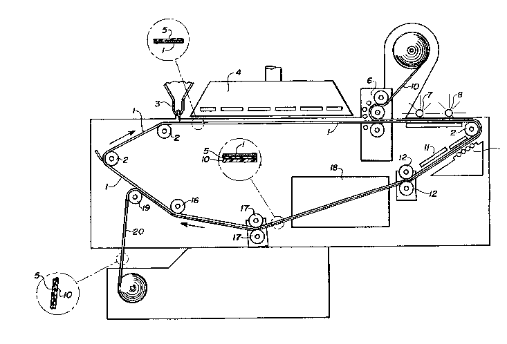
In figure 1 a printing system is shown having an
endless stainless steel or other conductive web or belt 1
which is driven by any suitable power means. This belt 1
is entrained about a series of primary rollers 2 and other
suitable supporting and guiding structureq. The belt 1 is
driven through a ~eries of electrographic stations which
are generally similar to those used in conventional
lS electrography or xerography, i.e. charge, develop and
fixing ~tations. However, in the present proceqs a
substantially thicker dielectric material is used and can
be coated on the belt 1 from solution, from a powder or
liquid formulation. While we will describe the dielectric
material as being coated from a solution, if suitable, the
dielectric may be added as a curable dielectric formulation
or as a dielectric as above defined. This coating iq
accomplished at deposition coating station 3. Station 3
can be any suitable dielectric dispensing means that can
provide any form of a dielectric suitable for the process
of this invention. After solution deposition at station 3,
the belt 1 with the liquid dielectric formulation thereon
-32-
2 ~ F3~ s~
i3 passed through an evaporation chamber 4 where the liquid
or qolvent of the dielectric formulation is removed,
leaving a white or colorlesq dielectric layer 5 on belt 1.
To ensure that layer 5 has a surface free of defects at
least one additional thin clear or white or other colored
dielectric film 10 may be provided at dielectric roll
station 6. It is intended that the dielectric 5 deposited
at ~tation 3 and the dielectric film 10 supplied at station
6 now provideq a final dielectric layer having a thickneYs
of up to about 10.0 mils. Present upon belt 1 now i~ a
two-layered dielectric material including dielectric layer
5 depo~ited at station 3 and dielectric film 10 deposited
at film ~tation 6. The ilm of dielectric 10 ~ay have a
built in adhesive material which can be activated by a
heater at film station 6. As will be described below in
figures 2 and 3, stations 3 and 6 may be used together or
separate from each other in the present system. Once
surface defect-free dielectric layers 5 and 10 are
deposited on belt 1, the combined dielectric layer is
surface discharged by corona discharge 7 to ensure an
electrically clean dielectric capable of accepting and
retaining the latent image charge. When the "dielectric
layer" is referred to in this figure 1 it is intended to
include layer~ 5 and 10. Once the dielectric layer has
been discharged by any suitable means, it is operatively
passed through image station 8 which comprises an apparatus
for generating charged particles in image configuration.
2~ ?~
These ions in imagewise configuration are extracted from
the print head at station 8 to form the latent
eLectrostatic image on the combined dielectric layers 5 and
10. The novel print head used in this invention is used
in a nitrogen or other inert atmosphere where exothermic
chemical reactions are prevented thereby substantially
reducing the operating temperature of the print head.
This increaqes the longevity of the print head and provides
improved performance. Also, an air knife is used with the
ion projection head which will prevent exposure of the ion
projection head to toner particles and/or solvents in
liquid toners by purging the space around the ion
projection head with solvent-free air or other gase~.
The dielectric layer containing the latent image is then
passed through a liquid toner at development station 9
where the latent image on it is made visible. It i9
preferred that the novel liquid toner used in the present
invention comprise~ a resin of the same family as the resin
uqed in dielectric layers 5 and lO. By using the same
family of resins in both the toner and the dielectric,
there i9 greater adhesion of the toner particle to the
dielectric layer. The toned image is then passed under a
heated platen 11 to evaporate the ISOPAR and/or other
solvent from the liquid toner. ISOPAR is a registered
trademark of EXXON. The dielectric layer may then be
pa~sed through heat or pressure fix nip rolls 12 where the
toned image is set or fixed to the dielectric. The
-34-
adhesive resin used in the toner in addition to the above
purpose, helps the toned particles adhere to each other and
t:o the dielectric layer 10. In a color system the above
process is repeated with sequential color stations until
the desired colored image is obtained and fixed. The
resulting dielectric layer may be used as a final product
or may be combined after separation station 19 with other
bases in post process steps. For example, a thicker bases
such as tile, wallpaper, fabric or the like may be adhered
to the under surface (non-imaged surface) of dielectric
layer. The resulting combined layer is passed through
temperature control chamber 18 which may be heated or
cooled or a combined heating-cooling chamber which with 11
evaporates the ISOPAR, fixes the toner and cools the
combined structure. The dielectric layer may then be
passed through pressure fix rolls 17 to further assist in
fixing the toner to the dielectric. At temperature
controlled separation roller 19 the final product is
separated from belt l. The final product 20, composed of
layers 5 and 10 is separated from belt 1 by cooling or any
other suitable means to separate it from belt l. This
generally occurs at 38 C or less when using the materials
of this invention. ~or those skilled in the art, other
formulations can be used which will affect the separation
characteristics from the belt wuch that release
temperatures will vary depending on the materials used.
Also, for those skilled in the art, it is obvious that for
~ g~ ~t~i
higher line speeds such as those greater than 30 ft/min.
ISOPAR evaporation can take place over a greater length of
t:ime. The cooling chamber 18 can be modified to be both a
heating and cooling chamber and in conjunction with heated
platen 11 all ISOPAR can be evaporated from the surface of
the dielectric substrate 10. For this case, pressure fix
nip rolls 12 can be opened and pressure fix nip rolls 17
can take their place. Also, partial fixing can take place
using both sets of pressure roller~ or any combination of
fixing steps involving 11, 12, 18 and 17. The final
product 20 is separated from belt 1 by a temperature
control means or any other suitable means to separate it
from belt 1. For materials which are formulated to be
subsequently heat reactivated types of adhesives as well as
dielectrics, separation from belt 1 can be enhanced through
the use of thin release coatings such as Teflon* FEP which
are a permanent part of the upper surface of the conductive
belt. It ic understood that Teflon is a registered
trademark of DuPont. These materials include non-porous
vinyl materials comprising polyvinylchloride, copolymers of
vinylchloride with minor portions of other materials such
as vinyl acetate, vinylidene chloride and other vinyl
esters such as vinylproprionate, vinylbutyrate, as well as
alkyl substituted vinyl ester~. Although the dielectrics
based on polyvinylchloride are preferred, the invention has
broad application to other polymeric materials consisting
of: polyethylenes, polyacrylate~ (e.g.
-36-
3 ~i
polyme~hylmethacrylate) copolymers of methylmethacrylate
such as methyl/n-butylmethacrylate, polybutylmethacrylate,
polybutylacrylate, polyurethane polyamides polyesters,
polystyrene and polycarbonates. Also, copolymers of any of
S the foregoing or mixtures of the foregoing may be used.
These materials can be used for the dielectric 5 or the
dielectric film 10 and they can be the same or different.
As earlier noted, the toned image can be fixed at station
12 by pressure, heat, spray, or other suitable fixing
methods. In any of these fixing methods, especially in a
multicolor system, the toner particle must be fixed without
substantially distorting the toner particle or the diameter
of the toner particle. Thi~ is important to maintain
optimum color quality and resolution of the final color
image.
The final product 20 removed at station 19 comprises
a dielectric layer 5, and a second dielectric layer 10.
The combined thickness of layers 5 and 10 is from 0.2 to
about 10.0 mils.
In figure 2 a dielectric solution or dielectric
liquid formulation is coated at station 29 upon an endless
conductive belt 1. The liquid formulation is controlled in
such a manner that upon evaporation of the solvent or
liquid therefrom a dielectric layer 23 having a final
thickness of from about 0.2 to about 10.0 mils remaining on
belt 1 and the surface of the dielectric layer is free of
defects. The solvent or liquid is removed by passing the
-37-
dielectric solution or formulation through an evaporation
chamber 21. Once the 0.2 to about 10.0 mil dielectric
coating is achieved, the surface i9 electrically discharged
by the use of a discharge corona 22 or other suitable
means. After being discharged the dielectric layer 23 is
charged in image configuration at ~tation 30 by the same
means as described in relation to figure 1. As the
dielectric layer 23 progresses forward bearing with it the
latent image, it passes through a developer station 24
where the latent image is toned and made visible. The
liquid from the toner is removed and the toned image may
be fixed by any appropriate means such as pressure, heat or
spray fixing at fixing means 25. Temperature control
chamber 26 which may be a combined heating-cooling chamber
can replace or assist the evaporation of the ISOPAR and
fixing of tne toner to the dielectric and assist or can
replace steps 24A and 25. After it is passed through the
chamber 26, the toned imaged dielectric 23 i9 pa99ed
through fixing rollers 34. The imaged fixed dieletric
layer is passed to cooling rolls 32 and 33 and
subsequently removed as the final imaged fixed product 28
at separation roll 33.
The endless belt 1 is then continuously moved to an
appropriate cleaning station 35 to remove any debris and i9
now ready to accept another layer of dielectric at coating
station 29.
-38-
.
2 ~ J '? ~
In figure 3 the same sequence of stepq as described
in figure 2 is followed except that rather than a
dielectric solution deposited at 29 in figure 2 upon the
endless belt 1 in figure 3, a spool 36 of a ilm dielectric
material supplies the dielectric layer 37 to the surface of
belt 1. ~his film 37 also can have a thickness of 0.2 to
10.0 mils and preferably is 0.2 to 1.5 mils. Film 37 i~
adhered to belt 1 by any appropriate means and the film
electrically discharged at station 38. Film 37 may have an
adhesive applied, if desirable. The dielectric film 37 is
then image charged at station 39 (by the same method as in
figures 1 and 2) toned or developed at developer qtation
40, toner may be fixed at fixing rollers or station 41.
The film is then advanced and pa~sed through stations 42,
43 and 47 in a similar manner as in figures 1 and 2. The
film is then advanced to cooling roller 48 and separation
roller 49 where the final product 50 is removed from belt
1. ~he endless belt 1 then may be cleaned by cleaning
blade or other mean~ 51 and is ready for accepting another
film coating of dielectric material and circulation through
another "imaging cycle", i.e. imaging, developing, fixing
and removal cycle.
In all of the described figures, means can be used
to recycle the dielectric layer to the same print head for
at least a second imaging at a point after the first image
fixing. This embodiment would be used in lieu of the
multistation system shown in figure 4. Therefore, each of
-39-
the system~ shown in figures 1, 2 and 3 can have any
conventional means to recycle the dielectric layer (after a
first image fixing) through the same stations, i.e. imaging
station or print head, developer station, developer or
toner liquid removal station and toner fixing station.
Figure 4 ~hows an imaging or printing system similar
to that described in figure 2 except in figure 4 a
plurality of imaging and toning or developing ~tations are
shown. In figure 4 a liquid dielectric is coated upon
endless belt 1 at coating station 52 and the liquid
evaporated off at drying chamber 53. A final dielectric
layer 54 up to about 10.0 mils now remains on belt 1. This
layer 54 is then surface discharged at discharge station 55
and image charged at print head 56. The latent image
formed at 56 is then passed to a first developer station 57
where a liquid toner of a first color i9 applied. The
liquid from this toner i9 removed at drying means 58 and
the resulting toned image fixed at fixing nips or roller3
59 or 66. Temperature control chamber 64 which may be a
combined heating-cooling chamber can replace or assist the
evaporatior. of the ISOPAR and fixing of the toner to the
dielectric 54 and assist or can replace steps 58 and 59.
The image may be fixed at fixing nip 59 or rollers 66. The
imaged dielectric layer 54 is then passed through discharge
stations 55 and print heads 71, 72 and 73 which create
latent images colorwise, and developer stations 60, 61 and
62 where different colored toners are applied and each
-40-
.:
-,
-- ,
,: :
~ `
fixed at fixing rollers 59. each toner at stations 57, 60,
61 and 62 will selectively respond to selective latent
image~ crea~ed by print heads 56, 71, 72 and 73 on
dielectric layer 54. A cooling roller 67 removes any heat
5from the resulting imaged layered structure and this
resulting structure passed to cool-separation rollers 68
where product 69 is removed from belt 1. Belt 1 is then
cleaned and prepared for another run or cycle.
For the sake of clarity, several components of the
10system are disproportionately illustrated in relation to
the entire system. Also, insignificant parts are not shown
in order that the main components can be clearly described.
In figure 5 an aluminum conductive substrate which
in this figure is a drum 74 is provided with any suitable
15means of power to rotate it upon demand. As indicated
throughout, conductive qubstrate 74 can be any convenient
substrate such as a conductive drum or an endless belt
moved around a drum, or a conductive substrate as earlier
defined, whichever i9 appropriate. A source of a
20dielectric film 75 is located in flow relationship to drum
74 and is fed thereupor. by a film dispensing mqans or any
suitable source 75. A dielectric film 76 having a
preferred thickness of about 0.5 to about 3.0 mils is fed
around film entrained roller 77 and over the surface of
25drum 74. The dielectric film used i8 a white dielectric
composed of poly(vinylchloride), however, any of the
above-noted dielectric materials may be used if suitable or
-41-
' ' ': ' ' ' : -
. .
2~g~
more appropriate. As the dielectric film 76 approaches
unit station A it is surface discharged by a discharge
means 78 to ensure an electrically clean dielectric layer
76 capable of accepting and retaining the latent
electrostatic charge. A discharge means 78, 83 88 and 93
may be used in the system before each station A-D if
de~ired. Once the dielectric layer 76 is discharged, it is
operatively advanced to station A where an ion print head
79 deposit~ a first charge thereon in image configuration.
While still at station A this latent image is contacted
with a black toner material from toner reservoir 80, said
toner deqignated BPA-06 manufactured by Research Labs of
Australia, Adelaide, Australia. After the black liquid
toner is attracted to the first latent image, a li~uid
removal or evaporation means 81 removes the liquid
component from the black liquid toner and the toner is
fixed upon the first latent image or first image at image
fixing means 82. Station A comprises components 78, 79,
80, 81 and 82. Conventional fixing methods such as
pressure fixing, spray fixing, heat fixing, combinations of
~hese or any other suitable fixing meanq may be u~ed at
fixing means 82. Once the first image has been fixed, the
dielectric film 76 is advanced to unit station B where a
second print head 84 deposits a second latent electrostatic
image upon dielectric layer 76. This second latent
electrostatic image on the dielectric layer 76 is then
advanced to a second toner reservoir 85 containing a cyan
-42-
2 ~
liquid toner. This second toner is made up of a toner
identified aq CPA-04 manufactured by Re~earch Labs of
Au~tralia, Adelaide, Auqtralia. After the cyan liquid
t:oner contacts the latent image and the toner particle~
therein are attracted to the qecond latent image, the
liquid component of the cyan liquid toner i~ removed at
liquid removal means 86 and the remaining toner fixed upon
the second latent (or now toner or developed) image by
fixing means 87. Station B comprises element~ or
components 83, 84, 85 and 86, 87 and all ~ubsequent
stations will be made up of similar components. At unit
3tation C the firqt and ~econd imaged dielectric layer 76
i~ image charged by a third ion projection head 89 to
p~ovide a third latent electrostatic image. This third
image is advanced to a third liquid developer or toner
reservoir 90 made up of a magenta color toner. Thiq toner
i~ designated MPA-02 manufactured by Research Labs of
AuYtralia, Adelaide, Australia. After the magenta toner is
attracted to the third latent image, the liquid portion of
the toner i3 removed at evaporation or liquid removal means
91 and the remaining magenta toner fixed in place at fixing
means 92. The imaged dielectric layer 76 i~ then advanced
to unit station D where a fourth latent electrostatic image
i9 deposited thereon by ion projection cartridge or head
94. Aq in previous stations, the imagewiqe information
is electrically communicated to each print head which then
respond~ with the corresponding image deposition of ions
-43-
2 ~
upon the dielectric layer 76. This fourth latent image is
moved to a fourth liquid toner reservoir 95 where a yellow
toner identified as YPA-03 manufactured by Re~earch Labs of
Australia, Adelaide, Australia is deposited in fourth
imagewise configuration upon the dielectric layer 76. The
liquid developer i9 then dried at liquid removal means 96
and the fourth image fixed at fixing means 97. The
resulting imaged film layers 76 may then be advanced as
product layer 105, dried at drying station 99 and removed
from the system at separation station 100.
Any number of unit station~ greater than one may be
used in the process and apparatus of this invention. An
important feature is to provide a system for color imaging
where the registration is simple and effective. This can
be done in the present sy tem with two or more images. An
additional step subsequent to air drying at drying station
99 may be used in the present system; that is, where a
thicker sub~trate is attached to the underside (non-imaged)
face of product layer 105. This substrate may be a base
layer used for example in tiles, wallpaper, ceiling
products or floor products and the like. This step is not
shown in the drawing since it and many other post-process
~teps may be used to combine product layer 105 with a
multitude of other materiais or objects. For ease of
handling, the dielectric film used in this invention is
preferably about 0.5 to about 3.0 mils thick, however, any
desirable or suitable thickness may be used. If desirable,
-44-
a poqt-~yRtem lamination step can be done if a laminated
product layer 105 is desired.
The preferred and optimumly preferred embodiments of
the present invention have been described herein and shown
in the accompanying drawing to illustrate the underlying
principles of the invention, but it i~ to be understood
that numerous modifications and ramification~ may be made
without departing from the spirit and scope of this
invention.
-45-
.
,