Note: Descriptions are shown in the official language in which they were submitted.
SELF~SYNCHRONIZING SERIAL TRANSMISSION
OE' SIGNALING BITS IN A DIGITAL SWITC~
ield of the Invention
The invention relates generally to the
transmission and reception of time division multiplexed
channelized data and more particularly to a method of
synchronizing to a serial data stream comprising coded
signaling data.
Background of the Invention
As is well known, digital telecommunication
systems in North America communicate with each other using a
standard basic format referred to as DSl (e.g. T1 carrier
system) or a multiple thereof wherein 24 voice channels are
multiplexed into a 125 microsecond time period called a
frame provlded by a basic 8 kHz sampling rate. Each frame
format provides for 24 channels each comprising one eight-
bit word along with one frame bit. In telecommunications,
signaling is a process of setting up a connection and
supervising its completion as well as monitoring the sanity
of the operating systems. In a DS1 data stream, signaling
information is imbedded in the digital stream of bits
representing the voice channels by using the least
significant bit from each channel (8-bit word) in every 6th
frame thus providing 24 bits every 6th frame which may be
used as a signaling channel. This encoding scheme results
in the use of only 7 bit words to encode the voice in those
channels; however, the overall distortion is not
significant. Signaling frames are provided for receiver
synchronization and to indicate even and odd 6th frames thus
providing a means for distinguishing between two types of
signaling bits, "Al' bits and "B" bits. A signaling frame in
the "AB" signaling scheme is comprised of 12 frames. Frame
6 corresponds to the "A" signaling channel and frame 12
corresponds to the "B" signaling channel. Instances occur
when more than two types of signaling bits are provided, as
3~
in the known extended "ABCD" signaling frame. In this
signaling scheme, the "ABCD" signaling frame is a superframe
comprised of 24 frames. Frames 6 and 12 correspond to the
"A" and "B" signaling channels and frames 18 and 24
correspond to "C" and "D" signaling channels respectively.
Generally the "A", "B", "C", and "D" signaling bits each
carry a different type of signaling information.
An alternative transmission scheme (PCM-30) uses a
32 channel format with channels 0 and 16 being used as
signaling channels. This transmission format uses a 16-
frame signaling frame with channel 16 of each frame being
partitioned in two parts each carrying one set of a, b, c, d
signaling bits, and channel 0 being used to transmit other
overhead information.
In contemporary telecommunication systems, it is
sometimes desirable to provide an interface circuit to the
carrier system for removing the signaling bits and
channelizing them into a serial bit stream for further
transmission along a single signal path.
As is generally known, there are numerous systems
for the redundant encoding of binary data; however, none of
them are suitable to provide self-synchronization to
serially transmitted "ABCD" signaling bits.
This invention is directed to a method and
apparatus for redundantly coding the channelized signaling
bits before their channelized transmission as well as a
method for decoding the received serial data stream in such
a way that the "ABCD" signaling bits are properly
regenerated and their association with the original
channelized data is maintained.
Accordingly, it is an object of the invention to
provide a system for the communication of channelized coded
data which exhibits robust self-synchronizing
characteristics.
It is a further object of the invention to provide
a system which will recover synchronization when incorrectly
coded data bits are transmitted.
r~
Summary of the Invention
In accordance with the invention, there is
provided a method of coding periodically occurring series of
signaling bits into a serial bit stream, comprising the
steps of a) replicating the first bit of each series a
predetermined number of times to yield a plurality of bits
each having the same value; b) concatenating to the right of
the plurality of bits a binary bit having the inverse value
to that of the first bit; c) concatenating to the left of
the plurality of hits a binary bit having a predetermined
value; and d) coding each of the remainder bits of each
series following the (a) and (b) steps above and replaclng
step (c) with the step of concatenating to the left of each
plurality of bits resulting from step (b) a binary bit
having a value inverse to said predetermined value.
Also in accordance with the invention, there is
provided a circuit for receiving and extracting signaling
bits from a data stream wherein the signaling bits are
encoded as described above, the circuit for receiving and
extracting signaling bits comprising a multiple level state
machine wherein each level corresponds to one signaling bit
to be extracted. Each level is responsive to the successful
extraction of a signaling bit at a previous level for
responding to the next available data from the data s~ream
for extracting therefrom the next signaliny bit. A
successful extraction of a signaling bit ~rom the last level
of the state machine indicates that the receiving circuit is
synchronized to the serial bit stream.
The invention permits the realization of a
transmission system for serial time division multiplexed
channelized data which exhibits self-synchronization between
the receiver and the transmitter. The invention also
permits the receiver to self-synchronize to the transmitter
even if occasional errors are transmitted assuming correctly
coded data is transmitted subsequent to the transmission of
error~.
2~3
:
Brief Description of the Drawings
An embodiment of the invention will now be
described in conjunction with the drawings in which:
Figure 1 is a block diagram of a transmission
system that includes a circuit for extracting and encoding
the signaling bits from a T1 signal lnto a coded serial
stream of bits and a circuit for decoding the coded signal
in accordance with the invention;
Figure 2 is a block diagram of the signaling data
encoder circuit shown in figure l;
Figure 3 is a logic block diagram of the decoding
circuit shown in figure 1; and
Figure 4 is a state diagram depicting the
operation of the decoding circuit of figure 3.
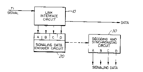
Figure 1 shows a link interface circuit lo
connected to receive a Tl signal. The circuit 10 includes a
signal decoder (not shown) adapted to extract the signaling
bits from the Tl data stream and provide a signaling encoder
circuit 20 with A,B,C, and D data streams. Of course, such
signal decoders are well known since they are employed in
conjunction with Tl data signals whenever the signaling data
embedded therein needs to be stripped off. The circuit 20
is responsive to the four data streams for providing a
serial coded signal for transmission to a decoding and
synchronizing circuit 30. The decoding circuit 30 provides
4 distinct ABCD signaling channels which may then be
deciphered as signaling data by a service controller and/or
reinserted in a Tl data stream. As described further below,
the signaling encoder circuit 20 performs data
transformation on the ABCD signaling bits prior to
transmission. Each of the signaling bits is encoded as six
bits in a T1 system and as four bits in a PC~-30
environment; the only difference being in the number of
replicated bits. These bits are used to ensure that the
number of coded signaling bits is compatible with the size
of the signaling channels of the two systems. In the
descri~ed embodiment, the A-bit is replicatsd to yield four
~ 2 ~ 6 ~ :~
bits each having the same valueO An inverse A-bit is then
concatenated to the right side of the four bits and a zero
bit is concatenated to the left side of the pair of A-bits.
A then becomes 0 A A A A (A-inverse). The B, C, and D-bits
are coded in the same manner as the A-bit except that, in
each case, a one bit is concatenated to the left side of the
four bits instead of a zero bit. Concatenating a bit to the
left side of the replicated bits which is of a different
binary state for the A-bit than for the B, C, and D bits
generates coded data which may be decoded with respect to
the coded bit to the left of the A-bit. The transmission of
a series of A, B, C, D signaling bits is thus as follows: o
A A A A (A-inverse) 1 B B B B (B-inverse) 1 c c C c (c-
inverse) 1 D D D D (D-inverse). It therefore requires 24
bits to transmit 4 signaling bits serially in a time
division channel. It should be realized that exchanging the
one bits and the zero bits in each series of signaling data
yields a data stream that is also recoverable by the
receiving circuitry. Of course, the encoder circuit also
includes circuitry to serialize and transmit the coded
signaling data.
Figure 2 illustrates a portion of the signaling
encoder circuit 20 adapted to perform the encoding of an A
signaling bit. A replicating circuit 22 receives the A bit
from the decoder circuit lo and provides a right
concatenating circuit 23 with four identical A-bits. The
latter provides a left concatenating circuit 24 with five
bits, the right most bit being the inverse of the replicated
bits, and the circuit 24 concatenates thereto a bit having a
predetermined binary value. Of course, the encoder circuit
20 also includes circuitry identical to circUits 22, 23 and
24 for the coding of B, C, and D bits.
The output signals of the left concatenating
circuits 24 are connected to a parallel-to-serial converter
25 for conversion of the coded data into serial coded data.
Thus, the coded data corresponding to four signaling bits
may be transmitted in a serial data stream corresponding to
.. .. . .
7 :~
one Tl channel. It will of course be realized that circuits
22-25 may be implemented using very few logic gates; in
fact, circuits 22 and 24 may consist of logic connections
only whereas circuit 23 requires a single inverter gate for
its implementation. The circuit 25 on the other hand may be
a commercially available parallel/serial converter circuit.
It will also be realized that the sequence of coding any one
bit is not important. The same coded data may be achieved
by changing the order of the coding steps illustrated in
10 f igure 2 .
:::
`~;` Figure 3 is a logic diagram of the circuit 30
adapted to perform the decoding of the encoded signaling bit
stream generated by the encoder circuit 20. A flip-flop 31
receives and temporarily stores each of the coded signaling
bits as it is received at a receiving terminal. A logic
circuit comprising a ROM 33 and a 4-bit state register 34 is
responsive to each stored signaling bit and the previous
content of ~he register for providing the state register 34
with a 4-bit signal corresponding to a next execution state.
A selection circuit for selecting the signali~g bits from
` the coded data stream comprises a binary decoder 35 and 4
one-bit latches 36, 37, 38, and 3~. The binary decoder 35
is responsive to the two most significant bi~s of the 4-bit
signal of the state register 34 and to a clock signal CK
derived from the output of an AND gate 41 having as its
input signals the two least significant bits of the 4-bit
signal and an external clock signal to provide latches 36,
37, 38 and 39 with 4 distinct latch enable signals. The
clock signal also serves to clock the state register 3~.
The latches 36, 37, 38 and 39 are also connected to the
output of the flip-flop 31 through an inverter gate 32.
In operation, the flip flop 31 receives and stores
each bit of the coded data and each signaling bit is used
for selecting one of two memory banks (not shown) within the
ROM 33. Read-only data coded within the ROM 33 forms a
table to point to subsequent states in dependence upon the
state of the input signals comprising ~he 4-bit signal and
2 ~ 4 ~
the stored value within the flip-flop 31. The state
register 34 latches the value of the next execution state
pointed to by the ROM 33. The output signals of the state
register are used to address memory locations within the ROM
33 and a feedback path is formed between the ROM 33 and the
state register 34. The two most significant bits of the
output signals from register 34 are decoded by the binary
decoder 35 to provide latch enable signals for the latches
36, 37, 38 and 39. upon the assertion of one of the latch
~nable signals one of the latches stores the inverted
current bit stored within the flip-flop 31. The bits stored
in the latches 36, 37, 38 and 39 are available for use by
service circuits or the like and/or may be inserted in a T1
data stream.
Figure 4 is a state machine diagram illustrating
the operation of the circuit shown in figure 3. Sixteen
execution states are shown; states 0 through 14 each provide
a pointer to a subsequent state and states 1, 2, 5, 6, 9,
10, 13 and 14 e~ch provide an additional pointer to
themselves when the value of the received bit in one of
those states remains unchanged from the value upon entering
that state. States 3, 7, and 11 each provide a pointer to
subsequent states and also provide a pointer to state 0.
The pointer to state 0 is the selected execution path when
synchronization has not yet been achieved. State 15
provides a pointer to state 0. The system has synchronized
when the value of the received bit in state 15 is a 1.
Determining the binary value of the coded bit in state 15
allows one to know that the system is synchronized. Once
the system has synchronized, the A, B, C, and D bits are
latched in states 0, 4, 8, and 12 respectively. A 4-state
logic state machine 60 is shown having a feedback ~xecution
path and, a feed-through execution path to a subsequent 4-
state logic state machine 61. Of course, it should be
realized that, in an "AB" signaling bit arrangement, eight
execution states are required with state 7 providing a
pointer to state 0. In such a system synchronization occurs
7~
~: 8
when the value in state 7 is a 1.
. TAE3LE 1
STATE REG STATE REG
5 1 l
V V
., REC'D REC'D
ADDR sIT cURRENT NEXT ADDR BIT CURRENT NEXT
`~ 10
o 0 0 1 16 1 0 2
1 0 1 1 17 1 1 3
A 2 0 2 3 A 18 1 2 2
3 o 3 0 19 1 3 4
. .~
4 0 4 5 20 1 4 6
0 5 5 21 1 5 7
B 6 0 6 7 B 22 1 6 6
7 0 7 0 23 1 7 8
a 0 8 9 2~ 1 8 10
9 0 9 9 25 1 9 11
25 C 10 0 10 11 C 26 1 10 10
11 0 11 0 27 1 11 12
12 0 12 13 28 1 12 14
13 0 13 13 29 1 13 15
D 14 0 14 15 D 30 1 14 14
15 0 15 0 31 1 15 0
. .
Table 1 is a representation of programmed data
within the ROM 33. The address column shows 32 memory
locations each one being addressable by 5 address bits.
Functionally, the 32 memory locations are divided into two
banks of 16 memory locations; each bank being selected in
dependence upon the state of the output signal of the flip-
flop 31 which is connected to the most significant address
bit of the ROM 33. The output signals from the state
register 34 address the 4 least significant address bits of
the ROM 33 thereby providing an addressable range of 16
addresses in each bank of the ROM.
It is also possible to encode and decode the data
using a commercially available microprocessor; however,
7 ~
encoding and decoding at the required speed may not be
practi.cable. Numerous other modifications, variations and
adaptations in particular, time multiplexing of the circuit
. to encode/decode signaling bits for all channels of one or
several Tl signals may be made to the particular embodiment
of the invention described above without departing from the
scope of the claims.