Note: Descriptions are shown in the official language in which they were submitted.
2041 706
MONOLITHIC INTEGRATED
OPTICAL AMPLIFIER AND PHOTODETECTOR
Technical Field
The present invention relates to semiconductor optical amplifiers and, in
5 particular, to an optical amplifier integrated on a substrate together with a monitoring
photodetector.
Ba-~k~round of the Invention
Conventional long haul communication systems comprise both optical
and electronic components. For example, repeaters detect light photoelectrically,
10 amplify the resulting current electronically and then use the amplified current to
drive a semiconductor laser that reconverts the electrical signal back into an optical
signal. The optical signal is then injected into an optical fiber to the next repeater in
the system where the conversion from optical to electrical and back again to optical
is repeated again.
In an all-optical tr~n.cmi~ion system, light once generated will be
transmitted optically, received by optical detection and, more importantly, amplified
optically such that there is no intermediate conversion from optical to electrical and
then back to an optical form. Optical amplifiers afford direct optical amplification
of an optical signal, which results in the elimin~tion of the electronic processing.
20 Accordingly, optical amplifiers will enable optical communication systems to have
repeaters which have higher bandwidths, are physically smaller, simpler in design,
more efficient to operate and more economically to produce.
Furthermore, with the performance of optical amplifiers relatively
unaffected by changes in data bit rate or by the presence of additional channels at
25 separate wavelengths, optical amplifiers will become key components in lightwave
tr~n~mi.~.~ion and switching systems. Unfortunately, although optical amplifiers are
integrable with other opto-electronic devices in photonic integrated circuits (PICs), it
has been problematic to control the output power because the gain of an optical
2041 706
- 2 -
amplifier can be affected by both environmental effects, such as changes in source
wavelength and polarization, as well as temperature variations and amplifier
degradation. Accordingly, integrating a monitoring detector with the optical
amplifier to monitor the output power thele~ol" seems to be a reasonable solution,
5 other than 1~tili7.ing bulk detectors and couplers, which are prohibitively lossy and
expensive.
Unlike a semiconductor laser wherein a detector may be positioned on
the back facet, no facet of the optical amplifier is available because both front and
back facets are employed for ingressing and egressing optical radiation. As such, the
10 only viable alternative is to employ an integrated branching waveguide, such as a
Yjunction waveguide, to tap a fraction of the output power to monitor the amplifier.
Because the injected optical radiation into the optical amplifier can be afl~ ily
polarized, the power splitting ratio of the branching waveguide should be
polarization invariant in order for the photogenerated current of the integratedlS detector to be used in a feedback configuration. Disadvantageously, optical
amplifiers require more than 40 dB of optical isolation in order to suppress ripples in
the gain spectrum resulting from residual Fabry-Perot resonances. Alternatively
stated, the back-reflectivity of the Yjunction waveguide should be substantiallysmaller than the residual reflectivities of the anti-reflective coatings on the end facets
20 of the optical amplifier.
Due to fabrication limitations, practical Y-Junction waveguides have
truncated wedge tips. See, for example, Sasaki et al., Electronics Letters, Vol. 17,
No. 3, pp. 136-8 (1989). That is, a blunted Yjunction tip, which results in a
substantial amount of optical back-reflection to the optical amplifier which has,
25 because of deleterious effects to the amplifier, prohibited the monolithic integration
of a coupled optical amplifier and monitoring photodetector via an optical branching
wavegulde.
Summary of the Invention
In accordance with one aspect of the invention there is provided a device
30 comprising a photodetector, first and second interconnecting waveguides, and an
optical amplifier coupled via at least one of said waveguides to said photodetector,
204 1 706
- 2a -
each integrated on a common semiconductor substrate, said second waveguide
intersecting and coupled optically to said first waveguide to form a Yjunction
having a truncated wedge tip, said Yjunction having a junction region located
between said first and second waveguides, and a gradient in the effective refractive
5 index coupled to said junction region along the axis of optical propagation of said
first waveguide so as to reduce the difference between the effective refractive indices
at the optical int~ ce of said truncated wedge tip for reducing back reflection of
optical radiation from said optical amplifier incident on said truncated wedge tip.
In accordance with another aspect of the invention there is provided a
10 device comprising a photodetector, first and second interconnecting waveguides, on a
laser coupled via at least one of said waveguides to said photodetector, each
integrated on a common semiconductor substrate, said second waveguide intersecting
and coupled optically to said first waveguide to form a Yjunction having a truncated
wedge tip, said Yjunction having a truncated wedge tip, said Yjunction having a
15 junction region located between said first and second waveguides, a gradient in the
effective refractive index coupled to said junction region along the axis of optical
propagation of said first waveguide so as to reduce the difference between the
effective refractive indices at the optical interface of said truncated wedge tip for
reducing the back reflection of optical radiation from said laser incident on said
20 trllnc~tecl wedge tip, and feedback means jointly coupled to said photodetector and
said laser to control the optical output power of said laser.
More specifically in this invention, an optical amplifier and a
photodetector are integrated on the same semiconductor substrate, the
photodetector being optically coupled to the optical amplifier via a branching
25 waveguide having low radiative loss and low back-reflectivity. Importantly, due to
the low back-reflectivity, the branching waveguide is able to redirect a small portion
of optical radiation from the optical amplifier to the photodetector without
deleteriously affecting the performance of the optical amplifier. In particular,the branching waveguide is realized by employing between the branches of the
30 waveguides, a junction region having a gradual decrease
~;
2041706
in effective refractive index such as to dcclease the di~çence bet~n the crrecli~e
lc~iac~ e indices at the optical interface of the tmnc~t~ wedge tip as seen by optical
r~ tion inri-l~nt thereto from the optical amplifier.
Advantageously, the ability to monolithir~lly integrate a photodetector
S and an optical amplifier affords an in-situ means to monitor the thic~kn~ss of thin-film
co~ting~ deposited on the end facets of the ~mplifi~r. That is, the coating thir~n~ss
may be optimized by m~ximi7ing the current from the photodet~tor.
With the gain of the optical amplifier dependent on the polarization of
ingressing optical radiation, the device may further be used to measure the state of
10 polarization of ingressing optical radiation incident on the optical amplifier.
Brief Description of the Drawin~
A more complete understanding of the invention may be obtained by
reading the following descliplion in colljunclion with the appended drawing in
which:
FIG.l shows a pel~ecli~e view of an integrated optical amplifier, Y-
junction waveguide and photodetector in accordance with the present invention;
FIG.2 shows a longit-~-lin~l cross section of the optical amplifier, the
photodetector and the Yjunction waveguide illustrated in FIG.l;
FIG. 3 shows a top plan view of the Yjunction waveguide illustrated in
FIG.l.
FIGs.4,5, 6, 7, and 8 show the effective refractive index profiles (X-
axis) of the Yjunction waveguide of FIG. 3 for various planes along the Z-axis;
FIG.9 shows a sche,llalic diagram of the integrated structure of FIG.l
in an fee~b~c~ configuration with an external feedb~c~ loop for controlling the
optical power output of the optical amplifier;
FIG.10 shows the stabili~d output power versus time profile for the
fee~3b~c~ configuration illustrated in FIG. 9;
FIG.ll shows the light versus current profiles for the integrated
structure of FIG.l before and after anti-reflective coating an end facet; and
FIG. 12 shows the output power versus input polarization profile for the
integrated structure of FIG.l.
20~Q6
Detailed Description
Optical arnplifiers may be used in long-haul optical fiber co.. ~ ir~ti--n
s~s~.lls where the info....~ion being tr~ncmitte~1 is ,~p~sented by encoded optical
r~diation which propagates through optical fibers. For error-free tr~ncmicsion, the
S intensil~ of the optical radiadon should be m~int~ined within a predele.milled range,
which is normally ~co..~plished by diverting some of the optical r~ tion from the
optical amplifier to a ~..onilo.;ng photodetPctor. In the prior art, the optical amplifier
and photodet~-lol are sep~l~ and distinct from each other, coupled externally by a
bulk lossy fiber coupler. The monilo,ing photodetector measures the average power
10 output from the optical amplifier, with a signal generated thereby to control a
feedb~r~ circuit in order to adjust the optical output power within a desired
predetermined range. Importantly, the control of the optical output power of theoptical amplifier is necessary to compe~C~te for en~ilo.. ellt~l variations, such as
changes in source wavelength and polarization, ~m~l~tu~ variations and amplifier15 degr~l~tion~ Although a separate monilo.ing photodetector is adequate for most
application, it is highly desirable to have a photodetector integrated with the optical
amplifier on the same semiconductor chip.
In this invention, an optical amplifier and moni~o,illg photodetector are
monolithir~lly integrated, with the photodetector being optically coupled to the~0 optical amplifier via a branching waveguide having negligible back-reflectivity.
tly, the br~nching waveguide, which exhibits low radiative loss as well as
low back-reflectivity, is realized by employing b.,l~,.~n the branches of the
waveguide a junction region having a gradual decrease in the effective refractive
index along the direction of optical prop~gation In particular, this approach
25 .~ini~ es the effect of wedge tip tnlnr~tion seen for incident optical radiation from
the optical amplifier by reducing the dirÇ~lence in the refractive indices at the optical
in~.r~ce of a trunrat~l wedge tip. It should be noted that the effective refractive
index in the junction region between the branches specifically varies from the core
index to the nominal cladding index of the branching waveguide. Advantageously,
30 the low-reflectivity from the trunrated wedge tip allows the optical amplifier to be
monolithir~lly integrated with and coupled to a mo~ o. ing photodetector because of
the high optical icol~tion arrol~led by the branching waveguide's low back-
reflectivity.
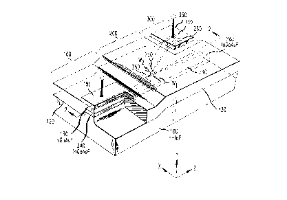
Turning to FIG. 1, there is shown a pcl~i./e view of an integrated
35 optical amplifier 100 and ll-onilolil-g photodetector 300 in accordance with the
principles of the invention. A low loss, low reflection asymmetric Yjunction
2Q417D~
waveguide 200 optically coupled to amplifier 100 redirects a portion of the optical
radiation from optical amplifier 100 to ll~onitoling photodetector 300 with negligible
back-reflection. The integration of optical amplifier 100 and photot1~tector 300 is
pre~1ir~te~1 on the ability of Yjunction waveguide 200 to divert a portion of light
5 from optical amplifier 100 to photodetector 300 without subst~nti~lly reflecting any
optical r~ tiQn from the tr~nc~tçcl wedge tip back to optical amplifier 100. Typical
lengths for ~mplifier 100, Yjunction waveguide 200 and photodetector 300 are 850~m, 1640 ~lm and 170 ~m, respectively.
Optical amplifier 100, photo~etector 300, and Yjunction waveguide 200
10 are fabricated on n-type, InP substrate 160. In general, in order to fabricate Y-
junction waveguide 200, it is generally ne~ess~ry for the effective refractive index of
the material surrounding the waveguiding regions (the cladding) to be less than the
effective refractive index of waveguiding regions (the core) such that the structure
can guide optical radiation of the applupliate wavelength from optical amplifier 100
15 by means of total intern~l reflection to photodetector 300. Yjunction
waveguide 200 com~lises straight output branch 240 and side branch 260 having a
3.5 ~ bend thereto.
Integrated optical amplifier 100, photo~etecLor 300 and Yjunction
waveguide 200 are fabricated from III-V semiçoll~uçtor materials. Other
20 semiconductor materials, however, may be utilized which have applupliate refractive
in~ices Standard fabrication techniques such as melta-organic chemical vapor
deposition (MOCVD) and regrowth, wet chemical etching, and photolithography are
employed to fabricate the structure. These fabrication techniques are well-known to
those persons of ordinary skill in the art and, thus, not ~ cu~se~l in~detail here.
In the ill~ ali~.e embo liment shown in FIG. 1, optical amplifier 100 is
optical coupled to p-i-n photodetector 300 via Yjunction waveguide 200. Optical
r~ tion which impinges on the front facet of optical amplifier 100 is amplified by
active InGaAsP layer 130 (1.3 ~m bandgap layer). Moreover, the confined optical
rarli~tion is then coupled to ~(ljaçent InGaAsP passive straight branch waveguide 240
30 (l.lllm b~ndg~p layer), extending from and underlying active InGaAsP layer 130, as
shown in FIG. 2 illustrating the cross sectional thereof. It should be noted that active
InGaAsP layer 130 is removed from passive waveguide areas. Straight branch
waveguide 240 is used as an output port while side branch waveguide 260 extends to
and underlies active InGaAsP layer 330 (1.3 ~m b~n~g~p energy layer), optically
35 coupling about 10 % of the incident optical r~di~tion to p-i-n detector 300. Similar
to a portion of straight branch waveguide 240 in the active amplifier section, side
2041~Qfi
- 6-
branch waveguide 260 in a portion of the photodetector section is ~ cent to active
InGaAsP layer 330 for coupling optical radiation to photo~Pt~ctor 300. It should be
noted that the location of buried Yjunction waveguide 200, that is straight and side
branch waveguides 260 and 240, are shown projected on the top surface by dotted
5 lines.
Both side and straight branch waveguide 260 and 240, respectively, are
passive InGaAsP (1.1 ~m bandgap) waveguide mesas buried by a semi-insulating
InP region 120. Angles other than 3.5 ~ between the branches may be used for
dirr~,r~. t desired power splitting ratio. Generally, the power splitting ratio is
10 controlled by the widths Wl and W2 of straight branch waveguide 240 and side
branch waveguide 260, respec~ively, and the angle ~ between the branches. For
higher optical power propag~ting to straight branch waveguide 240 than side branch
waveguide 260, the width W2 should be narrower than the width Wl. Furthermore,
the angle may be chosen in accordance with the desired power division and is,
15 generally, limited to a few degrees because of fabrication limit~tions and bending
loss considerations.
Impol~ntly, a gradual change in the effective refractive index along the
Z-axis in junction region 280 between side branch 260 and straight branch 240 isemployed to reduce the effect of the wedge truncation seen by optical radiation
20 egressing from optical amplifier 100. Typically, the lef~d~;live effective index of
junction region 280 has a linear gradient index profile along the Zaxis, varying from
the core index to the cladding index of straight and side branch waveguides 240 and
260, ~ ively. Other profiles may, however, be employed such as a parabolic,
e~ponential or step function profile. It is contemplated that in the~ fell~,d
25 elnbo~ , both side and straight branch waveguides are single mode waveguides.A semi-ins~ ting blocked planar buried h~,t~,ro~ cture (SIPBH)
waveguide with an active InGaAsP layer (1.3 ~m b~ndg~p energy) structure is
employed for both optical amplifier 100 and p-i-n photodetector 300. A Fe doped
semi-in~ ting InP region 120 is used for both current blocking and transverse
30 optical confinement in optical amplifier 100 and photodetector 300. Note that the
- active layer is l.,~ ,d for passive Yjunction waveguide 200 and, thus, optical
amplifier 100 and photodetect-)r 300 are similar to Yjuncdon waveguide 200 except
for acdve InGaAsP layers 130, 330 and p conducdvity type layers 150, 350, which
facilitate electrical contact to the resl)e~ive acdve InGaAsP layers.
7 20~17~6
Ll.pol~1tly, juncdon region 280 hetween the branches of the Yjuncdon
has a gradual change in the effecdve l~ir ~;l~e index along the Zaxis, as discussed
aho~ehe.~ , to reduce the effect of the wedge dp trunr~hon seen by an opdcal mode
prc~p~g~ting therein from opdcal amplifier 100. This may be accomplished, as is the
5 case here, by a gradual decrease along the Z-axis in thicknes~ of an InGaAsP region
in Yjuncdon region 280 underlying InP region 120. Semi-insuladng InP region 120
is also used for a top passive cladding waveguide region because it has a smaller
absorption loss coefficient than p conducdvity type layers 150, 350. As an example,
passive InGaAsP straight and side waveguides 240 and 260, respecdvely, and active
10 InGaAsP layers 130, 330 have respective thickness of 0.35 ~m and 0.9 ~um.
Moreover, the widths of both the acdve and passive waveguides outside Yjuncdon
area 290 are 2.5 ~lm.
In FIGs. 3, a top plan view of Yjuncdon waveguide 200 is illustrated.
For convenience of description, the direcdon from straight waveguide 240 toward
15 side waveguide 260 is taken as the Z-axis and the direcdon perpendicular to the
plane of the drawing is taken as the Y-axis in order to define a X-Y-Z coordinate
system, as shown in FIG. 3. The 2.5 ~lm width W of the straight branch
waveguide 240 is tapered by a 80 ~lm t~pering length for ~ b~hc mode propagationinto Yjuncdon area 290. Power division occurs by mode conversion at the Y-
20 juncdon, with the modal behavior domin~te~ by the abrupt transidon at the truncatedwedge dp 210. The widths of the waveguides at junction dp 210 are 2.2 llm and 3.3
~m for side branch waveguide 260 and straight branch waveguide 240, respectively.
Further, the width of trllnr~tefl wedge tip 210 is 0.8 ~lm. In this exemplary structure,
the widths of both waveguides are tapered back to a width W of 2,5 llm at about 100
25 ~lm outside of the Yjuncdon tip, as shown in FIG. 3.
The integrated structure of optical amplifier 100, p-i-n
pholod~ teclor 300 and Yjuncdon waveguide 200 is reali~d by three epitaxial
growth steps and by convendonal photolithography and wet chemir~l etching. That
is, a planar metal-organic chemical vapor depo~ition (MOCVD) growth for InGaAsP
30 active layers 130, 330 and InGaAsP passive waveguide layers 240, 260 followed by
two MOCVD regrowths for blocking layers 120 and cap layers 150, 350. After
acdve layers 130, 330 and passive waveguide layer 240, 260 are grown on n-type
InP substrate 160, 2-3 llm wide mesas are etched using a SiO2 mask in order to form
active regions 130 and 330, and straight branch region 240 and side branch
35 waveguide 260. In particular, Yjunction waveguide mesas and the active
waveguide mesas are etched using a SiO2 mask with the straight sections parallel to
20~17Q6
- 8 -
the [011] orient~ion It should be noted that passive Yjunction waveguide 200 will
be similar to the active section, that is optical amplifier 100 and phot detector 300,
except for active layer 130, 330 and cap layers 150, 350. Typically, the total height
of the active waveguide mesas are 1.5 -2 ~m, and the height of the Yjunction mesa
5 is less than 1 ~lm. Next, a MOCVD l~lUWlll iS pe.rwll,ed for forming semi-
inslll~ting block InP region 120. The active waveguide is completely planarized
with semi-insul~ting ~P region 120, while the passive Y-branch is covered thereby.
The SiO2 mask is removed and cap layers 150, 350 grown by MOCVD over active
regions 130 and 330 of optical amplifier 100 and photodetector 300, respectively.
10 Cap layers 150, 350 consist of a 1.5 llm p-InP layer followed by a 0.5 ~m p+ InGaAs
layer.
In order to obtain the effective refractive index profile along various
points of the Yjunction waveguide as shown in FIGs. 4 through 8, the processing
steps are dirr~,lel-t than conventional photolithographic steps. The passive InGaAsP
15 between side branch waveguide 260 and straight branch waveguide 240 is only
partially removed by a shallow etch when defining waveguide mesas 240 and 260, as
discussed above. With the side and straight branch waveguides defined by silicondioxide mask and the shallow etched Yjunction area covered by photoresist, a
second deep etch produces the passive InGaAsP waveguide mesas. The thicknecs of
20 the shallow etched InGaAsP layer which remains belw~en the two branches is 0.211m
and tapers to ~ro over a length of 100 ~lm from Yjunction tip 210. The regrowth of
semi-inc~ ting InP region 120 over the InGaAsP layer buries the passive
waveguides, giving the effective refractive index shown in FIGs. 4 through 8.
Active layers 130, 330, however, are subsequently covered by a third MOCVD
25 growth of the p-InP and p InGaAs contact layers as rliccucse~l above. These layers in
the passive waveguide and Yjunction areas are subsequently removed by chemical
etching All the etching steps above are done using standard selective etchants, such
as a 2:1 Il~ib~lult of HCl:H3PO4 for InP and a 3:1:1 mi~ of H2SO4 H202:H20 for
InGaAsP and InGaAs.
Those persons skilled in the art will readily note that optical
amplifier 100 is formed by depositing antireflective coatings on the end facets.However, it is further conte ~Iplated that optical amplifier 100 may be made into a
laser either by integrating a grating in order to provide distributed feedb~rl~ or by
utilizing the Fabry-Perot l~son~nces from the end facets, if made to have a
35 sufficiently high l~ne~ ity. See, for exarnple, K.Y Liou et al., Appl. Phys. Lett.
Vol. 54 No. 2 pp. 114-6 (1989).
9 201170fi
In operation, the current of photodetector 300 tracks the optical
Arl~rlifier output power. FIG. 9 illustrates a sche .-~tir of an external fee~bac~ circuit
that was added to integrated structure 10 to permit the output power to be
A~ltom~tir~lly ~ inlAin~l con~t~nt over a specifierl range of input power levels and
S pol~ri7~tion Feedbac~ circuit 500 co~ al~,s the current from photodetector 300with a reference value at dirre,cnlial ~mrlifiçr 510 that adjusts the bias current to
optical AmplifiPr 100. Shown in FIG. 10 is the recorded trace of the amplifier output
power as stabli_ed by fee~b~ circuit 500. It should be noted that a con~tAnt output
power of 3.5 mW is ~lemon~trated with the input power (> 30 ~W) allowed to vary
10 and the input polarization allowed to rotate about +/- 25 ~. Alternatively, since
integrated Yjunction waveguide 200 is pol~ri7~tion independent, while optical
amplifier 100 is polarization depen-lent, a fiber polarization controller 520 may be
utilized to optimize the optical gain by maximizing current from photodetector 300.
That is, polarization controller 520 may be o~l~lcd electrically via feedb~clf
15 circuit 500 such that the peak phol~-ull~nt can be used to aulolll~l;r~lly m~int~in
m~illlUIII amplifier gain.
Before anti-reflective coating the end facets of the structure of FIG. 1,
optical amplifier 100 operates as composite-cavity laser, having ap~lo~dmately athreshold current of 80 mA at 22 ~ C. FIG. 11 illustrates the typical photocurrent
20 generated by unbiased photodetector 300 as a function of the amplifier bias current
Ib before and after anti-reflective coating an output facet of integrated structure 10.
By coating both facets, a traveling wave amplifiçr is formed. With an injected
current of 130 mA into optical amplifier 100, the spontaneous emission spectrum
exhibits ripples of - 0.4 dB due to residual Fabry-Perot reson~nces, with mode
25 s~al~lion of 0.9 A. This clearly in~icates only residual reflections from the two
facets occurs and, more im~l lantly, that negligible reflection occurs at the Y-juncdon tip. Injecting optical r~di~tion (1.311m wavelength) into active InGaAsPlayer 130, the optical signal gain versus injection current was Ille~wcd for both the
TE and TM cases. These measule.llel.ls in-lic~tç applo~-imately a 20 dB gain for TE
30 pol~ri7~tit~n~ with the signal gain a few db less for TM pol~ri7~tion.
It is to be understood that the above described invention is not limited to
an optical amplifier, but can be also be used with other devices. Regardless of the
specific device use, it is illl~Ol lant to be able to monitor and control the output power
of the device. Clearly, device structures that incorporate a detector on the same chip
35 as an optical amplifier or the like are illlpul ~1t beccause such integrated devices can
provide the full benefits which result from integration, such as c~ mp~tnçss,
-
20~17Q6
- 10-
reliahility, low cost, and high pe.ro....Ance
It is important to realize that for the structure to be made into an optical
amplifier, the end facts of the device must be anti-reflective coated. Otherwise, if the
facets of the structure are partially reflective, sl,ol-lAnf,ou~ emission that results from
S current injection will resonate back and forth with each pass to produce lasing. As
such, optical amplifiers are critically dependent on the residual reflectivity because
any residual reflection causes ripples in the gain spectrum as a result of Fabry-Perot
csonAnces. Currently, the end facets of prior art optical amplifiers are anti-reflective
coated by thin film deposition. A primary disadvantage of this methods is that the
10 thickness of coating for opLilllulll p~lrollllance cannot be accurately monitored in-
situ by an external photodetector.
The ability to monolithirally integrate a photodetector with an optical
amplifier affords an in-situ anti-reflection coating technique. The coating mAteriAl
may be applied to an exposed facet while the amplifier is biased. In operation, the
15 oplilllulll anti-reflective coating thickness is dete.lllined when the photo gellel~ted
current from monitoring detector 300 reaches a .. .i~ "~, for a specific bias current,
according to the graph shown in FIG. 11. Note that if a high reflective coating is
desired, such as for lasing, the coating thir~nçss may be optimi~d by maximizingthe pholocullcnt from photodetector 300.
Illustrated in Fig. 12 is the variation of the amplified output power with
rotation of the input polarization. Electrically controlling the polari~r in a feedback
configuration by the photocurrent reali~s a polari_ation feedbac~ loop which
ope,~tes automAtirAlly to mAintAin a m~illlulll amplifier gain if the photocurrent is
ma~cimi7~d Additionally, as illustrated by FIG. 12, the photocurrnt generated is25 highly dependent on the polarization of the ingressing optical radiation. Thus, it is
possible to measure the degree of polarization by correlating the photocurrent to the
state of polari_ation vis-a-vis FIG. 12. That is, a polarization detector can berealized by lltili7ing the device of FIG. 1 and measuring the generated photocurrent.
Of course, this A~sumes that the measured photocullcnls are normAli7~