Note: Descriptions are shown in the official language in which they were submitted.
~- 20~1753
The present invention relates to a procedure for
regulating the d.c. voltage of a pulse-width modulated
rectifier bridge controlled by self-commutated
semiconductor components.
Pulse-width modulated mains rectifier bridges are
used to feed a constant-voltage load, which is connected to
the d.c. terminals of the rectifier. Such a load may be
e.g. an inverter provided with a constant-voltage
intermediate circuit, used to feed an elevator motor. The
characteristic features of such rectifiers include two-way
power flow and, due to pulse-width modulation (PWM), low
distortion levels for the currents in the supplying
network.
Previously known procedures are based on the use
of phase voltages measured via transformer circuits to
produce either the current references for a rectifier
working on the principle of two-position control, or the
voltage references for a PWM rectifier. In both cases, the
disturbances materialized in the phase voltages are
directly transmitted to the modulation references and
therefore to the currents taken from the network. This
involves a deterioration of the characteristics of the
rectifiers, especially in industrial networks where as it
is well known, the voltages are distorted. Moreover, when
a two-position control is used the rectifier voltages and
currents contain harmonics which extend over a large
frequency range and are therefore difficult to filter. In
addition, for both methods, each phase voltage requires its
own regulation circuits, thus increasing the complexity of
the systems.
In the method of the invention, the modulation
references are produced using pure sine and cosine curves
synchronized with the mains voltages, spatial vectors
formed from them or with components of such vectors by
means of a phase-locked loop. This ensures that mains
voltage distortions will have no effect, via the modulation
'~C
2041753
references, on the mains currents. On the other hand, the
regulation is effected in a coordinate system tied to the
spatial vector of the mains voltages, allowing regulation
of the d.c. components. Thus, it is not necessary to
provide separate regulation arrangements for each phase as
in previously known procedures. Among the advantages are
also a reduced number of regulation components required, a
faster regulation (shorter response times) and a lower
level of mains current distortion.
In the following, the invention is described in
greater detail by the aid of examples with reference to the
attached drawings, in which:
Figure 1 illustrates a mains rectifier and a basic
control system used for its regulation as provided by the
invention;
Figure 2 illustrates a mains rectifier and another
control system used for its regulation as provided by the
invention;
Figures 3a and 3b show voltages and current
vectors, clarifying the method used for the regulation of
the voltage, assuming that the filter coils are ideal;
Figures 4a and 4b show the current and voltage
vectors obtained when the resistances of the filter coils
are taken into consideration; and
Figures 4c and 4d illustrate the current and
voltage vectors for the embodiment of Figure 2.
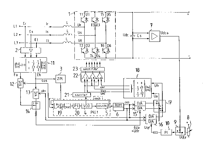
The mains rectifier shown in Figure 1 is connected
to a three-phase mains network L1 - L3 and comprises a
pulse-width modulated (PWM) rectifier bridge 1 consisting
of self-commuting power components, such as transistors T1
- T6, diodes D1 - D6 connected in inverse-parallel with
them, and the filtering components L and Cs connected to
the mains and d.c. sides respectively.
The measured voltages Er, Es and Et of the phases
L1 - L3 of the supplying network are attenuated in an
amplifier unit 2 to a level suited for the regulation
2041~53
electronics. The attenuated voltage signals are passed to
a unit 11 where the real and imaginary components Ea and Eb
of the spatial vector are calculated in a stationary
coordinate system. The calculation is effected using
generally known conversion formulas, shown in the block
representing unit 11 (e.g. Buhler: Einfuhrung in die
Theorie geregelter Drehstromantriebe, Band 1, S. 49-50),
and the summing operational amplifier circuits 14. The
imaginary component Eb is passed to a zero-point indicator
3 which outputs an inverted square wave synchronized with
the voltage in question. This wave is applied to a first
input of the phase comparator 19 of a phase-locked loop
PLL1 consisting of a phase comparator 19, PI-controller 20,
voltage-controlled oscillator (VCo) 4 and a counter 5. The
output of the phase comparator is applied to the input of
the PI-controller 20, whose output determines the output
frequency of the voltage-controlled oscillator (VCO) 4.
The output of the oscillator (VCO) 4 is passed further to
the counter 5, whose output is used as the address of a ROM
unit 6. The ROM unit contains either one or two ROM
circuits holding a pure sine or cosine curve. In the first
alternative, the sine and cosine values are read in
succession, and in the latter (two ROMs) alternative, in
parallel. With the most-significant bit (msb) of the
counter being applied to the second input of the phase
comparator 19, the sine and cosine curves can be
synchronized with the zero point of the imaginary component
Eb of the spatial voltage vector, when the spatial vector
is on the real axis of the calculation coordinates. Thus,
the sine and cosine values obtained from the ROM unit 6 are
also the sine and cosine values of the phase angle of the
spatial voltage vector in the stationary coordinate system.
The real part or d-component Ed of the spatial
voltage vector in the coordinates tied to said vector is
calculated from the real and imaginary components Ea and Eb
of the vector using a generally known conversion equation:
20417~3
.~
Ed = Ea cos ~ + Eb sin ~ (1)
This equation is implemented using two multiplying
D/A converters 12 and 13 and a summing operational
amplifier 14. The procedure is simple and fast and it
reduces the total response time, i.e. the time required for
a change in the mains voltage to produce an effect on the
control of the rectifier bridge 1. In circuit 12, the real
component Ea of the spatial vector obtained from block 11,
is multiplied by the cosine of the new coordinate angle
obtained from the ROM unit 6, and, similarly, in circuit
13 the imaginary component Eb is multiplied by the sine of
the coordinate angle. The summer 14 performs the addition
required by the conversion equation (1). As the new
reference coordinates are oriented in the same direction as
the voltage vector, the voltage vector has no imaginary
part (Eq = 0) in this coordinate system, and its real part
is equal to the absolute value of the indicators of the
phase voltages Er, Es and Et, i.e. the top value of the
phase voltages. This is a way to produce momentary
information on the magnitude of the phase voltages of a
three-phase system.
As will be shown later in connection with Figures
3a and 3b, the effective power absorbed by the rectifier
can be directly influenced by the imaginary part or q-
component of the spatial vector of the rectifier voltagesUr, Us and Ut when a coordinate system tied to the mains
voltage vector is used for reference. In the same way, the
reactive power is influenced by the real part or d-
component of the spatial vector. When it is equal to the
d-component of the mains voltage vector, a system
containing only an ideal mains filter coil L has a power
factor of one.
The d.c. voltage to be regulated is measured by an
attenuating differential amplifier 7, and the measured
voltage Udca thus obtained is compared in a differential
circuit 9 to a voltage Udcr obtained from a setpoint unit
~ 2041753
8. The difference is fed into a controller 10 with a
limited output providing the q-component Uqr of the spatial
vector of the rectified voltages. This component together
with the d-component Udr, which is equal to the d-component
Eda of the mains voltages, unambiguously determines the
direction and magnitude of the spatial vector describing
the rectifier voltages.
After this, the spatial vector corresponding to
the desired rectifier voltages is converted back to
stationary coordinates by means of multiplying D/A
converter units 15 and 16 and a summing unit 17, which
implement the well-known inverted conversion equations:
Ua = Ud cos ~ - Uq sin ~ (2)
Ub = Ud sin ~ - Uq cos ~ (3)
The real and imaginary spatial vector components
thus obtained are further converted in block 18 into three-
phase modulation references Umr, Ums and Umt. The
conversion is effected using summing operational amplifier
circuits implementing the commonly known conversion
equations presented in block 18.
The modulation references Umr, Ums and Umt are
compared by a comparator unit 22 to a triangular wave
obtained from a carrier generator 21, the triangular wave
being synchronized with the voltage-controlled oscillator
(VCO) 4 in the phase-locked loop. This ensures that the
modulation pulse references obtained from the comparator
unit 22 contain no subharmonic components. The modulation
pulse references obtained from the comparator unit 22 are
passed via a base current amplifier unit 23 to the power
components of the mains rectifier, which produce the
desired rectifier voltages Ur, Us and Ut.
Figure 2 illustrates another embodiment of the
control system of the invention. It differs from the
system in Figure 1 as follows:
a) The frequency of the phase-locked loop PLL2 is
controlled by means of the q-component of the spatial
20417~3
voltage vector. It is calculated, like the d-component,
using the other D/A converter in the converter units 12'
and 13' and the summer 14', which implement the well-known
conversion equation:
Eq = -Ea sin ~ - Eb cos ~ (4)
For the calculation coordinate system to be
oriented in the same direction as the spatial voltage
vector, the q-component of the spatial voltage vector
calculated in it must be zero. Thus, the calculated q-
component Eqa is compared to a zero setpoint Eqr in a
differential unit 24. If the differential quantity
obtained from this unit is positive, the PI-controller 20
will increase the frequency of the voltage-controlled
oscillator 4, and vice versa. In this way, the calculation
coordinates are adjusted to orient them in the same
direction with the spatial voltage vector E. In the
procedure, the angle between the spatial vector and the
calculation coordinates is compared continuously, whereas
in the case of the phase-locked loop of Figure 1, this was
only done at the zero point of the voltage Eb.
b) A feed-forward voltage depending on the
differential quantity obtained from the d.c. voltage and
setpoint voltage Udcr, has been added to the formation of
the d-component Udr of the rectifier voltage. If the d.c.
voltage is not equal to the setpoint Udcr, the voltages Ur,
Us and Ut obtained from the rectifier bridge 1 will not
correspond to the modulation references Umr, Ums and Umt.
Therefore, the summer 25 adds to the d-component Eda a
signal proportional to the voltage difference. This signal
is obtained with a scaling circuit 27 and it compensates
the error caused by the voltage difference in the d-
component, which is significant with regard to the reactive
power. The voltage controller 10 effects the correction of
the q-component Uqr.
c) The effect the resistances R of the filter
coils L have on the formation of reactive power is
20417~
.,
eliminated using an additional reference signal of the d-
component Udr, which is proportional to the q-component
Uqr. To this end, the summer 25 adds to the d-component
Eda a signal proportional to the q-component Uqr, obtained
from a scaling circuit 26. Details for this correcting
signal are given in connection with Figures 4c and 4d.
d) The maximum value of the reference value Udr
of the rectifier voltages depends on the magnitude of the
q-component Uqr. As the absolute value of q-component Uqr
increases, the allowed maximum value Udrm of d-component
Udr must be reduced to ensure that the allowed maximum
values of the modulation references, i.e.
Umrh = Umsh = Umth = ~Udrm2 + Uqr2 (5)
formed from them, will never exceed the maximum values of
the triangular wave used for their modulation, and also to
ensure that the whole permitted range of variation of d-
component Udr is continuously in use. This limiting
circuit consists of block 28, which is implemented using
known operational amplifier circuits. In the limiter, the
dependence of the maximum value of d-component Udrm, of q-
component Uqr has been linearized for simplification.
Figures 3a and 3b show the current and voltage
vectors I and _, which are used to clarify the principle of
regulation of the effective and reactive powers of the
system. The known general equations for effective and
reactive power are:
P = 3/2 Re ~EI*} = 3/2 (EdId + EqIq) (6)
Q = 3/2 Im {EI*} = 3/2 (+EdIq - EqId) (7)
If the regulation takes place in a coordinate
system oriented in the same direction as the voltage
vector, the latter term in the component-form equations
disappears (Eq = O). When the magnitude of the mains
voltage vector E = Ed is constant, the effective power P
can be regulated by the d-component Id of the current and
the reactive power Q, by the q-component Iq. In the
regulation system of the invention, the reactive power is
2041753
kept at zero, i.e. the current vector I is adjusted until
it takes the same direction with the voltage vector E.
This means, both in the case of Figure 3a, in which power
flows from the supplying network to the load, and in the
case of Figure 3b, in which power flows from the load to
the supplying network, that the vector jXI of the voltage
across the filter inductance L is perpendicular to the
mains voltage vector E. This condition is satisfied when
the d-component Ud of the vector _ of the rectifier voltage
is equal to the vector of the mains voltage. On the other
hand, in this case, in a stationary condition, the q-
component Uq of _ determines the magnitude of the current
vector I (= Id), and it can be used directly to adjust the
effective power of the system.
Figures 4a - 4d show the current and voltage
vectors in different cases when the resistances of the
filtering coils L are taken into consideration. As can be
seen from Figures 4a and 4b, corresponding to Figures 3a
and 3b, the vector RI of the voltage across the resistances
changes the situation in such a way that the current vector
I no longer runs in the same direction as the voltage
vector E although the d-component Ud = E. To nullify the
reactive power of the system in this case, the magnitude of
the d-component Ud must be changed by an amount equal to
the vector RI, as shown by Figures 4c and 4d. Figure 4c
represents a situation where power is flowing from the
mains to the load, and Figure 4d a situation where power is
flowing from the load to the mains. Since the current
vector I in these cases is determined directly from the
magnitude of the q-component Uq, the d-component Ud must be
altered proportional to the q-component Uq. The
coefficient proportion is determined by the inductance L,
resistance R and the angular frequency of the mains. In
the control system illustrated by Figure 2, this correction
is performed by means of the summer 25 and block 26.
~ 21)417~3
It is obvious to a person skilled in the art that
different embodiments of the invention are not restricted
to the examples described above, but that they may instead
be varied within the scope of the following claims.