Note: Descriptions are shown in the official language in which they were submitted.
2041929
The present invention relates to a connector bank for telecommunication
systems.
A connector bank for telecommunication systems is known in the art from
DE 37 30 662 A1. Therein, the contact elements are formed as solder pins at the
connecting elements. The contact elements penetrate a bottom opening of the plastic
housing of the connector bank, and are soldered in respective boreholes of a printed-
circuit board to enable electrical connection of the connecting elements to the circuit
tracks of the printed-circuit board. Each terminal position of a connector bank may,
during an operational period of many years, be connected and disconnected up to 200
times. When connecting cable wires to the connecting elements, the contact elements
of which are soldered in boreholes of the printed-circuit board, high connect forces will
occur when the wires are pressed into the cutting/clamping contact slots of the
connecting elements. When disconnecting cable wires from the connecting elements,
there are correspondingly lower disconnect forces. Due to manufacturing tolerances,
the connecting elements can often move within the housing of the connector bank. As
a result of this movement, the contact elements are not always supported on the
housing during connection and disconnection. In this case, all connect and disconnect
forces act directly on the solder joint between the contact element and the printed-
circuit board. When connect and disconnect forces are too high, any of the solder joint,
the printed-circuit board, orthe circuit tracks on the printed-circuit board nearthe solder
joint can be damaged. A consequence of this damage in the region of the solder joint
is electrical contact interruptions due to fine cracks and/or possible destruction of the
solder joint.
It is therefore an object of the present invention to provide a connector
bank for telecommunication systems, in which there is no risk of contact interruption
between the contact element and the circuit track even after multiple connections and
disconnections of cable wires at the associated connecting elements.
The connector block for telecommunication systems is provided,
according to an aspect of the invention, as comprising: a housing; a plurality of
connecting elements disposed within said housing, each connecting element being
formed of flat, electrically conductive material, and including cutting/clamping members
for receiving and electrically connecting to a respective cable wire; and a plurality of
contact elements disposed within said housing, for establishing an electrical connection
between respective ones of said connecting elements and circuit tracks of a printed-
-~L
20~19~9
circuit board, each said contact element comprising a contact pin, and a fork-shaped
contact member capable of surrounding a respective connecting element and
maintaining sliding electrical contact therewith.
Another aspect of the present invention provides a connector bank
between a wire and a circuit board, the connector comprising: a connecting element
formed of flat sheet metal and having cutting/clamping members on one end, said
cutting/clamping members defining a slot for receiving the wire, said slot having edges
for making electrical contact with the wire, said cutting/clamping members being forced
apart during said electrical contact and applying said force to said connecting element,
said connecting element extending downwardly toward the circuit board and receiving
said force from said cutting/clamping members during said electrical contact; contact
means for forming an electrical connection to the circuit board, said contact means
having a plug connector means forming an electrical connection between said contact
means and said connecting element, said plug connector means having a contact
range allowing relative movement between said contact means and said connecting
element thereby preventing said force applied to said connecting element from reaching
said contact means; said plug connector means forming a fork-type contact surrounding
a portion of said flat sheet metal for sliding contact upon said application of said force
to separate said cutting/clamping members; and a housing securely holding said
connecting element, said housing being fastened to the circuit board and absorbing
said for supply to said connecting element by said cutting/clamping members.
By providing the contact elements as separate components, there is no
direct, load carrying connection between the connecting elements and the contactelements. Each contact element is instead connected with its associated connecting
element through a plug connector member which is in turn attached to a respective
contact pin. With this arrangement, when connecting cable wires to the connecting
elements, the connection force cannot be transferred from the connecting element to
the plug connector member, as the plug connector element is movable relative to the
connecting element. This in turn prevents the connection force from being transferred
to the contact pin of the contact element, thereby eliminating the risk of damaging the
solder joint when connecting cable wires to the connecting elements. Similar
considerations apply for the disconnect procedure.
2041929
In a preferred embodiment, the plug connector element, for connecting
elements made from flat electrically conductive material such as steel, is formed as a
fork-type contact, which is slidably displaceable on a flat section of the connecting
element. For limiting the penetration depth of the contact element in the housing, a set
of plug shoulders are disposed on the periphery of the contact element between the
contact pin and the plug connector member.
In the following, the invention is described in more detail based on three
different exemplary embodiments of connector banks for telecommunication systems,
reference being made to the appended drawings in which:
Figure 1 illustrates a cross-section through a connector bank with
connecting contacts according to a first embodiment of the invention;
Figure 2 illustrates a cross-section through a connector bank with
disconnecting contacts according to a second embodiment the invention;
Figure 3 illustrates a cross-section through a connector bank with
switching contacts according to a third embodiment the invention;
Figure 4 illustrates a side view of a connector bank according to the
invention;
Figure 5 illustrates a bottom view of a connector bank according to the
invention; and
Figure 6 shows a view of the contact element of the invention.
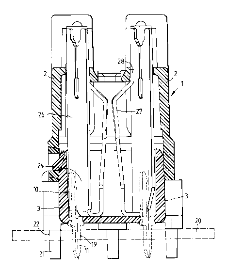
Referring to Figure 1, a first embodiment of the connector bank
according to the invention comprises a plastic housing 1 which consists of an upper
housing section 2 and a lower housing section 3, which are snap-fitted together.Disposed within the plastic housing 1 are connecting elements 4 of flat electrically
conductive material. The connecting elements 4 are composed of two cutting/clamping
connecting elements 5, which may be connected from above with cable wires, and acentre contact 6 connected to the cutting/clamping connecting elements 5 via a
crosspiece 7 located at the bottom of the lower housing section 3. The two
cutting/clamping connecting elements 5 are arranged parallel to each other at an angle
of 45~ relative to the longitudinal axis of the plastic body 1, so that they are bent by
45 off the drawing plane shown in Figure 1.
20419~9
In the bottom 8 of the lower housing section 3 are disposed slots 9 in
two parallel rows, as shown in Figure 5. The slots 9 are grouped into pairs of opposed
slots, each pair belonging to one cutting/clamping connecting element 5. Contactelements 10 (see Figure 6) may be inserted into the slots 9 from the underside of the
plastic housing 1. As illustrated, the contact element 10 forms a separate component
composed of a contact pin 11 and a plug connector element 12. As illustrated in Figure
6, the contact elements 10 have a forked-shape with two resilient arms 13,14 which are
bevelled towards each other at their free ends and provided with contact lugs 15.
Between the contact pin 11 and the plug connector element 12 are disposed two pairs
of plug shoulders 16,17, which engage with the bottom 8 of the lower plastic housing
3, and serve to fix the contact element 10 in position.
As shown in Figure 1, contact elements 10 are inserted through
respective slots 9, towards the interior of the housing 1, until the plug shoulders 16,17
engage with the bottom 8 of the lower plastic housing 3 and clamp the contact element
10 to the bottom 8. To facilitate insertion and clamping, the upper plug shoulders 17,
disposed near the resilient fork arms 13,14 are shorter than the plug shoulders 16
disposed near the contact pin 11. The fork slot 18 surrounds the lateral section of the
flat crosspiece 7 of the connecting element 4 so that the contact lugs 15 form an
electrical contact connection with the connecting element 4.
Once installed, the contact pins 11 project downwardly from the plastic
housing 1 so as to serve as solder pins which may be fitted into a respective borehole
19 assigned to a respective circuit track of a printed-circuit board 20 onto which the
connector bank 1 is attached.
The lower housing section 3 of the plastic housing 1 comprises two
additional plastic pins 21 which penetrate respective boreholes 22 of the printed-circuit
board 20. The connector bank may subsequently be rigidly riveted onto the printed-
circuit board 20 by hot-forming the pins 21.
In a second embodiment of the connector bank shown in Figure 2,
disconnecting elements 25 are provided in place of the connecting elements 4
described in the first embodiment. The disconnecting elements 25 comprise central
disconnect contact lugs 23 which permit disconnection of the two elements 25 by the
insertion of an electrically insulating separator element (not shown) between the central
disconnect contact lugs 23.
5 20~19~9
In a third embodiment of the connector bank shown in Figure 3,
switching elements 26 are provided in place of the connecting elements 4 described
in the first embodiment. The switching elements 26 comprise central connecting
positions 27 which are held spaced by bent-off portions 28 resting against the inner
surfaces of the housing. With this arrangement, the two switching elements 26 may
be electrically connected together by inserting an electrically conducting connecting
plug (not shown) between the central connecting positions 27.
In both of the second and third embodiments, the foot section 24 of the
disconnecting or switching elements (25, 26 respectively) has a flat section, whereon
the fork-type contact 12 of the contact elements 10 can be plugged. After assembly
of a connector bank provided with either connecting elements 4, disconnecting
elements 25, or switching elements 26, the contact elements 10 can optionally beinserted through slots 9 of the plastic housing 1. Thus, it is not necessary to modify
any of the connecting elements 4, disconnecting elements 25 or switching elements 26
in order to accommodate installation of contact elements 10. Furthermore, a connector
bank can be constructed having elements (4,25 or 26) of only one type, or alternatively
having two or more different types of elements.
Thus it will be apparent to those skilled in the art that there are many
ways in which the connector bank of the invention may be varied without departing from
the scope of the appended claims.