Note: Descriptions are shown in the official language in which they were submitted.
CA 02042171 2001-08-03
HIGH-SPEED PACKET SWITCHING APPARATUS AND METHOD
Reference to Related Applications
This application is related to U.S. Patent 5,055,999
issued October 8, 1991 for the invention entitled
"Multiprocessor Digital Data Processing System", assigned
to the assignee hereof.
This application is also related to U.S. Patent
5,119,481 issued June 2, 1992 for the invention entitled
"Interconnection System for Multiprocessor Structure",
assigned to the assignee hereof.
This application is also related to Canadian patent
application serial number 2,019,299 for the invention
entitled "Multiprocessor System with Multiple Instruction
Sources", assigned to the assignee hereof.
This application is also related to U.S. Patent
5,297,265 issued March 22, 1994 for the invention entitled
"Shared Memory Multiprocessor System and Method of
Operation Thereof" and U.S. Patent 5,251,308 which issued
October 5, 1993 for the invention entitled "Shared Memory
Multiprocessor with Data Hiding and Post-Store"
CA 02042171 2001-08-03
2
Background of the Invention
This invention relates generally to systems for
packet switched communications networks, and, more
particularly, relates to apparatus and methods utilizing a
high-speed, multiprocessor packet switching configuration.
A wide range of telecommunications network
configurations have been proposed or implemented in recent
years for providing communication between data handling or
data communications devices. In particular, packet
switching systems were developed to fulfill a demand for
low cost data communications in networks that provide
access to host computers.
In conventional packet switched systems, digital data
cells or packets are transmitted to a selected destination
by a terminal, computer, applications program or other
data handling device. The destination can be another data
handling or data communication apparatus or system. In
many packet switched systems, special-purpose computers
are employed as packet switching processors -- i.e.,
~~~~~e~
-3-
communication processors adapted to direct packets
along the network.
One class of packet switching systems
utilizes predetermined paths through the network, in
which packets generated by a plurality of users share
link and switch facilities as the packets travel over
the network. In these systems, the packets must be
stored at nodes between transmission links until the
packets can be forwarded along the appropriate
destination link. This class of data transmission
system is referred to as virtual circuit or
connection-oriented transmission.
Another class of packet switching systems
utilizes connectionless transmission, which requires
no initial connection for a data path through the
network. In these systems, individual data cells or
packets, including a destination address, are routed
through the network from source to destination via
intermediate nodes.
The virtual circuit system is utilized in a
public network established by Telenet Communications
Corporation. This system employs a two-level
hierarchy to route data packets. One level of the
hierarchy is a network having a plurality of hubs and
nodes, each of which utilizes a cluster of switches.
The second level includes smaller area networks
having trunks, access lines and clustered lower level
switches connected to each hub. The Telenet system
utilizes the X.75 protocol promulgated by the
International Telegraph and Telephone Consultative
~;~~~'.'~1
-4-
Committee of the International Telecommunications
Union (CCITT) as an interface for connecting
computers to a packet-switched network. The protocol
is structured in a three-layered configuration, and
the layers are referred to as the physical level, the
frame level, and the packet level. Routing paths in
the Telenet system are determined by a packet
switching processor, which utilizes routing tables
indicating available links from each hub. The
conventional packet switching processor used in the
Telenet system includes a main memory unit, line
processors that control access to user lines, and a
central processing unit (CPU) that controls routing
at the packet level. The CPU employs a table of
trunk-to-trunk active virtual circuits to identify
appropriate hubs and virtual circuits for connecting
access-requesting users. In the Telenet system, each
user transmitting data across the network must first
write its data packets into main memory, via a bus.
The line processors associated with each user compete
fox access to the bus, in accordance with a
conventional token-passing configuration under the
control of an arbitration unit.
Another form of conventional virtual circuit
packet switching system utilizes multiple bus request
chains having different predetermined priorities.
Each chain in the system employs an arbitration
scheme similar to that described above.
In yet another euample of a conventional
packet switching network, a user seeking access to
the bus must first transmit a selected signal pattern
-5-
onto the arbitration bus. Several line units can
drive the bus simultaneously in this configuration.
The driving line units periodically read these signal
patterns and, based on the priorities of other
requesters, determine whether to maintain or abandon
their respective requests. This process continues
unit an arbitration unit declares a winner.
Conventional packet switching systems,
however, suffer significant limitations in
communications bandwidth and speed, resulting from
their bus arbitration schemes and the requirement of
writing packets into main memory across a
bandwidth-limited bus.
For example, in systems utilizing
token-passing arbitration, a requesting unit must
maintain its request and remain idle until the token
is passed along the chain to that unit, even if that
unit is the only processor requesting access to the
bus. Time and communications channel capacity are
squandered while the token is passed from user to
user. As a result, certain conventional systems of
this type are limited to a data transmission rate no
greater than approximately 164 megabits/second.
One object of the invention, therefore, is
to provide improved packet switching methods and
apparatus enabling enhanced packet transmission rates.
Another object of the invention is to
provide packet switching methods and apparatus that
afford high bandwidth packet transfer.
A further object of the invention is to
provide packet switching methods and apparatus
enabling multiple requesting processors to receive
substantially instantaneous access to the packet
switched network.
Another object of the invention is to
provide such methods and apparatus capable of
handling a wide range of existing and proposed packet
protocols.
Still another object of the invention is to
provide packet switching methods and apparatus that
enable substantially simultaneous handling of packet
switching operations and applications program
processes.
Other general and specific objects of the
invention will in part be obvious and will in part
appear hereinafter.
summary of the Invention
The foregoing objects are attained by the
invention, which provides digital packet switching
methods and apparatus for selectively switching
P
digital signal packets between a set of nodes. The
invention includes multiple processing cells, each
having a processor coupled to an associated
content-addressable memory element. Packet
processors, electrically coupled to the memory
elements, selectively receive packets from the nodes
and transmit the packets into at least one of the
-
plural memory elements; or receive packets from the
memory elements and transmit the packets to at least
one of the nodes.
One aspect of the invention includes memory
management elements, coupled to the memory elements,
for accessing one or more of the
information-representative signals stored in the
plural memory elements. The in-cell processors can
include access request elements for requesting access
to an information-representative signal. The access
request elements can also generate an
ownership-request signal to request priority access
to an information-representative signal.
In another aspect of the invention, the
memory element associated with the requesting
processor includes control elements for selectively
transmitting the access-request signal to the memory
management element. The memory management elements
can also include memory coherence elements. These
coherence elements respond to certain
ownership-request signals by exclusively allocating
physical storage space in the memory element
associated with the requesting processor and storing
the requested information-representative signal
therein.
A further aspect of the invention includes a
plurality of information transfer domains, including
a first domain having a plurality of domain(0)
segments. Each domain(0) segment includes an
associated bus element and a first plurality of
_g_
processing cells connected to the bus element for
transferring information-representative signals.
Each cell has a central processor and an associated
content-addressable memory element for storing
information-representative signals. The memory
elements, in turn, include interface elements
connected with the associated central processor and
with the bus element fox transferring
information-representative signals. The cells are
arranged so that the transfer of
information-representative signals between the
associated central processors takes place only
through the respective memory element.
This aspect of the invention further
includes a domain(1) segment having an associated bus
element and a plurality of routing elements. Each
routing element is connected to the bus element
associated with the domain(1) segment and to the bus
element associated with one of the domain(0)
segments, for transferring information-representative
signals between the domain(1) segment and the
associated domain(0) segment. The processing cells
associated with each of the domain(0) segments can
transfer signals with the processing cells associated
with the remainder of the domain(0) segments only
through the domain(1) segment.
In a further aspect of the invention, the
interconnected processors described above include a
first processor, coupled to at least one
content-addressable memory element, for normally
processing an instruction stream including
_g_
instructions from a first instruction source; and at
least one of the other processors includes a packet
processor for bidirectional packet transfer between
the nodes and the memory elements. The packet
processors include insert elements for inserting one
or more inserted-instructions to be processed by the
first processor in the same manner as, and without
affecting processing sequence of, the instructions
from the first instruction source.
In another aspect of the invention, at least
one of the memory elements includes a data subpage
containing one or more information-representative
signals and forming at least part of a data page. At
least one of the central processors includes access
request elements for generating an access-request
signal to request access to a data subpage stored in
the memory elements. In accord with this aspect of
the invention, the memory management element responds
to certain access-request signals by allocating,
within the memory element associated with the
requesting central processor, physical storage space
for the data page associated with the requested data
subpage, and storing the requested data subpage
therein. The memory management elements further
include de-allocation elements for de-allocating
physical storage space allocated to a selected data
page in the memory elements. This de-allocation is
effected prior to, or substantially concurrent with,
the allocation of the physical storage space for the
data page associated with the requested data subpage.
10
A further aspect of the invention includes
the multiple domain configuration described above, as
well as a selected first processor for normally
processing an instruction stream containing
instructions from a first instruction source. In
accord with this aspect of the invention, at least
one of the other interconnected processors includes a
packet processor for bidirectional packet transfer
between the nodes and the memory elements. This
packet processor includes insert elements for
inserting one or more inserted-instructions to be ..,
processed by the first processor in the same manner
as, and without affecting processing sequence of, the
instructions from the first instruction source.
Yet another aspect of the invention includes
at least one remote processing cell, each remote
processing cell including a central processor coupled
for information transfer with an associated memory
element. A remote interface module coupled to the
remote cell transfers information-representative
signals between the memory element associated with
the remote processing cell and the memory elements
associated with other processing cells. The remote
c~:ll can reside at a point physically remote from
other cells, and the interface module can include
elements for transmitting the information-
representative signal between the physically remote
point and other cells. More particularly, the remote
interface module can include fiber optic transmission
media for carrying information-representative signals
between the remote cell and the other cells.
m
_11_ ~~~~~ 9
In accord with one aspect of the invention,
the packet processors include packet receive
elements, in electrical communication with at least
one of the nodes, for receiving the digital signal
packets from the nodes; and packet splitter elements,
in electrical communication with the receive
elements, for splitting each digital signal packet
received from the nodes into a header portion and a
data portion.
The packet processors also include packet
receive buffer elements, containing a buffer element
in electrical communication with the packet splitter
elements, for storing the digital signal packets
split by the packet splitter elements. The packet
processors further include frame processing elements,
in electrical communication with the packet receive
buffer elements and the memory elements. These frame
processors retrieve the digital signal packets from
the packet receive buffer elements, execute selected
processing on the digital signal packets, and
transmit the digital signal packets to the plurality
of memory elements. The packet processors further
include error checking elements for checking the
received digital signal packets for errors, and for
storing the results of the checking operation with
the header portions of the received digital signal
packets.
In another aspect of the invention, the
cells include receive queue elements for storing in
the memory elements at least one receive queue. The
receive queue includes a data structure containing
-12-
digital signal packets received from the packet
processors. Any of the processing cells can retrieve
selected packets from the receive queue for
processing. The cells also have transmit queue
elements for storing at least one transmit queue in
the memory elements. The transmit queue, which
corresponds to at least one of the nodes, comprises a
data structure containing digital signal packets to
be transmitted to at least a selected one of the
nodes.
The cells also comprise receive queue packet
transfer elements, in communication with the receive
queue elements and the transmit queue elements, for
selectively transferring selected digital signal
packets from the receive queues to at least a
selected transmit queue, responsive to control
signals generated by the plurality of processors.
Further in accord with this aspect of the
invention, the frame processors contain elements for
loading selected ones of the digital signal packets
into the receive queues. The frame processors can
also contain direct packet transfer elements, in
electrical communication with the packet receive
buffer elements, and responsive to the header portion
of the digital signal packets, for transferring
selected digital signal packets from the packet
receive buffer elements to the transmit queue. The
framelprocessors also include units coupled to the
transmit queue elements for retrieving packets from
the transmit queue, responsive to the header portion
of the digital signal packets. These packets are
CA 02042171 2001-08-03
- 13 -
stored in packet transmit buffer elements, and
subsequently transmitted to selected nodes by packet
transmit elements.
A further aspect of the invention provides
application service queue elements in at least one
processing cell, for storing an application service queue.
This queue includes a data structure containing packets to
be serviced by the processing cells in accordance With at
least one application program. Packets can be loaded from
the receive queues into the application service queue, in
response to control signals generated by the processors in
accordance with the application programs.
Application completion queue elements are
provided for storing an application completion queue.
This queue includes a data structure containing packets
generated by the processing cells in accordance with the
application program. Transfer elements are provided for
loading selected packets from the application completion
queue into the transmit queue
The invention will next be described in
connection with certain illustrated embodiments; however,
it should be clear to those skilled in the art that
various modifications, additions and subtractions can l~,e
made without departing from the spirit or scope of the
claims.
In a further aspect, the present invention
provides a digital packet switching apparatus for
selectively switching digital signal packets between a set
of nodes, said digital signal packets being configured in
accordance with a selected protocol, the apparatus
comprising, A. plural processing cells, each being
CA 02042171 2001-08-03
- 13a -
associated with at least one of said nodes, and each
including a processing unit coupled to an associated
memory element for storing information-representative
signals, including digital signal packets, or portions
thereof, packet processing means, coupled to at least one
of the nodes associated with that processing cell and to
at least the memory element of that processing cell, for
at least one of (i) receiving a digital signal packet from
that node and transmitting at least a portion of that
digital signal packet for storage in that memory element,
or (ii) receiving at least a portion of a digital signal
packet from that memory element and transmitting a digital
signal packet, including at least that portion, to that
node, B. memory management means coupled to the memory
elements of said plural processing cells for accessing one
or more of said information-representative signals stored
therein, C. at least a requesting one of said processing
units including access request means for generating an
access-request signal representative of a request for
access to an information-representative signal stored in
any of said memory elements, said access request means
including means for selectively generating said access-
request signal to include an ownership-request signal
representative of a request for priority access to the
requested information-representative signal, wherein said
requested information-representative signal can comprise a
digital signal packet, or portion thereof, at least the
memory element associated with the requesting processing
unit including control means for selectively transmitting
said access-request signal to said memory management
means, D. said memory management means including memory
coherence means responsive to selected ones of said
ownership-request signals for allocating, only within the
memory element associated with the requesting processing
unit, physical storage space for the requested
CA 02042171 2001-08-03
- 13b -
information-representative signal, Wherein that space is
the exclusive storage space for the requested information-
representative signal with respect to all of said memory
elements, and for storing that requested information-
representative signal in that exclusive physical storage
space.
In a still further aspect, the present invention
provides a digital packet switching apparatus for
selectively switching digital signal packets between a set
of nodes, said digital signal packets being configured in
accordance with a selected protocol, the apparatus
comprising, A. a plurality of information transfer domains
each including one or more segments, said plurality of
information transfer domains including a first information
transfer domain having a plurality of domain(O) segments,
each including an associated bus element and a first
plurality of processing cells connected to said bus
element for transferring information-representative
signals therebetween, B. each of said processing cells
being associated With at least one of said nodes, and
including a processing unit and an associated memory
element for storing information-representative signals,
said information-representative signals, including digital
signal packets, or portions thereof, means for identifying
each said information-representative signal stored in tie
associated memory with a corresponding SVA identifier,
packet processing means, coupled to at least one of the
nodes associated with that processing cell and to at least
the memory element of that processing cell, for at least
one of (i) receiving a digital signal packet from that
node and transmitting at least a portion of that digital
signal packet for storage in that memory element, or (ii)
receiving at least a portion of a digital signal packet
from that memory element and transmitting a digital signal
CA 02042171 2001-08-03
- 13c -
packet, including at least that portion, to that node, C.
at least a requesting one of said processing units
including means for generating an access-request signal
representative of a request for access to an information-
representative signal stored in a memory element of any
other of said processing cells, wherein said requested
information-representative signal can comprise a digital
signal packet, or portion thereof, and said access-request
signal including an identifier component representative of
the SVA identifier of the requested information-
representative signal, said requesting processing cell
including means for transmitting that access-request
signal on the associated domain(0) bus element, D. said
plurality of information transfer domains further
including a second information transfer domain having a
domain(1) segment comprising an associated bus element and
a plurality of routing elements, each said routing element
being connected to the bus element associated with the
domain(1) segment and to the bus element associated with
one of said domain(0) segments for transferring signals
therebetween, and E. each said routing element including
directory means for storing SVA identifier signals of
information-representative signals stored in memory
elements of the processing cells of the associated
domain(0) segment, and further including means for
receiving an access-request signal transferred along any
one of the bus element of the domain(1) segment and the
bus element of the associated domain(0) segment for
selectively transmitting that access-request signal along
the bus element associated with the other of those bus
elements based on a comparison of the identifier component
of that access-request signal with said SVA identifier
signals in said directory element.
CA 02042171 2001-08-03
- 13d -
In a further aspect, the present invention
provides A method of operating a digital packet switching
apparatus for selectively switching digital signal packets
between a set of nodes, said digital signal packets being
configured in accordance With a selected protocol, said
method including the steps of, A. providing plural
processing cells, each being associated with at least one
of said nodes and each including a processing unit coupled
to an associated memory element for storing information-
representative signals, including digital signal packe~s,
or portions thereof, B. selectively executing, within at
least one of said processing cells, any of (i) receiving a
digital signal packet from a node associated with that
processing cell and transmitting at least a portion of
that digital signal packet for storage in the memory
element of that processing cell, or (ii) receiving at
least a portion of a digital signal packet from the memory
element of that processing cell and transmitting a digital
signal packet, including at least that portion, to at
least one of said nodes associated With that cell, C.
generating within a requesting one of said processing
units an ownership-request signal representative of a
request for priority access to an information-
representative signal stored in the memory element of any
of said processing cells, wherein said requested
information-representative signal can comprise a digital
signal packet, or portion thereof, D. determining whether
the requested information-representative signal is stored
Within a memory element other than one associated with the
requesting processing unit, and responding to a
determination that the requested information-
representative signal is stored in a memory element other
than the one associated with the requesting processing
unit for allocating, only within the memory element
associated with the requesting processing unit, physical
i
CA 02042171 2002-04-18
- 13e -
storage space for the requested information-representative
signal, wherein that space is the exclusive physical
storage space for the requested information-representative
signal with respect to all of said memory elements, and
storing the requested information-representative signal in
that exclusive physical storage space.
In a still further aspect, the present invention
provides a digital packet switching apparatus for
selectively switching digital signal packets between a set
of nodes, said digital signal packets being configured in
accordance with a selected protocol, the apparatus
comprising plural processing cells, each including a
central processing unit coupled to an associated memory
element of plural memory elements, at least one of said
plural memory elements including a data subpage comprising
one or more information-representative signals and forming
at least part of a data page, at least one of said central
processing units including access request means for
generating an access-request signal representative of a
request for access to a data subpage stored in one or more
of said memory elements, memory management means, coupled
to said processing cells, responsive to at least selected
ones of said access-request signals for allocating, within
the memory element associated with the requesting central
processing unit, physical storage space for the data page
associated with the requested data subpage, and for
storing the requested data subpage therein, said memory
management means further including de-allocation means for
de-allocating physical storage space allocated to a
selected data page in one or more of said memory elements,
said de-allocation being effected prior to, or
substantially concurrent with, the allocation of said
physical storage space for the data page associated with
the requested data subpage, and packet processing means,
electrically coupled to at least one of said plural memory
CA 02042171 2002-04-18
- 13f -
elements, for selectively executing any of (i) receiving
at least one digital signal packet from at least one of
said nodes and transmitting said at least one digital
signal packet into at least one of said plural memory
elements, or (ii) receiving at least one digital signal
packet from at least one of said plural memory elements
and transmitting said at least one digital signal packet
to at least one of said nodes.
-14-
Brief Description of the Drawings
For a fuller understanding of the nature and
objects of the invention, reference should be made to
the following detailed description and the
accompanying drawings, in which:
FIG. 1 is a schematic diagram depicting a
packet switching network configuration constructed in
accord with the invention;
FIG. 2 is a schematic diagram depicting
conventional OSI layered communications architecture;
FIG. 3 is a schematic diagram depicting a
multiprocessor structure employed in the packet
switching system of FIG. 2;
FIG. 4 depicts an exemplary processing cell
in the multiprocessor structure of FIG. 3;
FIGS. 5A-5C depict further embodiments of a
processing cell constructed in accordance with the
invention;
FIGS. 5D and 5E show detail of processing
cells containing packet processing units (PSUs) in
accord with the invention;
FIG. 6 depicts packet flow in the system of
FIG. 2;
_15- ,~4' ~4~~'~
FIG. 7 provides detail of the PSUs of FIGS.
5D and 5E;
FIG. 8 depicts packet transfer to the
receive queue in the PSU of FIG. 7;
FIG. 9 shows packet transfer to the transmit
queue; and
FIG. 10 depicts transfer of packets from the
transmit queue to the transmit FIFO buffer.
Description of Illustrated Embodiments
Overview
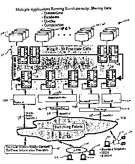
FIG. 1 depicts a packet switching system 100
in accordance with the invention. The system 100
selectively interconnects a plurality of users,
including data handling devices 110 linked by a local
area network (LAN), telecommunications devices 112,
and applications programs operating on 101.1, 101.2,
..., lOl.N. System users can also include other
information providers and inter-exchange carriers
115. The system includes a multiprocessor packet
switching apparatus 10 having a plurality of
processing cells 18, for controlling the operation of
the packet switching system 100 in a manner described
below.
The users shown in FIG. 1 communicate with
the multiprocessor packet switching apparatus 10 via
a switching fabric or network 116. This switching
-16-
fabric can be conventional in design, and can
include, for example, the hubs and links of a
conventional Telenet switching network. When a user
transmits data, switching fabric 116 processes the
data in a known manner to generate digital signal
packets configured in accordance with conventional
protocols. The packets can be routed along lines 118
to physical interface modules 120. Alternatively,
packets can be routed to a circuit switch 119 prior
to reception by a physical interface module 120. The
physical interface modules 120 processes the received
packets, as discussed below in connection with FIG.
6, and transmits the packets to the processing cells
18 of the packet switching apparatus 10. The
illustrated embodiment includes a frame
multiplexor/de-multiplexor 122 interposed between a
physical interface module 120 and a processing cell
18, for executing further processing of signal
packets, in a manner discussed below.
Packet switching apparatus 10 receives
signal packets generated by the users -- including
applications programs 101 -- and transmits each
packet to selected end-users as described hereinafter
in connection with FIGS. Transmission of packets
from the packet switching apparatus 10 to the users
is accomplished in a manner analogous to that of
packet reception.
A significant feature of the invention is
that the packet switching apparatus 10 depicted in
FIG. 1 can operate in conjunction with the existing
ISO Reference Model for Open Systems Interconnection
CA 02042171 2001-08-03
-17-
(OSI). The ISO Reference Model, shown in FIG. 2, has
become a standard for layered communication
architectures.
A detailed description of the ISO Reference
Model and underlying protocols can be found in
Schwartz, Telecommunication Networks' Protocols
Modeling and Analysis, Addison-Wesley, 1987.
Another significant feature of the invention
is the ability of the packet switching apparatus to
operate in conjunction with the proposed Broadband
Integrated Digital Network (B-ISDN) and Synchronous
Optical Network (SONET) standards. B-ISDN is an
emerging standard for high speed digital
communications .
Two principal approaches promulgated for
multiplexing and switching for B-ISDN are Synchronous
Transfer Mode (STM) and Asynchronous Transfer Mode
(ATM). Synchronous time division multiplexing and
circuit switching technologies are based on STM
principles. Asynchronous time division multiplexing
and high-speed packet switching are based on ATM
principles.
Despite recent advances, circuit switching
technology cannot efficiently carry bursty traffic.
Switching fabric resources are wasted when there is
no information to transfer. High speed packet
switching or AM technique eliminate these
limitations, since bandwidth is dynamically allocated
-18-
based on multiple user demand. Another significant
feature of the invention, therefore, is the ability
to support high speed ATM techniques.
Implicit in the ISO Model and similar
architectures is the recognition that the network
communications problem can be divided into two
components. The first involves the communications
network itself. Data delivered by an end user to a
network must arrive at the destination correctly and
in a timely fashion. The second component of the
communications problem is the necessity of ensuring
that the data ultimately delivered to the end user at
the destination is recognizable and in the proper
form for its correct use.
The OSI Reference Model comprises the seven
layers shown in FIG. 2. The lowermost three layers,
201-203, comprise the network structures and services
that address the first part of the communications
problem. The upper four layers, 204-207, comprise
the components and operations that provide services
to the end users. These layers are thus associated
with the end users, rather than with the networks.
The data link layer 202 and the physical
layer 201 ideally provide an error-free communication
link between two nodes in a network. The function of
the physical layer 201 is to ensure that a bit
entering the physical medium at one end of a link
arrives at the destination end. Using this
underlying bit transport service, the purpose of the
data link protocol -- also referred to as frame level
-19-
protocol -- is to ensure that blocks of data are
transferred without errors across a link. These data
blocks are also referred to as frames.
The objective of the network layer 203, also
known as the packet level, is to route the data
through the network, or through multiple networks if
necessary, from source to destination nodes. This
layer also provides for flow or congestion control,
to prevent network resources such as nodal buffers
and transmission links from filling up, possibly
leading to a deadlock condition. In executing these
functions, the network layer uses the services of the
data link layer below to ensure that a block of data
-- i.e., a packet -- transmitted at one end of a link
along a route through the network arrives at its
destination without error.
These network objectives and packet
switching functions are advantageously provided by
exploiting the multiple cell configuration of the
packet switching apparatus 10 depicted in FIG. 1. In
particular, while the multiprocessor structure 10
shown in FIG. 1 includes only one ring, or domain, of
processing cells, the structure can be expanded to
comprise a plurality of domains, as indicated in FIG.
3.
FIG. 3 depicts a multiprocessor structure 10
that can be utilized in connection with a packet
switching practice of the invention. A structure of
CA 02042171 2001-08-03
-20-
this type is further described in commonly-owned U.S.
Patent 5,055,999 for the invention entitled
"Multiprocessor Digital Data Processing System"
The illustrated multiprocessor structure 10
includes three information transfer domains:
domain(0), domain(1), and domain(2). Each
information transfer domain includes one or more-
domain segments, characterized by a bus element and a
plurality of cell interface elements. Particularly,
domain(0) of the illustrated system 10 includes six
segments, designated 12A, 12B, 12C, 12D, 12E and 12F,
respectively. Similarly, domain(1) includes segments
14A and 14B, while domain(2) includes segment 16.
Each segment of domain(0), i.e., segments
12A, 128, ... 12F, comprises a plurality of
processing cells. For example, as shown in the
illustration, segment 12A includes cells 18A, 18B and
18C; segment 12B includes cells 18D, 18E and 18F; and
so forth. Each of those cells include a central
processing unit and a memory element, interconnected
along an intracellular processor bus (not shown). In
accord with the preferred practice of the invention,
the memory element contained in each cells stores all
control and data signals used by its associated
central processing unit.
As further illustrated, each domain(0)
segment may be characterized as having a bus element
CA 02042171 2002-02-O1
- 21 -
providing a communication pathway for transferring
information-representative signals between the cells of
the segment. Thus, illustrated segment 12A is
characterized by bus 20A, segment 12B by 20B, segment
12C by 20C, and so on. As described in greater detail
in commonly-owned U.S. Patent 5,055,999, information-
representative signals are passed between the cells 18A,
18B and 18C of exemplary segment 12A by way of the
memory elements associated with each of those cells.
Specific interfaces between those memory elements and
the bus 20A are provided by cell interface units 22A,
22B and 22C, as shown. Similar direct communication
pathways are established in segments 128, 12C and 12D
between their respective cells 18D, 18E, ... 18R by cell
interface units 22D, 22E, ... 22R, as illustrated.
As shown in the illustration and noted above,
the remaining information transfer domains, i.e.,
domain(1) and domain(2), each include one or more
corresponding domain segments. The number of segments
in each successive segment being less than the number of
segments in the prior one. Thus, domain(1)'s two
segments 14A and 14B number fewer than domain(0)'s six
12A, 12B ... 12F, while domain(2), having only segment
16, includes the fewest of all. Each of the segments in
domain(1) and domain(2), the "higher" domains, include a
bus element for transferring information-representative
signals within the respective segments. In the
,\
-22'
illustration, domain(1) segments 14A and 14B include
bus elements 24A and 24B, respectively, while
domain(2) segment 16 includes bus element 26.
The segment buses serve to transfer
information between the components elements of each
segment, that is, between the segment's plural domain
routing elements. The routing elements themselves
provide a mechanism for transferring information
between associated segments of successive domains.
Routing elements 28A, 28B and 28C, for example,
provide a means for transferring information to and
from domain(1) segment 14A and each of domain(0)
segments 12A, 12B and 12C, respectively. Similarly,
routing elements 28D, 28E and 28F provide a means for
transferring information to and from domain(1)
segment 14B and each of domain(0) segments 12D, 12E
and 12F, respectively. Further, domain routing
elements 30A and 30B provide an information transfer
pathway between domain(2) segment 16 and domain(1)
segments 14A and 14B, as shown.
The domain routing elements interface their
respective segments via interconnections at the bus
elements. Thus, domain routing element 28A
interfaces bus elements 20A and 24A at cell interface
units 32A and 34A, respectively, while element 28B
interfaces bus elements 20B and 24B at cell interface
units 32B and 34B, respectively, and so forth.
Similarly, routing elements 30A and 30B interface
their respective buses, i.e., 24A, 24B and 26, at
cell interface units 36A, 36B, 38A and 38B, as shown.
-23-
FIG. 3 illustrates further a preferred
mechanism interconnecting remote domains and cells in
a digital data processing system constructed in
accord with the invention. Cell 18R, which resides
at a point physically remote from bus segment 20F,
can be coupled with that bus and its associated cells
(18P and 180) via a fiber optic transmission line,
indicated by a dashed line. A remote interface unit
19 provides a physical interface between the cell
interface 22R and the remote cell 18R. The remote
cell 18R is constructed and operated similarly to the
other illustrated cells and includes a remote
interface unit for coupling the fiber optic link at
its remote end.
In a similar manner, domain segments 12F and
14B can be interconnected via a fiber optic link from
their parent segments. As indicated, the respective
domain routing units 28F and 30B each comprise two
remotely coupled parts. With respect to domain
routing unit 28F, for example, a first part is linked
directly via a standard bus interconnect with cell
interface 34F of segment 14B, while a second part is
linked directly with cell interface unit 32F of
segment 12F. These two parts, which are identically
constructed, are coupled via a fiber optic link,
indicated by a dashed line. As above, a physical
interface between the domain routing unit parts and
the fiber optic media is provided by a remote
interface unit (not shown).
CA 02042171 2001-08-03
-24-
FIG. 4 depicts an embodiment of the
processing cells 18A, 18B, ..., 18R of FIG. 3. The
illustrated processing cell 18A includes a central
processing unit 58 coupled with external device
interface 60, data subcache 62 and instruction
subcache 64 over processor bus 66 and instruction bus
68, respectively. Interface 60, which provides
communications with external devices, e.g., disk
drives, over external device bus, is constructed in a
manner conventional to the art.
Processor 58 can comprise any one of several
commercially available processors, for example, the
Motorola 68000 CPU, adapted to interface subcaches 62
and 64, under control of a subcache co-execution unit
acting through data and address control lines 69A and
69B, in a manner conventional to the art, and further
adapted to execute memory instructions as described
below. The processing cells are further described in
commonly-owned U.S. Patent 5,055,999 for the invention
entitled "Multiprocessor Digital Data Processing
System". Schematics for an embodiment of the
processing cells are set forth in the Appendix D filed
herewith.
Processing cell 18A further includes data
memory units 72A and 72B coupled, via cache control
units 74A and 748, to cache bus 76. Cache control
units 74C and 74D, in turn, provide coupling between
cache bus 76 and processing and data buses 66 and
68. As indicated in FIG. 4, bus 78 provides an
CA 02042171 2001-08-03
- 25 -
interconnection between cache bus 76 and the domain(0) bus
segment 20A associated with the illustrated cell.
Preferred designs for cache control units 74A, 74B, 74C
and 74D are discussed in U.S. Patent 5,055,999 for the
invention entitled "Multiprocessor Digital Data Processing
System," and U.S. Patent 5,251,308 for the_invention
entitled "Shared Memory Multiprocessor with Data Hiding
and Post-Store".
In a preferred embodiment, data caches 72A and 72B
include dynamic random access memory (DRAM) devices, each
capable of storing up to 16 Mbytes of data. The subcaches
62 and 64 are static random access memory (SRAM) devices,
the former capable of storing up to 256k bytes of data,
the latter of up to 256k bytes of instruction information.
As illustrated, cache and processor buses 76 and 64
provide 64-bit transmission pathways, while instruction
bus 68 provides a 64-bit transmission pathway. A
preferred construction of cache bus 76 is provided in U.S.
Patent 5,055,999 for the invention entitled
"Multiprocessor Digital Data Processing System". _
CA 02042171 2001-08-03
- 26 -
Those skilled in the art will understand that
illustrated CPU 58 can represent a conventional central
processing unit and, more generally, any device capable of
issuing memory requests, e.g., an I/O controller or other
special purpose processing element.
The instruction execution of a processing cell her-ein
described differs from conventional digital processing
systems in several significant ways. The processing cell
--e. g., 18A-- has multiple processing cells or functional
units --e.g., 58, 60-- that can execute instructions in
parallel. Additionally, the functional units are
"pipelined," to permit multiple instructions to be in
progress at the same time by overlapping their execution.
This pipelining is further described in U.S. Patent
5,055,999 for the invention entitled "Multiprocessor Digital
Data Processing System". Further description of the
instructions discussed herein --including LOADS, STORES,
MOVOUT, MOVB, FDIV and others-- can be found in U.S. Patent
5,297,265 for the invention entitled "Shared Memory
Multiprocessor System and Method of Operation Thereof"._
A processing cell constructed in accordance with the
invention executes a sequence of instructions fetched from
memory. The context of execution can be partially defined
by the architecture, and partially defined by software. The
CA 02042171 2001-08-03
-27-
architectural portion of the execution context can
consist of a context address space, a privilege
level, general registers, and a set of program
counters. The context address space and privilege
level determine what data in the memory system the
instruction stream may reference. General registers,
constructed in accordance with known engineering
practice, are used for computation. These features
are further described in U.S. Patent 5,055,999. The
program counters define what portion of the instruction
stream has already executed and what will be executed
next, as described in greater detail hereinafter.
Two time units can be employed in specifying
the timing of instructions. These units are referred
to herein as "clocks" and "cycles," respectively. A
clock is a unit of real-time which has duration
defined by the system hardware. The processor
performs an instruction fetch every cycle. A cycle
takes one clock unless a "STALL" occurs, in which
case a cycle takes some larger integral number of
clocks. The execution of instructions is described
in terms of cycles and is data-independent.
Pipeline STALLs can result from subcache and
cache management overhead. Most LOAD and STORE
operations will complete without a STALL; however,
any LOAD, STORE, or memory control instruction may
cause a STALL in order to allow the system to
retrieve data from the local cache or from a remote
-.
-28-
cells. These delays are referred to herein as
STALLs. During a STALL, the execution of other
instructions does not proceed, and no new
instructions are fetched. STALLS are not related to
the instruction itself, but to the proximity of the
related data. STALLS are measured in clocks and each
STALL is an integral number of clocks. Even though a
CEU might STALL while obtaining data from the local
cache, the programming model (expressed in cycles)
remains constant.
As shown in connection with the embodiments
of FIGS. 5A-5C, a processing cell 18.1 in accordance
with the invention can include four processing
elements, also referred to herein as "functional
units": the CEU 58, IPU 84, FPU 82 and XIU 60.
While FIGS. 5A-5C illustrate a processing cell 18.1
having four processing elements, those skilled in the
art will appreciate that the invention can be
practiced in connection with a processing cell having
more or fewer processing elements.
In particular, the CEU (Central Execution
Unit) fetches all instructions, controls data FETCH
and STORE (referred to herein as LOADS and STORES),
controls instruction flow (branches), and does
arithmetic required for address calculations. The
IPU (Integer Processing Unit) executes integer
arithmetic and logical instructions. The FPU
(Floating point Processing Unit) executes floating
point instructions. The XIU (eXternal I/o Unit) is a
co-execution unit which provides the interface to
29
external devices. The XIU performs DMA (Direct
Memory Access operations) and programmed I/O, and
contains timer registers. It executes several
instructions to control programmed I/O. The
structure and operation of the XIU is further
described in the Appendix filed herewith.
Referring again to FIG. 5A, the processing
cell 18.1 thus comprises a set of interconnected
processors 58, 60, 82 and 84, including a CEU 58 for
normally processing an instruction stream including
instructions from the instruction cache 64. The flow
of instructions from the instruction cache 64 is
indicated in FIG. 5A by dashed lines 86.
As depicted in FIG. 5A, at least one of the
processors -- in the illustrated example, FPU 82 and
XIU 60 -- can assert instructions, referred to herein
as "inserted-instructions", which can be executed by
the CEU 58. The flow of inserted-instructions from
FPU 82 to CEU 58 is indicated in FIG. 5A by dashed
lines 88. Analogously, the movement of
inserted-instructions from XIU 60 to CEU 58 is
denoted by dashed lines 90.
Moreover, these inserted-instructions can be
executed by CEU 58 in the same manner as, and Without
affecting execution sequence of, the instructions
from the instruction cache 64. Moreover, as further
explained below, the inserted-instructions can have
the same format as the instructions from the first
instruction source, including a first set of digital
instruction bits for specifying selected address
-30-
signals, and a second set of digital instruction bits
for specifying selected command signals.
Inserted-instructions having this format can include
cache management instructions inserted by the
instruction cache 64 or by the cache control unit 74D
depicted in FIG. 4.
While FIG. 5A depicts an instruction cache
64 as the source of instructions, alternatively, the
source of instructions can be a processor or
execution unit --including, under certain
circumstances, the CEU 58-- adapted for asserting
signals to the instruction cache element to cause
instructions to be transmitted from the instruction
cache element to the CEU 58.
As discussed above, the processing cell 18.1
can include an instruction pipeline, comprising
instruction bus 68, for interconnecting the
processors and for carrying the instructions. The
processors, in turn, can incorporate hardware and
software elements for inserting the
inserted-instructions into the instruction pipeline.
The XIU 60 depicted in FIG. 5A can
incorporate input/output (I/O) modules for handling
signals 70 received from, arid transmitted to,
peripheral devices, also referred to herein as
external devices. These I/O modules can include
direct memory access (DMA) elements, which respond to
selected signals from a peripheral device. to insert
DMA instructions which can be processed by the CEU 58
in the same manner as, and without affecting
-31-
processing sequence of, the instructions from the
first instruction source. These processing sequences
are discussed in greater detail hereinafter. The XIU
60 can also include graphics controller circuits,
constructed in accordance with known engineering
practice, for controlling signals transmitted to a
display device; or conventional text search elements
for searching data structures representative of text.
Alternatively, as illustrated in FIG. 5D,
the XIU of FIGS. 5A-5C can be replaced by a
special-purpose packet co-processor 85, discussed in
greater detail hereinafter. Moreover, as FIG. 5E
indicates, the four processors of FIGS. 5A-5C can be
supplanted by a single packet processor that
implements frame level and selected
performance-critical packet level procedures.
Each processor 58, 60, 82, 84 depicted in
FIGS. 5A and 5B can include registers for storing
digital values representative of data and processor
states, in a manner discussed in greater detail
hereinafter. These registers are shown in FIG. 5C,
along with computational units and other logic
elements utilized in one practice of the invention.
The inserted-instructions discussed above control
movement of data into and out of these registers, and
cause execution of selected logical operations on
values stored in the registers.
CA 02042171 2001-08-03
-32-
Additional description of inserted-
instruction processing is provided in Canadian -
application serial number 2,019,299.
The operation of the packet co-processor 85
will next be described in connection with packet flow
control, as illustrated in FIG. 6.
Packet Flow
In accord with the invention, all data
structures required for packet switching control,
including Receive Queues 601, Transmit Queues 602,
application response queue 610 and application
service queue 612, are resident in the cache memory
units 72 associated with the in-cell processing
units. This feature is indicated in FIG. 6, which
also shows that one or more incoming and outgoing
physical links are associated with each Packet
Switching Co-Execution Unit (PSU) 85. One or more
Receive Queues 601 are associated with each incoming
link and one or more Transmit Queues 602 are
associated with each outgoing link. Memory addresses
are assigned to each queue on a segment basis.
Reception from Physical Interface: The
physical receive interface 120.1 associated with the
PSU 85.1 executes the conventional operations that
constitute the remainder of the physical layer and a
portion of the data link or frame layer illustrated
in FIG. 2. Each frame or cell is received from
CA 02042171 2001-08-03
-33-
physical interface 120.1 and delineated by the PSU
85.1. The packet or cell is then split into header
and data portions, and stored in the PSU receive FIFO
buffer 602. The received packet or cell is error
checked, with the results stored with the header.
Receive Frame Level Processing: Referring
again to FIG. 6, the PSU 85.1 associated with the
physical link completes frame level processing and
stores the received frame or cell into the Receive
Queue 601. As indicated above, at least one cache
memory-resident Receive Queue corresponds to each
physical receive link. The PSU 85.1 utilized
inserted-instruction sequences, discussed above in
connection with FIG. 5A, to directly manipulate the
Receive Queue 601.
Packet Level Processing: Because the Receive
Queue 601 and Transmit Queue 602 data structures are
completely resident in cache memory 72, any processor
within the multiprocessor structure 10 can execute
the packet (network) layer protocol. The packet is
moved from the Receive Queue 601 to the appropriate
Transmit Queue 602 based on memory-resident packet
routing and flow control tables. These tables are
discussed in copending U.S. Patent 5,055,999 for the
invention entitled "Multiprocessor Digital Data
Processing System".
Moreover, because most packets require no
computational resources, in the typical case, the PSU
associated with the physical receive link can
9~ ~ ~~ :~. '6'
directly execute the packet level protocol,
transferring the packet directly from PSU to the
appropriate Transmit Queue, and bypassing the Receive
Queue. This is indicated at block 614 of FIG. 6. If
more complex handling is required, the packet is left
in the Receive Queue for packet processing by any
processor, as indicated by block 614.
Packets can also be routed from a link
Receive Queue 601 to an application service queue 612
for higher level processing. Examples of higher
level processing are transactions, database queues,
or computation, in accordance with an application
program running on the multiprocessor structure 10.
Higher level processing employs the same processor
pool and cache memory as do packet switching
operations. In the illustrated embodiment, packets
generated by higher level processing are placed in a
application completion queue 612. Packet level
processing is performed on application-generated
packets in a manner similar to that applied to
packets from link Receive Queues.
Transmit Frame Level Processing: The PSU
85.2 associated with a physical transmit link
performs frame level processing and moves the frame
or cell into a PSU-resident transmit interface,
including FIFO buffer 618, for transfer to the
physical interface 120.2. One or more cache
memory-resident Transmit Queues correspond to each
physical transmit link. In a manner similar to that
discussed above in connection with received packet
-35-
processing, the transmitting PSU 85.2 uses inserted
instruction sequences to directly manipulate the
Transmit Queue.
Transmission to the Physical Interface: The
PSU physical transmit interface 120.2 executes the
remainder of frame level protocol and a portion of
the operations that compose the physical link layer,
in accordance with conventional ISO Reference Model
practice. Each frame or cell is constructed from the
header and data stored in the PSU transmit FIFO
buffer 618, and the appropriate error checking code
is generated in a known manner.
I5 PSU Structure
Organization: As shown in FIG. 7, the PSU
consists of five major blocks: Transmit Buffer 701,
Receive Buffer 702, Command Buffer Register File 703,
Inserted-Instruction Functional State Machine (FSM)
704, and Instruction Decode Unit 705. This set of
units can be divided into two groups: blocks
associated with the physical interfaces, and blocks
associated with the co-execution unit (CEU) interface
or processor bus described above. In particular, the
Transmit Buffer 701 and Receive Buffer 702
interconnect with the physical interface, and
transfer packets to and from the physical interface.
The Command Buffer Register File 703, Inserted
Instruction State Machine 704 and the Instruction
Decoder 705 are associated with the co-execution unit
interface.
CA 02042171 2001-08-03
-3 6-
Transmit Buffer: The Transmit Buffer
includes a Transmit Data FIFO 710, Transmit Head FIFO
711, Header Formatter 712 and Packet Functional State
Machine 713. The Packet FSM coordinates the
construction of the physical packet frame and cells
within a frame from the contents of the Header FIFO
buffer and Data FIFO buffer. The Header and Data
FIFO are previously loaded from the SVA cache by the
Inserted Instruction State Machine. Further
description of these elements is provided in U.S.
Patent 5,055,999 and Canadian application serial number
2,019,299.
The Header Formatter 712 constructs the
physical header, using conventional processes, based
on the data structure fetched from cache, and
responsive to TRANSMIT commands from the command
buffer 703. The Packet FSM 713 constructs the
outgoing frame or cell, by employing operations known
in the digital processing field, based on the header
contents and in response to TRANSMIT commands from
the command buffer 703. The illustrated embodiment
provides enhanced flexibility in the processing of
packet formats and frame level protocols, by applying
the TRANSMIT command to determine Header Formatter
and Packet FSM operations. The Transmit Huffer also
provides appropriate serialization and control
signals for interfacing to the physical interface, in
accordance with known engineering practice.
-37-
Receive Buffer: The Receive Buffer 702
comprises a Receive Data FIFO 714, Receive Header
FIFO 715, Header Splitter 716 and Packet FSM 717.
The Packet FSM 717 operates in accordance With known
digital signal processing principles to coordinate
the reception and splitting of the packet frame, or
signal cell within a frame, into header and data
portions, for placement into Header FIFO 715 and Data
FIFO 714, respectively. The RECEIVE command from the
command buffer 703 is used by the Packet FSM 717 to
appropriately split the header and data portions of
the frame or cell.
The Header Splitter 716 reformats the header
into the data structure to be stored into SVA cache,
based on the RECEIVE command from the command
buffer. As with the Transmit Buffer, flexibility in
the packet format and frame level protocol is
achieved by having the Header Splitter and Packet FSM
operation controlled by the RECEIVE command. The
Receive Buffer 702 also provides the appropriate
parallelization of packet and control signals for
interfacing to the physical interface.
command Buffer: The Command Buffer 703 is a
multiport PSU-resident memory device that holds
RECEIVE and TRANSMIT commands and provides temporary
on-chip storage for portions of cache memory-resident
data structures. Pointers to active entries of cache
memory-resident queues are separately maintained for
Receive and Transmit Buffers.
-38-
In the illustrated embodiment, the command
buffer comprises three READ ports and two WRITE
ports. Two READ ports are allocated for the current
TRANSMIT command for the Transmit Buffer 701, and for
the current RECEIVE command for the Receive Buffer
702. The first WRITE port allows the Transmit Packet
FSM 713 or Receive Packet FSM 717 to update Command
Buffer status. The third READ port is coupled to the
data bus for storing Command Buffer contents directly
into cache memory. The second WRITE port interfaces
to the data bus for receiving accessed contents of
cache memory and storing data into Command Buffer.
IISM: The Inserted Instruction State Machine
(IISM) 709 generates the instructions required to
store frames or cells from the Receive Buffer 702
into cache memory-based queues. The IISM 704 also
generates the instructions required to load frames or
cells from cache memory-based queues into the
Transmit Buffer.
Additionally, the IISM 704 generates the
instructions required to manipulate the cache
memory-based queue structures. These operations
include updating pointers within queue entries,
generating instructions for atomic update of queue
data structures -- including GET, GETW and RELEASE
commands, generating instructions to PREFETCH queue
entries which will be required in the near future,
and POSTSTORING queue entries for which copies will
be required by other cells in the near future. The
PREFETCH instructions, as well as certain LOAD and
STORE instructions, permit programs to request that
-
their local cache acquired read-only, non-exclusive,
or exclusive state. The PREFETCH SUBPAGE command,
for example, requests that a copy of a subpage be
acquired on the local cache in a specified state.
PREFETCH SUBPAGE specifies whether or not the subpage
should be prefetched into the processor's instruction
or data subcache. A subsequent load for the subpage
blocks until the PREFETCH SUBPAGE has completed.
The POST STORE SUBPAGE or PSTSP instruction
causes the local cache to broadcast a read-only copy
of a subpage through the ring if the subpage state is
Exclusive. Each cell whose cache contains a
descriptor for the page containing the subpage
acquires a read-only copy of the subpage. PSTSP
operates in accordance with the following steps:
1. The processor passes the subpage address
and PSTSP request to the local cache.
2. The local cache issues an OK response to
the processor, and processor execution proceeds.
3. If the subpage state is exclusive and if
the subpage address specified by PSTSP does not match
a pending ring request, then
a. The local cache issues an XCACHE.RO
subcache invalidation request to the
processor if the subpage is subcached. THe
processor responds to the invalidation
request by passing data to the local cache
if the subblocks are modified; and
CA 02042171 2001-08-03
-40-
b. The local cache broadcasts a
re~3-only copy of the subpage on the ring.
4. Otherwise, the PSTSP is not executed.
The PSTSP instruction initiates a duplicate
packet process. Duplicate data packets are forwarded
from the originating RING:O based on DUPLIMIT. If
DUP:CONDFORWARD applies, duplicate packets are
conditionally forwarded by RRC:O to Ring:l, if the
page is not exclusively owned by the local Ring: O.
If DUP:ALLFORWARD applies, duplicate packets are
always forwarded by RRC:O to Ring: 1. Ring:l
duplicate data packets are copied by a remote RRC:1
when it has a descriptor allocated for the
corresponding page within its local Ring:O and the
Extract Buffer is in the EXTBUF:ALL region.
These commands, including PREFETCH and
pOSTSTORE, are described in greater detail in U.S.
Patent 5,055,999 and U.S. Patent 5,251,308.
Instruction Decode- The Instruction Decode
block 705 decodes instructions to be executed by the
PSU, and enables the PSU 85 to track the instruction
pipeline. Instructions to be executed by the PSU can
be instructions fetched from the instruction subcache
(FIG. 5A) or inserted-instructions inserted by the
PSU or other co-execution units.
CA 02042171 2001-08-03
-41-
PSU Operations
The PSU performs three basic cache memory
queue manipulations. The examples shown in FIGS. 8,
9, and 10 employ a basic single link list queue
structure, but those skilled in the art will
appreciate that various arbitrary queue structures
can be implemented, and are within the scope of the
invention. Queue entries that are shared and
modified by the sequence are LOCKED and UNLOCKED
during directly by the PSU through inserted GET, GETW
and RELEASE instructions that are executed by the
local cache. Queue entries are LOCKED using GET or
GETW to set atomic state at the start of the
sequence. Queue entries are UNLOCKED at the end of
the sequence by the RELEASE instruction. These
instructions are described in greater detail in U.S.
Patent 5,055,999 and U.S. Patent 5,251,308.
Packet Transfer to he Receive Oueue~ FIG. 8
depicts the sequence executed by the PSU 85 to
transfer a received packet from PSU internal receive
FIFO into a cache memory-based Receive Queue. The
old header (OLDHEAD) from the empty queue is moved to
become the new tail (NEWTAIL) entry of the link
Receive Queue; and the received frame or cell is
stored into the entry. The sequence involves the
following four steps:
42
1. The PSU updates the empty queue head
pointer from the address of OLDHEAD to address of
NEWHEAD.
2. The PSU updates -- using STORE
INSERTED-INSTRUCTION --the link receive-queue OLDTAIL
entry forward-pointer to the address of the entry
just removed from the empty entry queue. This now
becomes the NEWTAIL entry.
3. The PSU prefetches -- using PREFETCH
INSERTED-INSTRUCTION -- the empty entry queue NEWHEAD
entry.
4. The PSU stores -- STORE
INSERTED-TNSTRUCTION frame or cell data and header
into the link Receive Queue NEWTAIL entry.
Packet Transfer From Receive Oueue to
Transmit Oueue: As illustrated in FIG. 9, an entry
is removed from a link Receive Queue and moved to an
appropriate link Transmit Queue based on packet level
processing. This sequence, which can be performed by
the PSU or by any processor, involves the following
five steps:
1. The processor or PSU removes OLDHEAD from
the link Receive Queue by updating (STORE
INSERTED-INSTRUCTION) the Receive Queue head pointer
to the address of NEWHEAD.
2. The processor or PSU prefetches the link
Receive Queue NEWHEAD.
-43-
3. The processor or PSU performs packet
level processing on the frame or cell to select the
appropriate link Transmit Queue. The PSU directly
implements simple packet level processing, in
checking for the presence of errors, and in executing
a cache memory-based routing table lookup to
determine the transmit routing. The appropriate
header and command bits are modified.
4. The processor or PSU updates the link
Transmit Queue OLDTAIL entry pointer to the address
of OLDHEAD from the link Receive Queue.
5. The processors or PSU POSTSTORES OLDTAIL
and NEWTAIL.
packet Transfer from Transmit Queue to
Transmit FIFO: The PSU executes the sequence
indicated in FIG. 10 to transfer a frame or cell to
be transmitted from a cache memory-based link
Transmit Queue to the PSU internal Transmit FIFO.
The old header from the link Transmit Queue is loaded
into the PSU Transmit FIFOs and is moved to become
the NEWTAIL entry of the original receive empty
queue. The sequence involves the following four
steps:
1. The PSU loads (LOAD INSERTED
INSTRUCTIONS) frame or cell data and header from the
link Transmit Queue into the PSU Transmit FIFOs.
2. The PSU prefetches (PREFETCH INSERTED
INSTRUCTION) the link Transmit Queue NEWHEAD entry.
-49-
3. The PSU updates the link Transmit Queue
head pointer from the address of OLDHEAD to the
address of NEWHEAD.
4. The PSU updates (STORE INSERTED
INSTRUCTION) the link Transmit Queue OLDTAIL entry
forward pointer to the address of the entry just
removed from the link Transmit Queue, which now
becomes the NEWTAIL entry.
Those skilled in the art will recognize that
the multiprocessor packet switching structures and
operational sequences described above in connection
with FIGS. 1-10 provide enhanced packet switching
efficiency. In particular, the hierarchical ring
structure illustrated in FIG. ~ provides an extremely
rapid interconnect structure, affording data rates of
approximately 0.8 Gigabytes/second for Ring(0) and up
to approximately 3.2 Gigabytes/second for Ring(1).
Additionally, the illustrated cache memory and
interconnect structures are packet-oriented, and the
fundamental unit of data transfer in the illustrated
embodiments is a 128 byte subpage.
Moreover, the illustrated cache memory
configuration enables all data structures to be
resident in virtual and physical memory and
transparently accessible to all processors. Packet
switching applications are therefore easily
programmed, while achieving optimum performance.
The large shared address space of the illustrated
structure permits single level storage to be shared
uniformly by all processors and PSUs. Those skilled
-45-
in the art will recognize that the atomic state in
the illustrated memory system provides an efficient
and convenient hardware locking primitive.
In accord with the invention, memory access
is advantageously overlapped with processor and PSU
computation operations, thereby eliminating memory
latency. This is achieved through the PREFETCH and
POSTSTORE instructions discussed above.
Further, the co-execution unit architecture
described above permits direct interconnection of
specialized co-execution units to the cache memory
system. The PSU is an example of a specialized
co-execution unit. The specialized co-execution unit
can issue and execute all memory system instructions,
as well as specialized co-execution unit
instructions. The system achieves dynamic load
balancing, because all processors and PSUs have
uniform access to the cache memory.
It will thus be seen that the invention
efficiently attains the objects set forth above,
among those made apparent from the preceding
description.
It will be understood that changes may be
made in the above construction and in the foregoing
sequences of operation without departing from the
scope of the invention. It is accordingly intended
that all matter contained in the above description or
shown in the accompanying drawings be interpreted as
illustrative rather than in a limiting sense.
CA 02042171 2001-08-03
- 46 -
It is also to be understood that the following
claims are intended to cover all of the generic and
specific features of the invention as described herein,
and all statement of the scope of the invention which, as
a matter of language, might be said to fall therebetween.