Note: Descriptions are shown in the official language in which they were submitted.
aye
ASSAY
MEMORY SELECTION CIRCUIT
This invention pertains generally to memory devices for
high speed digital computers and the like and, more
particularly, to a circuit for the selection and
reselection of cells in high-performance integrated
circuit memories.
Semiconductor memory chips such a EEL (emitter coupled
logic) bipolar memory chips generally have a relatively
large number of memory cells which are organized into an
array of bits (columns) and words (rows) in which
individual ones of the cells can be addressed for the
purpose of writing data thereto and reading data
therefrom. A 16K bit random access memory, for example,
might have 128 rows and 128 columns of memory cells,
with all ox the cells in a given row being connected to
a single word line and all ox the cells in a given column
being connected to a battalion pair.
The cells are connected to the respective lines in
parallel, and this results in a relatively large
capacitive load which can limit the performance of the
memory. A line is generally selected and deselected by
applying different voltage levels to it, and the
capacitance and the magnitude ox the voltage swing limit
the speed at which the line can swing between the
different voltage levels. This limits the rate at which
data can be written and read since one cell must be
completely deselected before another cell can be
selected in order to have valid data.
-
2 610~1-24~7
In an EEL bipolar Monroe, the falling -transition of tune
worclline is usually the dominant component of the delay, but tune
rising transition is also a factor. eye faster a word line is
pulled down to its "low" potential (deselected state), the sooner
another word line can be selected and valid data written to or read
from it.
The invention provides an improved memory selection
circuit in which both the dischargincJ time and the charging time
of a cell selection line are reduced. For each line, the circuit
includes a line driver connected to the line, an input stage for
conditioning the line driver to activate the line connected
thereto in response to an address signal, controlled switching
means for appliance a discharging current to the selection line to
speed us deactivation of the line, and means forming a part of the
input. StaCJe for conditioning the controlled switching means to
initiate application of -the disehargincJ current to the selection
line in response to a change in the address signal. One
embodiment also includes means for turning the line driver on at
an increased level for a limited time following application of the
address signal to speed up the activation of the line.
According to a broad aspect of the invention there is
provided in a word line selection circuit for a bipolar EEL memory
having a plurality of memory cells connected between upper and
lower word lines: an input stage responsive to an address signal, a
driver transistor having an emitter connected to the upper
Jo
pa 61051-2467
word line and a base connected to the input stave a current
source a switching transistor connected between the lower
word line and the current source an emitter follower transistor
having a hose connected to the collector of the transistor in the
input slave and an emitter connected to the base of the switching
transistor and a resistor connected between the upper word line
and the base of Tao emitter follower transistor.
According to another broad aspect ox the invention there
is provided in a selection circuit for a memory having a plurality
of cells connected between upper and lower word lines a line
driver connected to the upper word line an input stage connected
to the Kline driver for condltionirlg the line driver to activate
the upper word line in response to an address signal a current
source controlled switching means connected between the current
source and the lower word line err aping a discharging current
to the lower word line, an emitter follower transistor having its
emitter connected to a control input of the controlled switching
means and a resistive element connected between the upper
word line and the base of the emitter follower transistor.
According to another broad aspect of the invention there
is provided in a word line selection circuit for a bipolar EEL
memory: a driver connected to the word line for selecting the
word line when a driving current is applied to the driver a pull-
up transistor connected to the driver for brining the word line to
the selected state more quickly means or applying a discharging
B
2b 61051-2467
current to the word line to discharge the line when the line is
deselected my deactivation of the driver, an EEL pair having first
and second transistors on one side thereof and a third transistor
on the other side thereof, the first transistor being connected to
the driver to control the application of the driving current, the
second -transistor being connected to the pull-up transistor to
control the operation of -the pulp transistor, and the third
transistor being connected to -the means for applying the
discharging current to the word line to control the application ox
the discharging current.
According to another broad aspect of the invention there
is provided in a word line selection circuit for a bipolar EEL
memory having a plurality of memory cells connected between upper
and lower word lines; an ELI, input stage having a plurality of
transistors forlnin~ a NOR crate decoder responsive to an address
sicJnal and an additional transistor forming an EEL pair with the
transistors in the decoder, a driver transistor having its emitter
connected to the upper word line and its base connected to the
decoder, a resistor connected between a voltage source and the
base of the driver transistor, a current source, a switching
transistor connected between the lower word line and the current
source, an emitter follower transistor connected between the
collector of the additional transistor in the EEL pair and the
base of the switching transistor, and a resistor connected between
the upper word line and the collector of the additional transistor
2c 61051-~67
in the EEL pair.
Accordln~ to another road aspect of the invention there
is provided in a word line selection circuit or a bipolar EEL
memory having a plurality of memory cells connected between upper
and lower word lines; an EEL input stage having first and second
transistors with their bases and emitters connected together
forming one side of an EEL pair, means connected to the bases of
the firs-t and second transistors and responsive to an address
signal for controlling the state of the EEL pair in accordance
with the address signal, a driver transistor having its emitter
conrleeted to the upper word line and its hose connected to the
first -transistor in the EEL, pair, a pull-up transistor having its
emitter collected to the base of the driver transistor and its
base connected -to the second transistor in the EEL pair, resistors
connected between a voltage source and the bases of the pull-up
transistor and the craver transistor, and a clamping transistor
conrlected to the emitter of -the pull up transistor and the base of
the driver transistor err turning off the pull-up transistor when
the voltage at the base of the driver transistor is above a
predetermined level.
According to another broad aspect of the invention there
is provided in a word line selection circuit for a bipolar EEL
memory having a plurality of memory cells connected between upper
and lower word lines; an EEL input stage having first and second
transistors with their bases and emitters connected together
Ed 61051-2467
forming one side of an EEL pair and third and fourth transistors
connected in parallel forming the other side of the EEL pair,
means connected to the bases of the first and second transistors
and responsive to an address signal for controlling the state of
the EEL pair in accordance with the address signal, a driver
transistor having its emitter connected to the upper word line and
its base connected to the first transistor in the CLUE pair, a
pull-up transistor having its emitter connected to the base of the
driver transistor and its base connected to the second transistor
in the EEL pair, resistors connected between a voltage source and
the bases of the pull-up transistor and the driver transistor, a
clamping transistor connected to the emitter of the pull-up
transistor and the base of the driver transistor for turning off
the pull-up transistor when the voltage at the base of the driver
trallsistor is above a predetermined level, a current source, a
switching transistor connected between the lower word line and the
current source, an emitter follower transistor connected between
the collectors of the third and fourth transistors in the EEL pair
and the base of the switching transistor and a resistor connected
between the upper word line and the collector of the third and
fourth transistors in the ELI. pair.
Figure 1 is a circuit diagram of one embodiment of a
memory selection circuit according to the invention.
Figure 2 is a circuit diagram of another embodiment of a
memory selection circuit according to the invention.
I
ye 61051-2467
Figure 3 is a circuit diagram of another embodiment of a
memory selection circuit according to the invention.
In the drawings, the selection circuit is illustrated in
connection with an EEL bipolar memory having a plurality of memory
cells 11 connected between an upper word line 12 and a lower
word line 13. The cells are also connected to bit lines which are
omitted from the drawings for convenience of illustration.
B
~%~
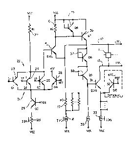
In the embodiment of Figure 1, the upper word line is
driven by a transistor 14 which has its emitter
connected to the word line and its collector connected to
a voltage VCC by a resistor 16. 'IKeep-alive" current is
supplied to the driver by a resistor 17 and a current
source 18, which also provide an additional pull-down
current during a falling transition on the word line.
Source 18 provides similar currents to driver
transistors in other stages of the circuit through
resistors similar to resistor 17. A clamping transistor
19 is connected to the collector of transistor 14 to
prevent saturation of the driver transistor.
The driver transistor is controlled by a 3-input EEL NOR
vale 21 which functions as an address decoder in an
input stage 22. The gate comprises transistors 23-25
which form one half of an EEL pair, with an additional
transistor 26 forming the other half of the pair. Input
signals Isle are applied to the bases of transistors
23-25, and a reference signal REV is applied to the base
of transistor 26. The collectors of transistors 23-25
are connected to a voltage VCC by a resistor 27, current
is supplied to the HOT, pair through a resistor 28 and a
transistor 29 connected to the emitters of the
transistors.
As long as all of the input signals Isle are "low",
transistors 23-25 are turned off, and the voltage at the
base of driver transistor I at a level near VCC, which
holds the driver "on" (i.e., a high output state) and
the word line connected to the driver in a selected
state. If any one or morn of the input signals is
.... ,.. " ......
"high", the base of transistor 14 is pulled down,
turning the driver "off" (i.e., to a low output state)
and deselecting the word line.
I I
--4--
In order to increase the rate at which the word line is
discharged and thereby reduce the transition time
between word lines, a transistor 31 and a current source
32 are connected to the lower word line 13 for supplying
a discharge current to the line. If desired, a second
transistor 33 can be connected to transistor 31 to form
an EEL pair and carry the discharge current.
A transistor 36 is connected to the collector of driver
transistor 14 for sensing a transition in the word line.
This transistor functions as an emitter follower, with
its base connected to the collector of the driver and an
additional pair of transistors 37, 38 connected in
series between the emitter of sensing transistor 36 and
the base of discharge transistor 31. These transistors
provide three stages of EEL level shift, and "keep-
alive" current for these transistors is provided by a
source 39.
When a word line transition begins, the voltage at the
base of driver transistor 14 falls quickly, which tends
to turn off the driver transistor, producing a transient
loss of current through resistor 16. The voltage at the
collector of transistor 14 increases by about 300 my,
and this pulse is transmitted by transistors 36-38 to
the base of transistor 31. Since transistor 31 shares a
large current source which is common to a number of
memory cells, it turns on strongly in response to the
300 my rise in its base-emitter voltage, thereby
applying a pull-down, or discharge, current to the lower
word line. When the emitter of transistor 14 is pulled
low enough in response to the falling word line,
transistor 14 begins to conduct again, terminating the
300 my pulse and shutting off the transient discharge
current.
-5- I
While this embodiment does provide some improvement in
access speed by reducing the time required to discharge
the word line, it has certain shortcomings. Resistor 16
in the collector of the word line driver tends to cause a
slight forward bias on the driver transistor, which
slows the response time of the device. The voltage at
the collector of the driver changes rather slowly due to
the relatively large transistor geometry which is
necessary for the levels of current the transistor must
handle. To minimize the current when the driver is in
the "low" or deselected state, resistor 16 must have a
relatively large value, which results in an undesirably
large ARC time constant at the collector of the driver.
An additional delay is produced by the propagation of
the signal through the three levels of shift provided by
transistors 36-38 before transistor 31 starts
conducting. The circuit also requires separate current
sources to assure a proper level at the collector of the
driver transistor when this transistor is "off" (i.e.,
on in its low output state) and to supply the "keep-alive"
current to the 3-stage level shifter formed by
transistors 37-39. These additional sources result in
an undesirably high power dissipation in the circuit.
The embodiment of Figure 2 is similar to the embodiment
of Figure 1 in a number of respects, and like reference
numerals designate corresponding elements in the two
embodiments. The embodiment of Figure 2 differs
significantly, however, with respect to the way a
word line transition is detected and the way signals are
applied to the discharge transistor.
In the embodiment of Figure 2, the collector of
transistor 26 on the right side of the CLUE pair in the
input stage is connected to the base of discharge
transistor 31 through a single emitter follower 41. A
resistor 42 is connected between the upper word line 12
--6--
and the base of transistor 41, and a clamping transistor
43 is connected to the collector of transistor 26 to
prevent saturation of this transistor.
As in the embodiment of Figure 1, as long as all of the
input signals Isle are "low", transistors 23-25 all
remain in an off state, and the base of drive
transistor 14 is high, holding this transistor on and
selecting the word line driven by it.
If any of the input signals becomes high, current is
lo steered to resistor 27, producing voltage drop across
this resistor which turns the driver transistor 14 "off"
(i.e., to a low output state) and deselects the word line
connected to it. With the driver in its low output
state, the voltage at the base of transistor 41 it
approximately equal to the voltage on the upper
word line. This transistor receives a small keep-alive
current from source 18 through resistor 17, and the
voltage at the emitter of the transistor sets the
voltage at the base of discharge transistor 31 such that
the base-collector junction of the discharge transistor
has a forward bias of about zero volts.
When a decoded address signal selects the word line
connected to driver 14, transistor 26 steers the current
from the EEL pair to resistor 42, which maintains the
discharge circuit in its off state by ensuring that the
voltage at the base of transistor 41 is low. The base
of transistor 41 remains low and thus prevents the high
discharge current from reaching word line 13 and loading
down a rising (selecting) transition.
An important feature of the embodiment of Figure 2 is
once driver transistor 14 shuts off or switches to a low
output state in a reselection step, the voltage at base
of transistor 41 rises very quickly toward the level of
--7--
word line 12. The rising voltage turns on transistor 41,
which then pulls up the base of discharge transistor 31.
Resistor 17 functions as a bleeder resistor which
provides current loading and allows the voltage at the
emitter of transistor 41 to move freely without
disturbing the voltage on the lower side of the
resistor. The rising pulse at the base of transistor 31
causes all of the discharge current to flow through the
lower word line and begin to pull the word line down. The
lo large discharge current continues until the voltage at
the collector of transistor 26 falls to the clamped
level set by transistor 43, at which point the discharge
current terminates.
In the embodiment of Figure 2, the transition is
detected in the input stage instead of the driver stage
as it is in the embodiment of Figure l. Thus, the
transition is detected a full stage earlier than it is
in the previous embodiment. This means that the full
discharge current it applied to the word line sooner,
which results in a shorter overall delay in the falling
(deselecting transition. In the rising (selecting)
transition, the discharge current is prevented from
reaching the word line, which permits a relatively fast
changing of thy word line. Moreover, in the steady state
selected and deselected conditions, only a small portion
of the discharge current reaches the lower word line to
satisfy set steady state voltage levels
the embodiment of Figure 2 thus has a number of
important features and advantages. The reselection
process is started sooner than in the previous
embodiment, and the discharge current reaches the
word line about one stage of delay sooner. The self-
terminating operation of the circuit provides a pulse
width which is determined by the speed of the node being
discharged. No oscillation occurs since the controlling
I
pulse is coupled directly to the word line. Transistor
41 provides additional gain which reduces the Miller
effect associated with the discharge transistor and also
provides level shifting to prevent saturation of the
discharge transistor. The collector of the word line
driver transistor 14 is connected directly to the
voltage VCC, which results in a further improvement in
speed. This circuit has fewer transistors than the
circuit of Figure 1, and power dissipation is reduced by
about 50 per cent due to the elimination of extra
current sources.
The embodiment of Figure 3 is similar to the embodiment
of Figure 2 in many respects, and like reference
numerals designate corresponding elements in the two
embodiments. In addition to improving the reselection
process by speeding up the discharging of the word line,
the embodiment of Figure 3 provides a further increase
in word line transition by speeding up the charging of
the word line during the selection process.
In the embodiment of Figure 3, a pull-up transistor 46
is connected to driver transistor 14 to turn that
transistor on more rapidly when the line connected to it
is addressed. Transistor 46 is connected as an emitter
follower, with its base connected to voltage VCC by a
resistor 47, and its emitter connected to the base of
the driver transistor.
In the input stage, transistors 23-25 are connected to
perform an logic OR function, with the collectors of
these transistors being connected directly to voltage
VCC, and the emitters being connected to voltage VIE by
a resistor 49 and a transistor 51.
The input stage also includes an EEL pair having
transistors 52, 53 on one side thereof and transistors
9 I I
54, 56 on the other. Current is supplied to the EEL
pair by a transistor 58 and a resistor 59 connected to
voltage VEER The level of current supplied to the EEL
pair is set by a control signal VCS applied to the base
S of transistor 58. This same signal is applied to the
base of transistor 49 and controls the level of current
through transistors 23-25. The output of the OR circuit
is applied to the bases of transistor 52, 53, and a
reference signal ROUGH is applied to the bases of
transistors 54, 560
The collector of transistor 52 is connected to the base
of driver transistor 14, and the collector of transistor
53 is connected to the base of pull-up transistor 46.
The collectors of transistors 54, 56 are connected to
the base of transistor 41 which controls the operation
of discharge transistor 31 as in the embodiment of
Figure 2. Transistors 52, 53 thus control the operation
of the driver transistor and the charging of the
word line, and transistors 54, 56 control the discharging
of the word line.
A clamping transistor 61 is connected to the emitter of
pull-up transistor 46 to turn off the pull-up transistor
and terminate the pull-up action when the voltage on the
base of the driver transistor 14 reaches a sufficient
level. In the embodiment illustrated, the emitter of
the clamping transistor is connected to a voltage of
-1.3 volts, and the clamping action occurs when the base
of the driver reaches a level of about -0.5 volts.
When the input signals Lowe all become low, transistors
52, 53 turn off, and the bass of drive transistor 14
and pull-up transistor 46 both rise toward the level of
voltage VCC. The pull-up transistor is thus turned on,
providing a low impedance path between VC~ and the base
of the driver transistor, which raises the voltage at
--10--
the base of the driver at a faster rate than it would
with only a passive connection to the power source.
With the base voltage rising faster, the driver turns on
sooner and the selection process is completed more
quickly than in the previous embodiments. As the
voltage at the base of the driver continues to rise, it
reaches a point where the base-collector junction of
clamping transistor 61 will be forward biased, at which
time the pull-up transistor turns off, terminating the
charging effect at the base of the driver Thus, the
pull-up transistor provides an initial transient pulse
of current at the outset of the selection process to
drive the rising transition at a faster rate than if it
were pulled up only by a passive resistor. Once the
pull-up transistor is turned off, the driver is held on
by the voltage applied to it by resistor 27 until a new
address is decoded by the OR circuit.
As soon as one of the input signals Isle goes high,
transistors 52, 53 are turned on, pulling down the bases
of driver transistor 14 and pull-up transistor 46,
switching the driver to its low output state to initiate
the reselection process. At the same time, transistors
54, 56 are turned of, allowing the voltage at the base
of transistor 41 to rise quickly toward the level of the
upper word line. initiating the pulse for discharging the
word line as in the embodiment of Figure 2.
The embodiment of Figure 3 has the advantages of the
embodiment of Figure 2 from the standpoint of providing
a relatively fast discharge ox a deselected word line.
In addition, it starts the selection process more
quickly, and the faster rising transition allows the
newly selected word line to reach its high state more
quickly, thereby improving access time even further.
-11- I I
It is apparent from the foregoing that a new and
improved memory selection circuit has been provided.
While only certain presently preferred embodiments have
been described in detail, as will be apparent to those
familiar with the art, certain changes and modifications
can be made without departing from the scope of the
invention as defined by the following claims.