Note: Descriptions are shown in the official language in which they were submitted.
204~546
TITLE OF THE INVENTION
THYRISTOR CONVERTER PROTECTION METHOD
AND APPARATUS
BACKGROUND OF THE INVENTION
Field of the Invention:
The present invention relates generally to a protection
method and apparatus for thyristors in a power converter and
more particularly to a protection method for thyristors using
forced triggering signals.
Discussion of the Background:
Thyristors are commonly used in power converters and
similar applications. The thyristors may be arranged in a
series connection or a series-parallel connection. While
these devices have become common, a certain type of failure
may occur when an unusual transient pulse occurs during a
certain period of operation of the device.
Figure 1 shows a prior art thyristor converter that is
used for direct current power transmission. Incoming power is
converted from alternating current to direct current or vice
versa utilizing transformer 12 and thyristor converter 10.
Reactor 13 helps to smooth the resultant current. An arm of
the thyristor converter 10 is shown in Figure 2 as including a
number of thyristor converters 16l..16~..16N arranged in series.
The thyristors shown are light thyristors that are also
-2- 2042546
connected to individual voltage dividing circuits 18l. .181..18N
which serve to make the thyristor voltages uniform. Light
guides 141..14l..14N are light guides which transmit the trigger
light signals from a pulse generator (not shown) to the
respective thyristors. Arrestor 15 serves to suppress
thyristor overvoltage. The number of thyristors, N, which are
arranged in series is determined by the voltage rating of the
converter.
Figure 3 shows graphs of thyristor voltage and current
over a period of time, when operating as an inverter. Circuit
voltage ~, determined by the main circuit, is imposed on the
thyristor. At time tl this voltage falls to zero and the
thyristor becomes conductive as seen by the graph of the
thyristor current. At time t2 the thyristor is turned off and
circuit voltage ~ is made negative. Since carriers remain
inside the thyristor immediately after conduction, it is not
possible to immediately achieve a forwardly-directed withstand
voltage (forward recovery), but it is necessary first to
impose a set reverse voltage period until the carriers are
removed. This reverse voltage period is known as the margin
angle, ~. If this reverse voltage period is too small,
commutation failure may occur in the converter as a whole or
there may be an occurrence of partial commutation failure
known as partial self-triggering. This occurs when series
connected thyristors include some elements in which triggering
occurs and some elements where it does not occur. When this
Z0~2546
-3-
happens, the entire circuit voltage is then imposed on the
elements where triggering does not take place. This results
in the element breaking down due to overvoltage or element
breakdown due to a self-triggering domino effect which
accompanies a rise in voltage above a certain level. In order
to compensate for this, other prior art devices have made use
of forced triggering protection where triggering signals are
forcibly supplied if the margin angle becomes too small due to
a decrease in system voltage, voltage distortion or improper
control. This protection helps prevent excessive stress on
elements and prevents element breakdown. Thus, forced
triggering is known to prevent self-triggering of thyristors
during times of overvoltage or when the voltage is above a
dangerous level. However, this approach has only been used
during the margin angle (reverse voltage) period.
Specifically, it has not proved satisfactory when overvoltage
enters the converter immediately after conduction.
At time t2 shown in Figure 3, ~ assumes a reverse voltage
to start the margin angle. This period ends at time t3, when
becomes zero.
The thyristor recovery voltage E~ gradually increases when
the residual carriers disappear during the margin angle. This
voltage starts to increase from zero at a time t20. This
voltage increases and eventually crosses the voltage level V~
which corresponds to the protection level provided by the
arrestor 15. It then continues until it reaches the forward
204Z5~6
withstand voltage VD~ at time t6. For a high withstand
voltage, large current thyristor, the time necessary to
achieve forward recovery varies considerably within the range
of 1.2 to 1.5 Tq, where Tq is the on-off time. This forward
recovery time is seen in the figure as the time between t2 and
t6 .
As can be seen from Figure 3, in normal operation E~ is
greater than ~ during the forward recovery time. Thus, the
thyristor forward recovery voltage is always higher than the
circuit voltage. However, during this time if a forwardly
directed overvoltage occurs such as indicated by the dashed
line at t~, the circuit voltage may become greater than the
forward recovery voltage for a short time. The thyristor may
be unable to withstand this lower voltage and accordingly, the
problem of self-triggering occurs. The thyristor will then
breakdown if the voltage is above a certain value (designated
as the limit self-triggering voltage V~). V~ may be
approximately one-third to one-half of VD~. Since the
occurrence of an overvoltage is random and may occur at any
time, it is necessary to protect the thyristor elements during
the time period of t2 to t5. After t5 there is no problem since
there is satisfactory recovery to the forward withstand
voltage. During the time period t2 to t3 (the margin angle),
it is possible to utilize conventional force triggering
protection as described above. However, during the time
period t3 to t5, prior art devices cannot provide protection.
2042546
-5-
Accordingly, during this vulnerable period the thyristors may
breakdown due to overvoltage.
SUMMARY OF THE INVENTION
Accordingly, one object of this invention is to provide a
novel method and apparatus for applying a forced triggering
signal to all thyristors when an overvoltage is applied.
It is another object of the present invention to provide
a novel method and apparatus for forecasting the imposition of
a forwardly-directed overvoltage immediately after the
termination of the thyristor current.
It is another object of the present invention to detect a
high voltage at each thyristor and to impose a forced trigger
signal to all thyristors when an overvoltage occurs.
It is a still further object of this invention to provide
a novel method and apparatus for protecting thyristors by
detecting voltages at each thyristor and imposing a forced
supply of triggering signals if the overvoltage occurs during
the desired protection period.
It is a still further object of the present invention to
provide a novel method and apparatus for protecting thyristors
by applying a forced trigger pulse to the thyristors if either
a voltage higher than a set level or a voltage rise rate which
exceeds a set value is detected in the forward voltage
recovery protection period.
204Z546
--6--
BRIEF DESCRIPTION OF THE DRAWINGS
A more complete appreciation of the invention and many of
the attendant advantages thereof will be readily obtained as
the same becomes better understood by reference to the
following detailed description when considered in connection
with the accompanying drawings, wherein:
Figure 1 is a block diagram of a prior art thyristor
converter;
Figure 2 is a block diagram of a thyristor valve in
Figure 1;
Figure 3 is a graph describing the voltage and current of
the device shown in Figure 2;
Figure 4 is a block diagram of the first embodiment of
the present invention;
Figures 5a and Sb are time charts of various signals
which occur in the apparatus of Figure 4 during normal
conditions and overvoltage conditions, respectively;
Figure 6 iS a block diagram of a second embodiment of the
present invention;
Figure 7 is a block diagram of the forward recovery
protection circuit shown in Figure 6;
Figure 8 is a block diagram of the period setting circuit
shown in Figure 7;
Figure 9 is a time chart of signals which occurs in
Figures 7 and 8;
2042S~6
-7-
Figure 10 is a block diagram of a second embodiment of
the period setting circuit shown in Figure 7;
Figure 11 is a time chart of signals shown in Figure 10;
Figure 12 is a block diagram of a third embodiment of the
present invention; and
Figure 13 is a block diagram of a fourth embodiment of
the present invention.
DESCRIPTION OF THE PREFERRED EMBODIMENTS
Various other objects, features and attendant
advantages of the present invention will be more fully
appreciated as the same becomes better understood from the
following detailed description when considered in connection
with the accompanying drawings in which like reference
characters designate like or corresponding parts throughout
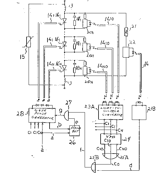
the several views and wherein Figure 4 shows the first
embodiment of the present invention. Thyristors 16l..16l..16N
are arranged in series between reactors 13 and in parallel to
arrestor lS. Light guides 141..14l..14N transmit light signals
to trigger the thyristors. Voltage dividing circuits 18l..
181. .18N and forward voltage detection circuits 201..20l..20N are
provided for each thyristor. The forward voltage detection
circuits determine the forward voltage for each thyristor and
transmit a light signal indicative of this voltage through
light guides 14~o..14~o..14NO. These light signals are then
converted back to voltage signals Cl..CI..CN in circuit 23a.
- ~- 204254fi
_ -8-
Thus, each of these signals indicates the forward voltage for
each corresponding thyristor.
At the same time, an overvoltage for the thyristor valve
as a whole (total voltage of the elements) is detected by
overvoltage detection resistor 21 and overvoltage detection
circuit 22. This voltage is also converted to a light signal
and transmitted to a converter circuit 23b to reform an
electrical signal, d. The overvoltage detection level in
circuit 22 is set at slightly lower than N times the self-
triggering voltage limit, V~ (shown in Figure 3). Thus,
overvoltage signal d indicates that the circuit as a whole has
reached a dangerous overvoltage condition.
A forward voltage signal processing circuit 24 detects
the forward voltage signal for each thyristor and determines
whether each signal has reached zero. When the zero level is
reached, output signals C~0..CI0.. CNO are produced. The signals
are combined in an OR gate 25A to produce output CO.
Similarly, this signal and signal d are combined in OR gate
25B to produce output signal f. Thus, this signal provides an
indication that at least one of the thyristors or the circuit
as a whole has an unusual forward voltage signal.
A protection period setting circuit 26 determines the
protection period for the device. That is, it determines the
period t3 - tS during which time the thyristors are vulnerable
to an overvoltage failure. Output signal e is indicative of
this time period. The period setting circuit receives input
. . .
2042S46
signal a which starts at time tl and ends at time t2. This
signal is indicative of the conduction period and is usually
120. This signal is received from a converter control unit
(not shown). Signal b, which is indicative of the reverse
voltage period (margin angle) t2 - t3 is also received by the
period setting circuit. This signal allows the period setting
circuit to determine the beginning of the protection period
signal e. This signal is received by AND gate 27 which also
receives signal f. When both signals are present, a signal g
is given to gate pulse generator 28 which then outputs light
signals through the light guides 141..14I..14N to forcibly
trigger the thyristors. This then protects the thyristors
during the invulnerable time t3 tS but only if an overvoltage
situation is sensed either in an individual thyristor or in
the circuit as a whole.
Gate pulse generator 28 also produces other signals. The
generator receives forward voltage signals C~..CI.. CN from the
circuit 23A. Signal b is produced by the end of signal a and
the beginning of the C signals.
The end point of signal e is determined in the period
setting circuit 26 by setting the maximum value expected for
the length of this pulse.
Figure 5a shows the normal operation of the device of
Figure 4 without an overvoltage while Figure 5b shows the
operation of the same device when an overvoltage occurs. The
top line in each figure is similar to the timing chart in
2042546
--10--
Figure 3 except that two different lines are provided for E~.
This is to indicate a range of possible voltages which occur
normally in slightly differing thyristors. In Figure 5b, the
overvoltage signal is indicated by a dotted line. In both
figures, signals a and b indicate the respective time periods
tl - t2 and t2 - t3. Under normal conditions, the various C
signals detect a zero voltage at time t3 and stay at the "1"
voltage level since no overvoltage is determined. On the
other hand, in the overvoltage situation, the C signals start
at the "1" level at time t3 and change to the "O" level at
times t3B - t3D. There are slight differences in the sensed
times since there are slight differences in the
characteristics of the various thyristors. However, at their
individual times self-triggering occurs. The first self-
triggering signal Cl causes signal C0 to occur. This then also
causes the generation of signal g from AND gate 27 since it
occurs during the time period t3 - t5, as determined by signal
e. Signal g then causes forced triggering signals to be
supplied to all the thyristors.
In the example shown, signal d is not produced since
self-triggering takes place before the overvoltage reaches the
overvoltage detection level VO~ for the thyristor valve as a
whole. However, if an overvoltage occurs where the voltage is
comparatively low and the change in voltage over time is small
and occurs during the time period t4 - tS~ it may be difficult
for self-triggering to take place. As a result, the
2042546
--11--
overvoltage is detected when it becomes greater than the
detection level and an overvoltage signal d and forced
triggering signal g are produced to cause forced triggering
signals to be supplied to the thyristors.
Although the protection period has been set at t3 - t5, it
is also possible to instead use the protection period as t2 ~
t5 and omit the conventional protection for forced triggering
when the margin angle is small. This can be done by setting
the period setting circuit 26 to produce signal e at the
beginning of received signal b rather than the end thereof.
One form of converter control protection action is to
cause gate shifts. If there are concerns that this could
cause unwanted action by self-triggering detection signals C0
and overvoltage detection signals d, it is possible to
temporarily lock these two signals by the gate shift signals.
The above embodiment utilizes a single signal processing
arrangement which receives signals from detectors associated
with each of the thyristors. It is also possible to instead
utilize a detection device which detects only voltage from one
representative thyristor.
The second embodiment of the invention is shown in Figure
6. Voltage detector 20 detects the voltage or rate of change
of the voltage of thyristor 16. A voltage divider circuit 18
is connected to the thyristor in a manner similar to Figure 4.
Likewise, the reactor 13 is connected to one terminal of the
thyristor. The voltage detector 20 is a circuit made of
20425~
-12-
resistors or a combination of a resistor and a capacitor. The
detected voltage is received by forward voltage recovery
protection circuit 32 which serves to determine the protection
period and to detect overvoltages. A forced trigger signal
may then be applied to the thyristor. A light triggering
signal is carried by light guide 14 and converted to a voltage
signal a. This signal is amplified to produce signal b which
is applied to the thyristor and which determines the turn on
period of the thyristor. Signal a is also applied to the
overvoltage recovery protection circuit to determine the
proper time protection.
Figure 7 shows a more detailed block diagram of the
forward voltage recovery protection circuit 32. A protection
period setting circuit 34 receives input signal a and voltage
detection circuit c from the voltage detector 20 to determine
the protection period which lasts for a set time from zero
voltage t3. An overvoltage detection circuit 36 receives
output c from the voltage detector 20 and produces an
overvoltage signal e if it exceeds a set level (VOL shown in
Figure 9). If AND gate 38 receives signal e at the same time
as signal d representing the desired protection period, a gate
trigger signal command is produced and amplified in amplifier
40 to produce forced trigger signal f which is applied to the
thyristor gate as shown in Figure 6.
Figure 8 shows one embodiment of the protection period
setting circuit 34. Input signal a is applied to an inverter
2042546
-13-
100 whose output g is received by AND gate 103. Input signal
c is received by diode 101 which is connected to voltage
detector 102. The output of the voltage detector, signal h,
is also applied to AND gate 103. The output of AND gate 103,
signal i, is applied to one shot multivibrator 104 which
produces output signals d.
Figure 9 shows a time chart of the various signals found
in Figures 6, 7 and 8. The top line is similar to the time
charts in Figures 3 and 5. As can be seen in the figure,
signal g is merely the inverse of signal a. Signal h is
produced by the voltage detector 102 when signal c reaches the
zero point at t3. The conjunction of these two signals in AND
gate 103 causes one shot 104 to produce a signal d of width
~t.
Figure 10 shows another embodiment of the circuit shown
in Figure 8. However, in this circuit input c is also applied
to diode 105 and a second voltage detector 106. A voltage
detector determines when the voltage of c is negative, that
is, t2 - t3. This produces signal j which is combined with
signal d from one shot 104 in OR gate 107 to produce a new
output signal d'.
Figure 11 shows signals j and d' from Figure 12. As can
be seen, signal j merely adds the margin angle to the existing
~t in the OR gate to produce the output d' which includes the
time t2 - t5. As mentioned above in regard to Figures 4 and 5,
2042546
-14-
the protection signal may be extended to include the margin
angle desired.
Figure 12 shows another embodiment of the present
invention. In this embodiment, the thyristors utilized are
electrical and light trigger thyristors which have both
electrical and light trigger inputs. The same forward
recovery protection found in Figure 6 may be possible by
replacing the single branch type light guide 14 of Figure 6
with a partially branched light guide 14l (2-branch type).
Figure 13 shows another embodiment of the present
invention used with light trigger thyristors. The light guide
14 of Figure 6 is replaced by a 2 x 2 branched light guide 142
in order to have the same forward recovery protection as in
Figure 6. A gate trigger command signal, a, is partially
branched at point A and leads to photoreceptor element 42 of
the FR protection circuit 32. The output of the protection
circuit 32 is sent through light-emitting element 44 and
reenters the light guide at point B so that signals bl (which
is the same as A) and b2 both enter the thyristor.
The embodiments described above make it possible to
ensure a forced triggering protection against overvoltage
during the period immediately after the thyristor turn off in
a system where each thyristor is provided with a voltage
detector and a FR protection circuit. Since protection is
effected for each individual thyristor in the series,
protection is provided at high speed and it is possible to
2~)425~6
-15-
protect the device even against very fast lightning surge
overvoltage.
Having now fully described the invention, it will be
apparent to one of ordinary skill in the art that many changes
and modifications can be made thereto without departing from
the spirit or scope of the invention as set forth herein.