Note: Descriptions are shown in the official language in which they were submitted.
OF867
204267~
ADAPTIVE EQUALIZER WITE~ MIDBURST CORRECTION CAPABILITY
BACKGROUND OF THE INVENTION
This invention relates to an adaptive equalizer for
reducing intersymbol interference in digital communication
apparatus that receives differentially encoded data.
Differentially encoded binary phase-shift keying (BPSK)
and quadrature phase-shift keying (QPSK) are widely used in
cellular radio systems for communication between a base
station and mobile stations such as automobile-mounted
telephones. The mobile receiver generally includes an
equalizer: a digital filter that compensates for
transmitter filtering and channel conditions.
Cellular communication is performed on a time-division
multiple-access basis and takes place in a series of short
bursts. A burst commences with the transmission of fixed
training data to enable the equalizer to adapt its filter
coefficients, then continues with user data, during the
reception of which the equalizer further adapts its filter
coefficients to track channel variations.
The equalizer can adapt to gradual channel variations,
but cannot follow abrupt changes. When such abrupt changes
occur, the equalizer may lose track of the channel
condition. If the equalizer wanders too far from the
correct channel condition, received data values will be in
OF867
204267~
error.
One way to reduce such errors is to perform a midburst
correction using known data, such as a color code occurring
at a fixed intermediate location in the user data. ~ue to
the phase ambiguity of differential encoding, however, the
receiver cannot tell which of the possible encodings of the
known data to employ as desired data for the midburst
correction. For this reason, existing adaptive equalizers
have been unable to take advantage of known data occurring
midway through a burst.
SUMMARY OF TIIE INVENTION
It is accordingly an object of the present invention to
make use of known data occurring at an intermediate point in
a differentially encoded data burst to correct the filter
coefficients of an adaptive equalizer.
An adaptive equalizer has adaptive filter means for
filtering sample values according to certain coefficients,
thus producing a filtered value, then updating the
coefficients according to an error value. A detector means
detects the filtered value to produce a symbol value, which
is the ou1put of the adaptive equalizer.
The error value is generated by an error feedback means
as the difference between the filtered value and a desired
value. During reception of user data, the symbol value is
- ~04267~
the desired value.
Prlor to reception of known data embedded in the
user data, a storage means saves the internal state of the
adaptive filter means. When the known data are recelved they
are placed in the storage means, then repeatedly supplled to
the adaptive filtered means and filtered, starting from the
internal state saved in the storage means. Durlng thls time,
a known-data generating rneans produces different differential
encodings of the known data as desired data.
An accumulator rneans adds the error values to
produce a cumulative error value for each differentlal
encoding. A comparator means compares the cumulatlve errors
and dlrects the known-data generatlng means to generate the
differential encoding that produced the least cumulative error
once again, so that the fllter coefficients can be adapted to
the optimum values. Reception of user data then continues.
In accordance with the present invention there ls
provided an adaptive equalizer for reducing lntersymbol
interference ln a received burst of differentially encoded
data havlng known data at an interrnediate location in the
burst, cornprising: input means for receivlng sample values;
adaptive filter means, connected to said input means, for
filtering said sample values accordlng to certaln coefflclents
to produce a flltered value, and updating said coefflclents
according to an error value; detector means, connected to sai-l
adaptive filter rneans, for detecting said filtered value and
producing a symbol value; output means, connected to said
detector rneans, for output of said symbol value; known-data
27948-6
2û4267~
generatinq rneans, for producing different differential
encodings of sald known data; error feedback means, connected
to said adaptive filter means, said detector means, and said
known-data generating means, for calculatlng said error value
as a difference between said filtered value and a desired
value, said desired value being generated by said known-data
generating rneans during reception of said known data;
accumulator means, connected to said error feedback means, for
surnming sald error values to produce, for each of said
differential encodlngs, a cumulative error value for that
differential encoding, comparator means, connected to said
accumulator means and said known-data generating means, for
finding a cumulative error with minimurn absolute value and
causlng said known-data generatlng means to generate the
corresponding differential encoding of said known data again;
and storage means, connected to said input means and sald
adaptive filter, for saving an internal state of sald adaptive
fllter means recelvlng and storing sample values corresponding
to said known data, then repeatedly restoring said adaptive
fllter means to the saved lnternal state and repeatedly
supplying the stored sample values to said adaptive fllter
means.
In accordance with the present inventlon there is
also provided an adaptive equalizer for reducing lntersymbol
interference in a received burst of differentially encoded
data having known data at an intermediate location in the
burst, comprising: an input circuit coupled to receive sarnple
values; an adaptive filter clrcult coupled to said input
r 3a
27 948 - 6
' 204267~
circuit and configured to filter the sample values according
to coefficients to produce a filtered value, the adaptive
filter circuit being effective to update the coefficients in
accordance with an error value; a detector coupled to said
adaptive filter circuit to provide a symbol value; a known
data generator circuit configured to produce different
differential encodings of the known data; an error feedback
calculating circuit coupled to said adaptive filter circuit,
said detector, and said known data generator circuit, the
error feedback calculating circuit being configured to
calculate said error value as a difference between the
filtered value and a desired value, the desired value being
generated by the known data generator circuit; an accumulator
circuit coupled to said error feedback calculating circuit
thereby to provide a cumulative error value for each of said
different differential encodings; a comparator circuit coupled
to said accumulator circuit and the known data generator
circuit, the comparator circuit being configured to find the
said cumulative error with the smallest absolute value, the
known data generator circuit being responsive to the compara-
tor circuit to generate the corresponding differential
encoding of the known data again; a storage circuit coupled to
said input circuit and said adaptive filter circuit, said
storage circuit being configured to store sample values
corresponding to said known data and to restore the adaptive
filter circuit to an internal state saved in said storage
circuit, and to supply stored sample values to the adaptive
filter circuit; and an output path coupled to said detector.
3b
27948-6
- 204267~
In accordance with the present invention there is
further provlded a method for adaptively equalizing and
reducing intersymbol interference in a received burst of
differentially encoded data having known data at an
intermediate location in the burst, comprising the steps of:
receiving sample values; filtering said sample values
according to certain coefficients to produce a filtered value,
and updating said coefficients according to an error value;
detecting said filtered value and producing a symbol value;
outputting said symbol value; producing different differential
encodings of said known data; calculating said error value as
a difference between said filtered value and a desired value,
said desired value being generated during reception of said
known data; summing said error values to produce for each of
said differential encodings a respective cumulative error
value; finding the cumulative error with lowest absolute value
and generating the corresponding differential encoding of said
known data again; saving an lnternal state for said filtering;
receiving and storing sample values corresponding to said
known data; then repeatedly restoring the saved lnternal state
and repeatedly supplying said stored sample values for said
filtering.
~RIEF DESCRIPTION OF THE DRAWINGS
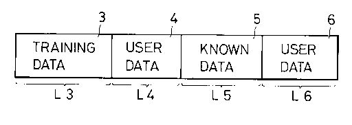
Fig. 1 illustrates a data burst having known data at
an intermediate location.
Fig. 2 is a general block diagram of the invented
adaptive equalizer.
3c
.~ 27g48-6
204267~
Flq. 3 is a more detailed block diagrarn of the input
means, adaptive fllter, and storage means ln Fig. 2.
3d
27948-6
OF867
204267~
Fig. 4 is a more detailed block diagram of other
components shown in Fig. 2 in a first embodiment of the
invention.
Fig. 5 is a more detailed block diagram of other
components shown in Fig. 2 a second embodiment of the
invention.
DETAILED l)ESCRIPTION OF THE INVENTION
Fig. 1 illustrates the structure of a data burst of the
type used, for example, in time-division multiple-access
cellular communications systems. The burst begins with a
training field 3 consisting of a certain number (L3) of
predeterm;ned symbols. The number of symbols in a field
will be referred to hereinafter as the length of the field.
A symbol represents one or more logic values, depending
on the type of modulation employed. In BPSK modulation, for
example, a symbol represents the logic value O or 1. In
QPSK modu]ation a symbol represents OO, O1, 10, or 11.
The training field 3 is followed by a first user data
field 4 of length L4, then a known data field 5 of length
L5, then a second user data field 6 of length L6. The two
user data fields 4 and 6 contain, for example, a brief
interval of digitally encoded speech in a telephone call.
The known data field 5 contains, for example, a color code
used to discriminate bursts from different cells employing
OF867
20426~
the same frequency. The color code is received from the
base station at the beginning of a call and remains fixed
throughout the call.
Next a general description of the invented adaptive
equalizer will be given with reference to Fig. 2. It should
be understood that Fig. 2 and the other attached drawings do
not restrict the scope of the invention, which should be
determined solely from the appended claims.
The adaptive equalizer in Fig. 2 comprises an input
means 100 for input of sample values y(n) that have been
obtained, for example, by demodulating a signal received at
an antenna and passing the demodulated signal through an
analog-to-digital converter. The sample values are
according]y digital values comprising, for example, sixteen
bits each, all data paths shown in Fig. 2 being sixteen bits
wide in this case. The sample rate is the same as the data
rate, one sample covering the time span of one symbol, but
due to intersymbol interference, the information in a symbol
is spread over a plurality of consecutive samples.
The sample values are supplied from the input means 100
to an adal~tive filter means 110 that performs a filtering
operation using coefficients Ci to obtain a filtered value
z(L). The operation that produces z(L) involves a plurality
of values such as sample values y(L+N) to y(L-M), where
N > O and M > O. The effect of filtering is to reduce
. OF867
20426~
intersymbol interference, so that substantially all of the
information in a single symbol is contained in a single
filtered value z(L). After calculating z(L), the adaptive
filter means 110 updates the coefficients Ci in preparation
for the next filtering operation.
The filtered value z(L) is passed to a detector means
120 that E)erforms a thresholding operation to produce a
symbol va]ue x(L). While the filtered value z(L) has a
substantially continuous range of values, the symbol value
x(L) can take on only certain specific values in this range,
such as the values +1 and -1 when BPSK modulation is used.
In genera], the detector means 120 generates the symbol
value closest to the filtered value z(L). The symbol value
x(L) is sent to an output means 130 such as a data bus, to
undergo further digital processing by external devices not
shown in the drawings.
The filtered value z(L) is also furnished to an error
feedback means 140 which subtracts a desired value to
produce an error value e(L). The symbol value x(L) can be
supplied to the error feedback means 140 as the desired
value, or other desired values can be used as described
below. The error value e(L) is returned to the adaptive
filter means 110 for use in updating the coefficients Ci.
The adaptive equalizer further comprises a training-
data generating means 150 such as a memory device in which a
OF867
20~267~
sequence of training symbols is stored for provision to the
feedback means 140 as desired values.
The adaptive equalizer also has a known-data generating
means 160 which generates all possible differential
encodings of the known data field 5 in Fig. 1, for provision
to the feedback means 140 as desired values. The known-data
generating means 160 may comprise a register or memory
device in which the known data are stored and a computing
device for differentially encoding the known data and
producing different encodings as required. Alternatively,
the known-data generating means 160 may simply comprise
memory means in which the different differential encodings
are placed by an external computing device.
The error values e(L) generated by the error feedback
means 140 can also be supplied to an accumulator means 170,
which sums them to produce a cumulative error value.
Cumulative error values calculated in this way are supplied
to a comparator means 180 which compares them, determines
which is smallest in absolute value, and directs the known-
data generating means 160 to generate the corresponding
differential encoding once again.
The adaptive equalizer also comprises a storage means
190 which is connected to the input means 100 and the
adaptive filter means 110 and has four functions: saving
the internal state of the adaptive filter means 110;
204267~
OF867
restoring the adaptive filter means 110 to the saved
internal state; storing input sample values y(n); and
repeatedly supplying the stored sample values to the
adaptive filter means 110.
Next the operation of the adaptive equalizer will be
described, again with reference to Figs. 1 and 2.
During reception of the training field 3 in Fig. 1, the
sample values y(n) received at the input means 100 are
supplied to the adaptive filter means 110 and filtered, and
the resulting filtered values z(L) are sent to the error
feedback means 140. From these filtered values the error
feedback means 140 subtracts the symbol data supplied by
training-data generating means 150 to generate error values
e(L). These are returned to the adaptive filter means 110
and used to update the coefficients Ci. By the end of the
training field 3, the coefficients have become adapted to
current channel conditions and equalization is being
performed accurately.
During reception of the first user data field 4 in Fig.
1, the received sample values y(n) are filtered by the
adaptive filter means 110, and the filtered values z(L) are
detected by the detector means 120 to produce symbol values
x(L). These symbol values are furnished as output to the
output means 130, and as desired values to the error
feedback means 140. The adaptive filter means 110 updates
204267~
OF867
the coefficients Ci on the basis of the error values e(L),
where e(L) = z(L) - x(L). At the end of reception of the
first user data field 4, the storage means 190 stores the
current state of the adaptive filter means 110.
During reception of the known data field 5, the sample
values y(n) are not supplied from the input means 100 to the
adaptive filter means 110, but are instead stored in the
storage means 190. Then the following operation is carried
out once for each differential encoding of the known data:
the accumulator means 170 is cleared to zero; the sample
values y(n) stored in the storage means 190 are sent to the
adaptive filter means 110 and filtered; the resulting
filtered values z(L) are sent to the error feedback means
140, which subtracts the encoded symbol values supplied by
the known-data generating means 160 to generate error values
e(L); the error values e(L) are returned to the adaptive
filter means 110 and used to update the coefficients Ci; and
the error values e(L) are summed in the accumulator means
170. Each time this operation is completed, the cumulative
error value in the accumulator means 170 is transferred to
the comparator means 180 and stored, and the adaptive filter
means 110 is restored to the state saved in the storage
means 190.
When this operation has been completed for every
different~al encoding of the known data field 5, the
Z04267~
OF867
comparator means 180 determines which encoding produced the
smallest cumulative error. Then the known-data generating
means 160 supplies that encoding to the error feedback means
140 as desired values while the sample values y(n) stored in
the storage means 190 are once again sent to the adaptive
filter means 110 and filtered. As before, the error
feedback means 140 produces error values e(L), on the basis
of which the adaptive filter means 110 updates the
coefficients Ci. In addition, the filtered values z(L) are
detected and the resulting symbol values x(L) are sent as
output to output means 130. When the adaptive equalizer has
output the last symbol value x(L) in the known data field 5,
the adaptive filter means 110 remains in its current state,
retaining the last updated values of the coefficients Ci.
In this way, the adaptive equalizer finds the
differential encoding of the known data field 5 that best
fits the sample values actually received, and uses that
encoding as desired values to re-adJust the coefficients Ci.
According]y, even if the adaptive equalizer had lost track
of channe] conditions during reception of the first user
data field 4, it is able to recover during the known data
field 5 and resume correct equalization.
During reception of the second user data field 6, the
adaptive equalizer operates in the same way as during
reception of the first user data field 4.
20~267~
OF867
Symbol values are thus output for the first user data
field 4, the known data field 5, and the second user data
field 6. If the symbol values x(L) output for the known
data field 5 match the known data correctly, the burst is
assumed to be valid and the user data can be further
processed. If the symbol values x(L) output for the known
data field 5 do not match the known data, the burst is
assumed to be invalid, belonging to a call in a different
cell for example, and the user data can be ignored.
Next two more detailed embodiments of the invention
will be described, the first suitable for BPSK modulation
and the second suitable for QPSK modulation. The two
embodiments are substantially identical with respect to the
input means 100, the adaptive filter means 110, and the
storage means 190, which will be illustrated for both
embodiments in Fig. 3. The other components will be
illustrated separately for the two embodiments in Figs. 4
and 5.
Referring to Fig. 3, sample values y(n) are received at
an input bus 201 and fed via switches (described later) to a
first shift register 202 having M + N + 1 stages, where
M > 0 and N > 0 as before. Each stage is indicated by a
square box in the drawing and is capable of holding one
sample value y(n) comprising, for example, sixteen bits.
Between each pair of ad~acent stages in the first shift
204;~674
OF867
register 202 is a switch 203 having two inputs and one
output. The output of each switch 203 feeds the next stage
of the first shift register 202. The first input (1) of
each switch 203 is connected to the output side of the
preceding stage of the first shift register 202. The second
input (2) of each switch 203 is connected to a storage
register 204. The first stage of the first shift register
202 is also preceded by a switch 203, the first input (1) of
which is connected (via switches described later) to the
input bus 201.
The storage register 204 resembles the first shift
register 202 in having M + N + 1 stages, each capable of
holding one sample value y(n). The output side of each
stage of the storage register 204 is connected to the second
input (2) of the switch 203 preceding the corresponding
stage of the first shift register 202.
The input side of each stage of the storage register
204 is connected to the output side of a switch 205 having
~ust one input and one output. The input of the switch 205
is connected to the output side of the corresponding stage
of the first shift register 202.
The adaptive equalizer also comprises M + N + 1
multipliers 206, one for each stage of the first shift
register 202. Each multiplier 206 receives the sample value
y(n) stored in the corresponding stage of the first shlft
2042674
OF867
register 202, multiplies it by a coefficient, and supplies
the resulting product to an addlng means 207. The
coefficients are denoted C-N to CM in the drawing.
The coefficients C-N to CM are supplied to the
multipliers 206 from a coefficient updating means 208. The
coefficient updating means 208 is, for example, a digital
signal processor with various internal registers, not
explicitly shown in the drawing, for storing values used in
calculating the coefficients.
The adding means 207 adds the products received from
the multiI)liers 206 and supplies their sum as the filtered
value z(L) to a first node 209. The function of the first
node 209 is simply to connect the adding means 207 in Fig. 3
to components that will be shown in Fig. 4 or 5. A second
node 210 similarly connects the coefficient updating means
208 to components in Fig. 4 or 5.
Referring now to Fig. 4, which pertains to the first
embodiment, the filtered value z(L) is supplied from the
first node 209 to a sign detector 211 and a subtractor 212.
The sign detector 211 generates a symbol value x(L) of ~1 or
-1 according to whether the sign of the filtered value z(L)
is positive or negative.
The symbol value x(L) is fed to the first input (1) of
a switch 213 having four inputs and one output. The output
of the switch 213 is supplied as a desired value to the
2~4267~
OF867
subtractor 212, which subtracts the desired value from the
filtered value z(L) received from the first node 209 to
produce an error value e(L).
The second input (2) of the switch 213 is connected to
a training data memory 214 in which is stored a copy of the
training field 3 in Fig. 1. The third input (3) of the
switch 213 is connected to a first known-data memory 215, in
which is stored a differentially encoded copy of the known
data field 5 in Fig. 1. The fourth input (4) of the switch
213 is connected to a second known-data memory 216, in which
is stored the opposite differential encoding of the known
data field 5. That is, the values stored in the first and
second known-data memories 215 and 216 have opposite signs.
For example, if the known data field 5 is
[+l, -1, +1, +1, +1, -1, -1],
then the encoded value stored in the first known-data memory
215 could be
[+l, -1, -1, -1, -1, ~1, -1],
in which case the opposite encoded value stored in the
second known-data memory 216 is
14
204267~
OF867
[-1, +1, +1, +1, +1, -1, +1].
These values are placed in the first and second known-data
memories 215 and 216 at the beginning of a call, for
example, and remain unchanged for the duration of the call.
The error value e(L) produced by the subtractor 212 is
supplied to the second node 210 for return to the
coefficient updating means 208 in Fig. 3, and is also
supplied to an adder 217. The adder 217 adds the error
value e(L) to the contents of an error accumulator 218, and
places the resulting sum in the error accumulator 218.
The output of the error accumulator 218 is supplied to
a switch 219 having one input and two outputs. The first
output (1) of the switch 219 is connected to a first error
memory 220; the second output (2) is connected to a second
error memory 221. The values stored in the first and second
error memories 220 and 221 are both supplied as inputs to a
comparator 222, which compares them, determines which is
smaller in absolute value, and notifies a control means 223.
The control means 223 controls the switch 213.
The symbol value x(L) output by the sign detector 211
is supplied to an output bus 224 as the final output of the
adaptive equalizer.
Referring again to Fig. 3, the adaptive equalizer also
comprises a switch 225 having one input and two outputs, a
2~)42674
OF867
switch 22~ and a switch 227 each having two inputs and one
output, and a second shift register 228. The second shift
register 228 has L5 stages and can store L5 sample values.
There are no switches between stages of the second shift
register 228.
The input of the switch 225 is connected to the input
bus 201. The first output (1) of the switch 225 is
connected to the first input (1) of the switch 226. The
second output of the switch 225 is connected to the first
input (1) of the switch 227. The output of the switch 227
is fed as input to the first stage of the second shift
register 228. The output from the last stage of the second
shift register 228 is supplied to the second input (2) of
the switch 226 and the second input (2) of the switch 227.
The output of the switch 226 is supplied to the switch 203
preceding the first stage of the first shift register 202.
The adaptive equalizer further comprises a memory 229
for saving and restoring the internal state of the
coefficient updating means 208.
The registers, memories and other components in Figs. 3
and 4 are well-known microelectronic circuits, detailed
descriptions of which will be omitted.
Relating Fig. 2 to Fig. 3, the input means 100 in Fig.
2 comprises the input bus 201 and the switch 225 in Fig. 3.
The adaptive filter means 110 in Fig. 2 comprises the first
16
2~26~4;
OF867
shift register 202, the switches 203, the multipliers 206,
the adding means 207, the coefficient updating means 208,
and the switch 226 in Fig. 3. The storage means 190 in Fig.
2 comprises the storage register 204, the switches 205, the
switch 227, the second shift register 228, and the memory
229 in Fig. 3.
Relating Fig. 2 to Fig. 4, the detector means 120 in
Fig. 2 comprises the sign detector 211 in Fig. 4. The
output means 130 in Fig. 2 comprises the output bus 224 in
Fig. 4. The error feedback means 140 in Fig. 2 comprises
the subtractor 212 and switch 213 in Fig. 4. The training-
data generating means 150 in Fig. 2 comprises the training
data memory 214 in Fig. 4. The known-data generating means
160 in Fig. 2 comprises the first and second known-data
memories 215 and 216 in Fig. 4. The accumulator means 170
in Fig. 2 comprises the adder 217 and error accumulator 218
in Fig. 4. The comparator means 180 in Fig. 2 comprises the
switch 219, the first and second error memories 220 and 221,
the comparator 222, and the control means 223 in Fig. 4.
Details of the operation of the embodiment shown in
Figs. 3 and 4 in processing the data burst shown in Fig. 1
will be explained next.
Before the operation begins, the first shift register
202 and the internal registers of the coefficient updating
means 208 are initialized to values such as zero, all
204267~
OF867
M + N + 1 switches 203 are set to the first position (1),
the switch 213 is set to the second position (2), and the
switches 225 and 226 are both set to the first position (1).
The first N sample values are then input from the input
bus 201, routed through the switches 225 and 226 and the
first switch 203, and provided to the first stage of the
first shift register 202 and the coefficient updating means
208. As each sample value is input, the contents of each
stage of the first shift register 202 are shifted into the
next stage. After input of the first N sample values, the
first N st;ages of the first shift register 202 thus hold
y(N), ..., y(1), and the other stages still hold the initial
value (e.g. zero). The adaptive equalizer is now ready to
begin receiving the training field 3 in Fig. 1.
Next, the sample values y(N+1) to y(N+L3) are input
from the input bus 201 and shifted through the first shift
register 202 in the same way as above. In addition, after
each sample value y(n) has been input and the contents of
the first shift register 202 have been shifted, the
following adaptive filtering process is performed.
First, the multipliers 206 multiply the contents of the
first shift register 202 by coefficients Ci (i = -N to M),
and the adding means 207 adds the resulting products to
obtain a filtered value z(L). Using Ci(L-1) to denote the
value to which the coefficient Ci was updated after
18
2042674;
OF867
generation of the previous filtered value z(L-1), the
filtered value z(L) can be expressed as follows:
i = M
z(L) = ~ Ci(L - l)y(L - i)
i = -N
The filtered value z(L) is fed through the first node
209 to the subtractor 212, which subtracts from it the value
selected by the switch 213, this being the L-th training
symbol value obtained from the training data memory 214.
The resulting error value e(L) is returned through the
second node 210 to the coefficient updating means 208, which
next executes a predetermined algorithm to update the
coefficients Ci(L-1), thereby creating a new set of
coefficients Ci(L).
Various updating algorithms are possible; the well-
known recursive least squares (RLS) algorithm will be
described here. The coefficients Ci will be represented
collectively as a column vector c(L), the sample values
multiplied by these coefficients will be represented as a
column vector q(L), and a superscript T will denote the
corresponding row vectors, thus:
c (L) [C_N(L), C_N+1(L), ..., Co(L), ..., CM(L)]
q(L) = [y(L+N), y(L+N-1), ..., y(L), ..., y(L-M)]
19
204267~
OF867
Letting k(L) be a further column vector and P(L) be an
(M + N + 1) x (N + M + 1) matrix, the RLS algorithm can be
written as follows:
c(L) = c(L-1) + k(L)e(L)
k(L) = P(L-l)q(L){1 + nT(L)p(L-l)q(L)}
P(L) = P(L-1) - k(L)qT(L)P(L-1)
The coefficients c(L) determined in this way are used to
calculate the next filtered value z(L+1).
When the sample value y(N~L3) has been input and the
coefficients Ci(L3) calculated as above, the switch 213 is
set to the first position (1) and reception of the first
user data field 4 begins.
Now the sample values y(N+L3+1) to y(N+L3+L4) are input
and shifted through the first shift register 202 as before.
After input of each sample value, the adaptive filtering
process described above is carried out to obtain a filtered
value z(L) and new filter coefficients Ci(L). In addition,
the sign detector 211 detects the filtered value z(L) to
determine a symbol value x(L), which is output at the output
bus 224. As desired values, the switch 213 now selects the
symbol va]ues x(L) output by the sign detector 211.
When the sample value y(N+L3+L4) has been input, the
symbol value x(L3+L4) obtained, and the coefficients updated
20426~7~
OF867
to Ci(L3+L4) (i = -N to M), the internal state of the
adaptive filter is saved as follows in preparation for
reception of the known data field 5 in Fig. 1. All the
switches 205 are closed, the contents of the first shift
register 202 are transferred to the storage register 204,
then the switches 205 are opened again. In addition, data
used in the updating algorithm, such as the vector c(L3+L4)
and matrix P(L3+L4), are transferred to the memory 229.
The switch 225 is now set to the second position (2),
the switch 227 is set to the first position (1), and the
sample values y(N+L3+L4+1) to y(N+L3+L4+L5) are routed from
the input bus 201 into the second shift register 228. When
y(N+L3+L4+L5) has been stored in the second shift register
228, the switches 226 and 227 are both set to the second
position (2). At this instant, the rightmost sample value
stored in the second shift register 228 is y(N+L3+L4+1), and
the leftmost sample value is y(N+L3+L4+L5).
Next the error accumulator 218 in Fig. 4 is cleared to
zero, the switch 219 is set to the first position (1), the
switch 213 is set to the third position (3), and the
following operation is repeated L5 times.
First, the rightmost value in the second shift register
228 is fed through switches 226 and 203 to the first stage
of the first shift register 202, and the contents the first
shift register 202 are shifted right. In addition, the
204267a~
OF867
second shift register 228 is rotated to the right: the
contents of each stage are shifted right, and the contents
of the rightmost stage are sent through the switch 227 to
the leftmost stage.
Next, adaptive filtering is executed as described above
to obtain a filtered value z(L3+L4+K), where K is an integer
from 1 to L5. This filtered value is supplied through the
first node 209 to the subtractor 212, which subtracts from
it the K-th value stored in the first known-data memory 215.
The difference e(L3+L4+K) is output through the second node
210 to the coefficient updating means 208 and used to update
the coefficients Ci as explained above. The difference
e(L3+L4+K) is also input to the adder 217 and added to the
contents of the error accumulator 218, the sum being stored
in the error accumulator 218.
After the preceding operation has been repeated L5
times, the memory error accumulator 218 contains the sum of
the L5 error values from e(L3+L4+1) to e(L3+L4+L5). This
cumulative sum is stored via the switch 21~ in the first
error memory 220. The second shift register 228, having
been rotated L5 times, is back at its original state with
y(N+L3+L4+1) in the rightmost position and y(N+L3+L4+L5) in
the leftmost position.
Next the following operations are carried out to
restore other registers to their original contents. First,
22
2042674
OF867
the switches 203 are set to the second positions (2) and the
contents of the storage register 204 are transferred to the
first shift register 202. When this transfer is completed,
the switches 203 are reset to the first positions (1). In
addition, the error accumulator 218 is reset to zero, and
the values saved in the memory 229, such as the vector
c(L3+L4) and matrix P(L3+L4), are transferred back to the
coefficient updating means 208. The contents of the storage
register 204 and the memory 229 are not changed by this
restoration operation.
The switch 213 is now set to the fourth position (4),
the switch 219 is set to the second position (2), and the
same adaptive filtering and error accumulation processes are
repeated another L5 times, again rotating the second shift
register 228 and using the values from y(N+L3+L4+1) to
y(N+L3+L4+L5). This time, the data in the second known-data
memory 216 are subtracted as desired values from the
filtered values by the subtractor 212. At the end, the
cumulative error is stored in the second error memory 221.
Next, the comparator 222 compares the absolute values
of the contents of the first error memory 220 and the second
error memory 221 and notifies the control means 223 of the
result. If the accumulated error value in the first error
memory 220 is smaller, the control means 223 sets the switch
213 to the third position (3). If the accumulated error in
20~267~
OF867
the second error memory 221 is smaller, the switch 213 set
to the fourth position (4).
Original register contents are now restored yet again.
The switches 203 are set to the second position (2), the
contents of the storage register 204 are transferred to the
first shift register 202, the switches 203 are then reset to
the first position (1), and the contents of the memory 229
are restored to the coefficient updating means 208.
The adaptive filtering is now carried out L5 times yet
again, using the values from y(N+L3+L4+1) to y(N+L3+L4+L5)
in the second shift register 228. This time each filtered
value z(L) (L = L3+L4+1 to L3+L4+L5) is detected by the sign
detector 211 and the resulting symbol value x(L) (+1 or -1)
is provided as output at the output bus 224. The contents
of the first or second known-data memory 215 or 216,
depending on the position of the switch 213, are subtracted
from z(L) to obtain the error e(L), which is fed back to the
coefficient updating means 208 to update the coefficients
Ci. This time the errors e(L) need not be accumulated.
When x(L3+L4+L5) has been output and e(L3+L4+L5) has
been fed back to update the coefficients, next the switches
213, 225 and 226 are returned to their first positions (1),
the switch 203 is left at its first position (1), and
reception of the second user data field 6 in Fig. 1 begins.
During reception of the second user data field 6,
24
20~267~
OF867
sample values y(N+L3+L4+L5+1) to y(N+L3+L4+L5+L6) are input
and processed in the same way as during reception of the
first user data field 3, producing output of symbol values
x(L3+L4+L5+1) to x(L3+L4+L5+L6).
Next the second embodiment will be described with
reference to Fig. 3 and Fig. 5. This embodiment is intended
for use with differential QPSK, so the sample values and
other values are complex numbers. The shift registers,
multipliers, and other elements in Fig. 3 and Fig. 5 are all
adapted to process complex numerical data. Each multiplier,
for example, comprises four real multipliers and two real
adders for performing operations of the form:
(a + bi)(c + di) = (ac - bd) + tad + bc)i
Other than the difference between operating on complex
instead of real numbers, the second embodiment is identical
to the first embodiment in regard to the structures shown in
Fig. 3.
Many of the structures in Fig. 5 are similarly
identical to structures in Fig. 4, and are identified by the
same reference numerals. The description of Fig. 5 will be
confined to the differing elements.
The detector means in Fig. 5 is a quadrature detector
300 that produces one of four complex values such as 1 + i,
20g~6~4
OF867
~ i, and 1 - i. These values can be written as
phase ang]es ~ /4, 3~ /4, 5~ /4, and 7~ /4.
The known-data generating means in Fig. 5 comprises
four known-data memories 301, 302, 303, and 304. Prior to
communication, the known data are differentially encoded and
stored in these memories with phase shifts of 0, ~ /2,
2~ /2, and 3~ /2, respectively. For example, using phase-
angle notation, if the known data are
[O, ~ , ~ , O, ~ , ~ , n ],
then the first known-data memory 301 contains
[~ /4, 5~ /4, ~ /4, ~ /4, 5~ /4, ~ /4, 5~ /4],
the second known-data memory 302 contains
[3~ /4, 7~ /4, 3~ /4, 3~ /4, 7~ /4, 3~ /4, 7~ /4],
the third know:n-data memory 303 contains
[5~ /4, ~ /4, 5~ /4, 5~ /4, ~ /4, 5~ /4, ~ /4],
and the fourth known-data memory 304 contains
204~6~4
OF867
[7n /4, 3n /4, 7n /4, 7n /4, 3n /4, 7n /4, 3n /4].
The error feedback means comprises a switch 305 that is
similar to the switch 213 in Fig. 4 except that it now has
six inputs numbered (1) to (6). The known-data memories
301, 302, 303, and 304 are connected to the third through
sixth inputs (3) through (6).
The comparator means comprises a switch 310 that is
similar to the switch 219 in Fig. 4 except that it now has
four outputs numbered (1) to (4). These are connected to
four error memories 311, 312, 313, and 314, the contents of
which are compared by the comparator 222.
The second embodiment operates like the first
embodiment during reception of the training field and the
two user data fields. During reception of the known data,
the sample values from y(N+L3+L4+1) to y(N+L3+L4+L5) stored
in the second shift register 228 are rotated and supplied to
the first shift register 202 five times. The first four
times, the switch 305 is set to the third, fourth, fifth,
and sixth positions and the switch 310 to the first, second,
third, and fourth positions, respectively. The fifth time,
the control means 223 sets switch 305 to whichever position
gave the least absolute cumulative error, as determined by
the comparator 222, and the switch 310 is not used. Further
description of the operation of the second embodiment will
27
204267~
OF867
be omitted since it is similar to the first embodiment.
In the same way that the inventive concept was extended
from differential binary PSK in the first embodiment to
differential quadrature PSK in the second embodiment, it can
be extended to differential M-ary PSK, in which there are M
possible symbol values differing in phase by increments of
2~ /M. In this case the switch in the error feedback means
has M + 2 inputs, the switch in the comparator means has M
outputs, and during the midburst correction the filtered
values z(L) are compared with M different differential
encodings of the known data. (The integer M in this
paragraph is unrelated to the integer M mentioned earlier.)
The invention can also be applied to adaptive
equalizers using nonlinear filters instead of the linear
filter shown in Fig. 3. For example, the invention is
applicable to an adaptive decision feedback equalizer.
Many of the hardware elements shown in Figs. 4 and 5,
such as the switches, detectors, and elements that perform
arithmetic operations, can be replaced by software. For
example, the entire adaptive equalizer can be implemented
compactly and at low cost using a suitably programmed
digital signal processor with sufficient register and memory
storage.
The error feedback means can subtract the filtered
value z(L) from the desired value instead of vice versa, and
28
~1~4~67~
OF867
various other modifications, which will be obvious to those
skilled in the art, can be made without departing from the
spirit and scope of the invention.
29