Note: Descriptions are shown in the official language in which they were submitted.
PHASE-LOCK LOOP DEVICE OPERABLE AT A HIGH SPEED
Background of the Invention:
The present invention relates to a phase-lock
loop device which is for phase locking a device input
signal representing a device input complex number and
having a device input phase into a phase locked signal
representing another complex number and having a locked
phase which are related to the device input complex
number and the device input phase.
A conventional phase-lock loop device of the type
described, generally comprises a complex multiplier, a
low-pass filter, an integrator, and a complex converter.
The complex multiplier is supplied with the
device input signal and a multiplier input signal which
will presently be described. The complex multiplier
calculates a product of the device input signal and the
multiplier input signal to produce a complex product
signal representative of the product.
he low-pass filter is connected to the complex
multiplier to filter the complex product signal into a
filtered signal. The integrator is connected to the
low-pass filter and integrates the filtered signal into
an integrated signal.
the complex converter is connected to the
integrator and converts the integrated signal to a
converted signal to deliver the converted signal back to
the complex multiplier as the multiplier input signal.
In the conventional phase-loclc loop device, it
will be assumed that the device input signal has a
frequency greatly different from that of the multiplier
input signal. In this event, operation of locking the
device input phase is impossible or, if possible, will
take a very long time.
Summary of the Invention:
.
It is therefore an object of the present
invention to provide a phase-lock loop device which is
capable of phase locking a device input signal in a short
time.
Other object of this invention will become clear
as the description proceeds.
On describing the gist of this invention, it is
possible to understand that a phase-lock loop device is
for phase locking a device input signal representing a
first complex number and having a device signal phase
which should be locked into a locked phase.
According to this invention, the above-understood
phase-lock loop device comprises (A) a first delay
circuit supplied with the device input signal for
delaying the device input signal by a delay time to
produce a first delayed signal having a first phase, By
a first signal processing circuit connected to the first
delay circuit for processing the first delayed signal
into a first conjugate signal representative of a first
conjugate complex number of the first complex number, (C)
a first complex multiplier connected to the first signal
processing circuit for calculating a first product of the
firs-t complex number and the first conjugate complex
number to produce a first complex product signal
representative of the first product, (D) a first low-pass
filter connected to the first complex multiplier for
filtering the first complex product signal into a first
filtered signal having the first phase, (E) phase
processing means connected to the first low-pass filter
for processing the first phase into a processed phase
which is equal to the device input phase, the phase
processing means thereby producing a phase processed
signal representative of the processed phase, (F) a
second complex multiplier connected to the phase
processing means and supplied with a multiplier input
signal for calculating a second product of the phase
processed signal and the multiplier input signal, the
second product being representative of a second complex
number, the second complex multiplier thereby producing a
second complex product signal representative of the
second product, (G) a second delay circuit connected to
the complex multiplier for delaying the second product
signal to produce a second delayed signal having a
delayed signal amplitude, (H) limiting means connected to
the second complex multiplier and the second delay
circuit for limiting the delayed signal amplitude into a
limited amplitude to deliver a limited signal having the
limited amplitude to the second complex multiplier as the
multiplier input signal, (I) a second signal processing
circuit connected to the second complex multiplier for
processing the second complex product signal into a
second conjugate signal representative of a second
conjugate complex number of the second complex number,
(J) a third complex multiplier connected to the second
signal processing circuit and supplied with the device
input signal for calculating a third product of the first
complex number and the second conjugate complex number to
produce a third complex product signal representative of
the third product, (K) a second low-pass filter connected
to the third complex multiplier for filtering the third
complex product signal into a second filtered signal, and
(L) a fourth complex multiplier connected to the second
complex multiplier and the second low-pass filter for
calculating a fourth product of the second complex
product signal and the second filtered signal to produce
a fourth complex product signal representative of the
fourth product, the fourth complex product signal having
the locked phase.
Brief Description of the Drawing:
_
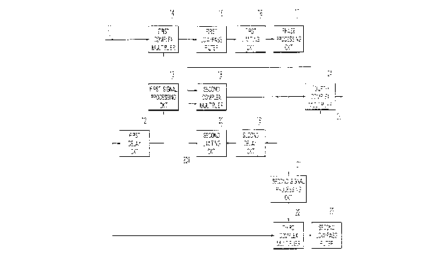
The sole figure is a block diagram of a
phase-lock loop device according to an embodiment of this
invention.
Description of the Preferred embodiment:
referring to the single figure, attention will be
directed to a phase lock loop device according to a
preferred embodiment of the present invention The
phase-locked loop device is for phase locking a device
input signal 11 representing a first complex number and
having a device input phase which should be locked into a
locked phase.
The phase-lock loop device comprises a first
delay circuit 12 supplied with the device input signal 11
for giving a delay time to the device input signal 11 and
produces a first delayed signal. The delay time is
usually represented by a complex number. The first
delayed signal has a first delayed signal amplitude and
a first delayed signal phase which is different from the
device input phase.
A first signal processing circuit 13 is connected
to the first delay circuit I The first signal
processing circuit 13 processes the first delayed signal
into a first conjugate signal representative of a first
conjugate complex number of the first complex number.
A first complex multiplier 14 is connected to the
first signal processing circuit 13 and supplied with the
device input signal 11. The first complex multiplier 14
calculates a first product of the first complex number
and the first conjugate complex number and produces a
first complex product signal representative of the first
product. The first complex product signal has a first
complex product signal amplitude.
A first low-pass filter I is connected to the
first complex multiplier 14 and filters the first complex
product signal into a first filtered signal having a
first filtered signal amplitude. A first limiting
lo circuit 16 is connected to the first-low-pass filter 15
and limits the first filtered signal amplitude to a first
limited amplitude to produce a first limited signal
having the first limited amplitude. The first limited
signal has a first limited signal phase. A phase
processing circuit 17 is connected to the first limiting
circuit 160 The phase processing circuit 17 processes
the first limited signal phase into a processed phase
which is equal to the device input phase and thereby
produces a phase processed signal representative of the
I processed phase.
second complex multiplier I is connected to
the phase processing circuit 17 and supplied with a
multiplier input signal which will presently be
described. The second complex multiplier 18 calculates a
second product of the phase processed signal and the
multiplier input signal to produce a second complex
product signal representative of the second product
representative of a second complex number.
A second delay circuit 19 is connected to the
second complex multiplier 18 and delays the second
complex product signal to produce a second delayed signal
having a second delayed signal amplitude. A second
limiting circuit 20 is connected -to the second delay
circuit 19 and limits the second delayed signal amplitude
into a second limited amplitude. The second limiting
circuit 20 supplies the second complex multiplier 18
through a delay circuit output line 201 with a second
limited signal which has the second limited amplitude and
is used as the multiplier input signal.
A second signal processing circuit 21 is
connected to the second complex multiplier circuit 18 and
processes the second complex product signal into a second
conjugate signal representative of a second conjugate
complex number of the second complex number. A third
complex multiplier 22 is connected to the second signal
processing circuit 21 and supplied with the device input
signal 11. The third complex multiplier 22 calculates a
third product of the first complex number and the second
conjugate complex number and produces a third complex
product signal representative of the third product.
A second low-pass filter 23 is connected to the
third complex multiplier 22 to filter the third complex
product signal into a second filtered signal. A fourth
complex multiplier 24 is connected to the second complex
multiplier 18 and the second low-pass filter 23. The
fourth complex multiplier 24 calculates a fourth product
of the second complex product signal and the second
filtered signal and produces a fourth complex product
signal 25 representative of the fourth product. The
fourth product signal 25 is a phase locked signal having
a fourth complex signal phase as the locked phase into
which the device input phase its locked.
The device input signal 11 is defined by a
function Us which will be represented by a polar
representation. hereunder, the polar representation will
be used in at.] equations.
Us = exit + I) + No (1)
In Equation (1), A represents an amplitude of the
device input signal 11, j represents the imaginary unit,
I represents an angular frequency, I represents a
phase angle of the device input phase, t represents time,
and No is a function which represents by the polar
representation a level of noise superposed on the device
input signal 11 at the time t.
When the device input signal 11 is sampled by a
sequence ox timing pulse signals of a sample period T, an
n-th sample value Us of an n-th sample of the device
input signal 11 is represented by:
Us = Aye To + I) + No T) (2)
Produced by the first delay circuit 12, the first
delayed signal will be represented by U12(n - Do which is
given by:
U12(n - D) = Aetna - D) + Jo i ) 3
where D represents the number of samples between the n-th
sample of the device input signal if and a delayed sample
into which the n-th sample is delayed.
Produced by the first signal processing circuit
13, the first conjugate signal will be represented by
Urn - D) which is given by:
U13(n I) = U12 (n - Do
where * represents the conjugate complex value of a
complex number.
Produced by the first complex multiplier 14, the
first complex product signal will be represented by
U14(n, D) which is given by:
U14(n; D) = Unwon - Do = Unwon D).
(3)
The device input signal Us is rewritten into:
Utah = So + No (4)
by substituting So for Aye ) ( )).
From Equations (3) and (4):
U14(n; D) = Snow - D) + Snow - D)
+ Snow - DUN + N~n)N*(n - D).
(5)
Inasmuch as the first low-pass filter 15 averages
the first complex product signal U14(n; D), each of the
second and the third terms on the right-hand side of
Equation (5! becomes equal to zero. In this event, the
fourth term on the right-hand side of Equation (5)
becomes equal to zero when the number of samples D is
large. As a result, Equation (5) is rewritten into:
U15(n - D) = Snow - D) = A2ej~(i)TD
Produced by the first limiting circuit 16, the
first limited signal wit]. be represented by U16(n - D)
which is given by:
lo ( n 5 ( n - D ) AYE = en ) TO
Produced by the phase processing circuit 17, the
phase processed signal will be represented by U17(n)
which is given by:
U17(n) = ej~(i)TD/D = exit (6)
Produced by the second complex multiplier 18, the
second complex product signal will now be assumed as:
U (n) = edgy (7)
where I represents a temporarily assumed phase which
the n-th sample of the device input signal 11 will have
in the second complex product signal.
Produced by the second delay circuit 19, the
second delayed signal will be represented by Ulg(n - 1)
which is given by:
U19(n - 1) = eon - 11
Produced by the second limiting circuit 20, the
second limited signal will be represented by U20(n - 1)
which is given by:
U20(n - 1) = ennui 1), (8)
neglecting limitation of the amplitude of the second
delayed signal.
Using Equations I and (8), the second complex
product signal U18(n) is given by:
18(n) Unwon - 1) = en IT x ennui 11
In Equation to), it will be assumed that the
number of samples D is equal to only one In this event,
the temporarily assumed phase I is represented by:
I = it + I. (9)
By using Equations (7) and (9), Equation I is
rewritten into:
ul8(n) = ej{~(i)Tn + I
= eiC')(i)Tn x eye (10)
Produced by the second signal processing circuit
21, the second conjugate signal is represented by U21(n)
which is given by:
U21(n) = U18*(n).
Produced by the complex multiplier 22, the third
complex product signal will be represented by U22(n)
which is given by:
U22(n) = Unwon = Unwon
= Aye x edgy
+ N(nT)e~j{~ To + I
Produced by the second low-pass filter 23, the
second filtered signal will be represented by U23(n)
which is given by:
U23(n) = Act (i) x e Jo. (11)
Produced by the fourth complex multiplier 24, the
fourth complex product signal will be represented by
U24(n). Using Equations (10) and (11), the fourth
complex product signal U24(n) is given by:
24 Nina = Aej~ To +
12
By comparing Equations (2) and (12~, it will be
understood that the fourth complex product phase is equal
to the device input signal phase I.
In connection with the above, the first complex
product signal Urn D) includes a desired
direct-current signal component which is represented by
the first term on the right-hand side of Equation (5).
It it possible to understand that the third complex
product signal U22(n) is another desired direct-current
signal component as a whole. Such signal components flow
through the first and the second low-pass filters 15 and
23 with no attenuation. The fourth complex multiplier 24
can therefore select the signal components embedded in
the noise superposed on the device input signal 11 and at
considerably large frequency offsets.
Thus, the illustrated example provides a powerful
tool to select a line frequency component in a phase lock
mode of operation without the phase-locking difficulties
inherent to conventional phase lock techniques.