Note: Descriptions are shown in the official language in which they were submitted.
2043325
CONTRAST CORRECTION DEVICE
The present invention relates to a television receiver
and, more particularly, to a contrast correction device which
can be used to correct contrast in a video signal in a
television receiver, a video cassette recorder, or the like.
As the screen size of colour television receivers has
increased in recent years, contrast correction devices have
become increasingly important. Such devices are used as a
means of expanding the dynamic range of the video signal
reproduced on the CRT by correcting the contrast of the video
signal for a sharper image. This has been done by passing the
video signal through a non-linear amplifier such as a gamma
correction device.
Two embodiments of known devices will be described in
detail hereinbelow.
The present invention has been developed with a view to
substantially solving the disadvantages of the prior art and
has for one object to provide an improved contrast correction
device.
In accordance with one aspect of the present invention
there is provided a contrast correction device for correcting
the contrast of an image formed by video signals by varying a
luminance signal, comprising: brightness detecting means for
detecting whether or not said image is brighter than a
predetermined brightness; and correction means for correcting
said luminance signal by a negative gamma correction when said
image is detected as brighter than said predetermined
brightness, whereby contrast of bright image areas in said
image are enhanced.
~'
2 2043325
In accordance with another aspect of the present
invention the above described contrast correction device
further includes darkness detecting means for detecting
whether or not said image is darker than a predetermined
darkness; and correction means for correcting a luminance
signal by a positive gamma correction when said image is
detected as darker than said predetermined darkness, whereby
contrast of bright image areas in said image are suppressed.
In accordance with yet another aspect of the present
invention there is provided a contrast correction device for
correcting the contrast of an image formed by video signals by
varying a luminance signal, comprising: brightness/darkness
detect-ing means for detecting a tone level of said image and
for producing a bright signal when said tone level is greater
than a predetermined brightness, and a dark signal when said
tone level is less than a predetermined darkness; and
correction means for correcting said luminance signal by a
negative gamma correction in response to said bright signal,
and a positive gamma correction in response to said dark
signal, whereby contrast of bright image areas in said image
are enhanced when said bright signal is produced, and the same
are suppressed when said dark signal is produced.
The present invention will be described in detail
hereinbelow with the aid of the accompanying drawings, in
which:
Fig. 1 is a block diagram of a contrast correction device
according to a first embodiment of the present invention;
Fig. 2 is a block diagram of a positive/negative gamma
correction circuit shown in Fig. 1;
Fig. 3 is a graph showing waveforms of signals observed
at various places in the contrast correction device shown in
Fig. 2;
Fig. 4 is a block diagram of a contrast correction device
according to a second embodiment of the present invention;
.~
3 2043325
Figs. 5a, 5b, 5c, 5d, and 5e are graphs showing the
input-output characteristics observed in various conditions;
Fig. 6 is a block diagram of a first example of a
conventional contrast correction device;
Figs. 7a and 7b are graphs showing the input-output
characteristics observed in the contrast correction device
shown in Fig. 6;
Fig. 8 is a block diagram of a second example of a
conventional contrast correction device; and
Fig. 9a and 9b are graphs showing the input-output
characteristics observed in the contrast correction device
shown in Fig. 8.
It should be noted that throughout this description like
parts are designated by like reference numerals.
Figs. 6, 7a and 7b are, respectively, a block diagram and
graphs showing the input/output relationship in a first
example of a conventional contrast correction device.
As shown in Fig. 6, the contrast correction device
comprises a gamma correction circuit 1 which corrects the
luminance signal S1 input thereto. Gamma correction device 1
suppresses white or bright tones according to an average
detected luminance signal S3'. The circuit includes an
average luminance detection circuit 2 which averages the
~ nce signal S2' over one or a plurality of frames and
produces an average detected luminance signal S3'. A matrix
circuit 3 adds the luminance signal S2' and an input colour
difference signal S4 to output the colour signal S5' to a CRT
4. A contrast correction device thus constructed operates as
described below.
First, the post-correction luminance signal S2' is input
to the average luminance detection circuit 2 for averaging the
signal S2' over a predetermined time which may be more than
one vertical scan period to detect the average luminance
signal S3'. The detected average luminance signal S3' is
4 2043325
input to the gamma correction circuit 1. The gamma correction
circuit 1 changes the input-output characteristics according
to the average detected luminance signal S3' as shown in
Figs. 7a and 7b.
More specifically, when the average detected luminance
signal S3' is of a dark image, white or light tones are
suppressed and black tones are enhanced as shown in Fig. 7a.
On the contrary, when the average detected luminance signal
S3' is of a bright image, suppression of white or light tones
is weakened as shown in Fig. 7b, so that white or light tones
are enhanced more than that resulting from the case shown in
Fig. 7a. The post-correction luminance signal S2' thus
obtained is input to the matrix circuit 3 to be added with the
input colour difference signal S4, resulting in the generation
of the colour signal S5' to drive the CRT 4 to generate the
vldeo image.
Figs. 8, 9a and 9b are, respectively, a block diagram and
graphs showing the input-output characteristics according to a
second example of a conventional contrast correction device.
When compared with the example shown in Fig. 6, the
contrast correction device shown in Fig. 8 has, in place of
the average luminance detection circuit 2, a white peak level
detection circuit 6 which detects the whitest level of the
post-correction luminance signal S2" and outputs a white peak
signal S6'. A white peak comparison circuit 7 is included
which compares the white peak detection signal S6' with a
predetermined white peak level signal Vg' which is set
externally. Comparison circuit 7 outputs the result as a
white peak comparison signal S8'.
The contrast correction device of Fig. 8 operates as
described below.
First, the post-correction luminance signal S2' is input
to the white peak level detection circuit 6 to detect the
white peak level (the luminance of the whitest part of the
video signal) over a predetermined time which may be more than
one vertical scan period. The detected white peak level is
output as the white peak detection signal S6' (the level of
~ .~
2043325
which increases as the white peak level increases) and is
compared by the white peak comparison circuit 7 with an
externally set white peak level voltage Vg', thus yielding the
white peak comparison signal S8', which is input to the gamma
correction circuit 1. The gamma correction circuit 1 changes
the input-output characteristics as shown in Figs. 9a and 9b
according to the white peak comparison signal S8'. When the
voltage level of the white peak level voltage Vg' is equal to
or greater than the white peak detection signal S6' (i.e.,
when the image is dark overall), the light tones are
suppressed as shown in Fig. 9a to enhance the dark tones.
When the white peak level voltage Vg' is less than the white
peak detection signal S6' (i.e., when the image is bright
overall), correction is suppressed as shown in Fig. 8b for
better enhancement of the light tones when compared with
Fig. 9a. The post-correction luminance signal S2' thus
obtained, is input to the matrix circuit 3 where it is added
to the input colour difference signal d to generate the colour
signal S5", which is then used to drive the CRT 4 to generate
the video image.
However, with conventional contrast correction devices as
described above, when the average luminance is bright in the
first example, or the white peak detection signal S6' level is
high (bright) in the second example, the gamma input-output
characteristics of light or white tones are simply made
approximately linear. This does not make it possible to
expand the dynamic range, resulting in the need to further
expand the dynamic range to achieve a high image quality in
large-screen television displays.
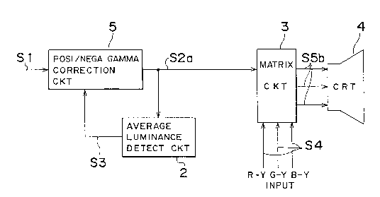
First Embodiment
Referring to Fig. 1, a contrast correction device
according to a first embodiment of the present invention is
shown. The contrast correction device comprises a
positive/negative gamma correction circuit 5 for correcting
the luminance signal Sl according to the average luminance
6 2043325
signal S3 as described below. When the average luminance
signal S3 is relatively low indicating that the image is dark,
the positive gamma correction characteristics are applied for
contrast correction whereby the contrast of light or white
tones in the luminance signal Sl is suppressed for the better
enhancement of dark tones. When the average detected
luminance signal S3 is bright, negative gamma correction
characteristics are applied for contrast correction whereby
the contrast of light tones is enhanced as will be described
in detail later. The average luminance detection circuit 2,
matrix circuit 3, and CRT 4 are the same as those used in the
conventional contrast correction device described hereinabove.
The average luminance detection circuit 2 receives the post-
correction signal S2 and takes an average over one or a number
of frames to produce an average luminance signal S3 as shown
in Figs. 5a to 5e. The average luminance signal S3 is then
input to the positive/negative gamma correction circuit 5.
When the detected average luminance is low (dark), such
as in the case of Fig. 5e, the average luminance signal S3
will be relatively low, such as -C in which C=1 according to
the present embodiment. In response to signal S3, which is
-C in this case, the positive gamma correction is carried out
in the positive/negative gamma correction circuit 5 so as to
establish the input/output characteristics of the gamma
correction circuit 5 that bends downward as shown in Fig. 5e,
in a manner which will be described in detail later. Thus the
contrast of bright (white) tone areas is suppressed for the
better enhancement of the dark tone areas.
When the detected average luminance is a medium contrast,
such as in the case of Fig. 5c, the average luminance signal
S3 will take an intermediate level, such as 0. In response to
signal S3, which is 0 in this case, no gamma correction is
carried out in the positive/negative gamma correction circuit
5 so as to establish the input/output characteristics of the
gamma correction circuit 5 that extends straight as shown in
Fig. 5c. When the detected average luminance is high (bright)
such as in the case of Fig. 5a, the average luminance signal
7 2043325
S3 will be relatively high, such as +C. In response to signal
S3, which is +C in this case, the negative gamma correction is
carried out in the positive/negative gamma correction circuit
5 so as to establish the input/output characteristics of the
gamma correction circuit 5 that bends upward as shown in
Fig. 7a. Thus the contrast of light (white) tone areas is
enhanced.
When the detected average luminance is slightly low or
slightly high, the average luminance signal S3 will be at
corresponding levels, such as -0.5C or +0.5C, as shown in
Figs. 5d or 5b, respectively. In such cases, the input/output
characteristics of the correction circuit 5 will be slightly
bent upwards or downwards as shown in Figs. 5d and 5b,
respectively.
Referring to Fig. 2, a detailed block diagram of the
positive/negative gamma correction circuit 5 is shown.
The luminance signal S1 is shown as a waveform of negative
going signal. The positive/negative gamma correction circuit
5 comprises one or more, such as three in the example shown in
Fig. 2, comparator circuits 9a, 9b, and 9c, and a voltage
divider defined by a plurality of resistors connected in
series between a line carrying pedestal voltage Vj and a line
carrying white peak voltage Vk to produce reference voltages
Vq, Vr and Vs. Note that Vq<Vr<Vs. Comparator circuit 9a
compares the input luminance signal S1 with the predetermined
reference voltage Vq which is between voltages Vj and Vk and
produces an output se corresponding to a portion of the input
luminance signal Sl that has exceeded the reference voltage
Vq, as shown in Fig. 3. Similarly, comparator circuit 9b
produces an output Sm corresponding to a portion of the input
luminance signal Sl that has exceeded the reference voltage Vr
and comparator circuit 9c produces an output Sn corresponding
to a portion of the input luminance signal Sl that has
exceeded the reference voltage Vs. An adder 10 is provided
for adding the compared luminance signals SQ, Sm, and Sn to
produce a correction signal So, as shown in Fig. 3.
,~
~L
8 2043325
The correction signal So is amplified in a gain control
circuit 11, the gain of which is controlled by the average
luminance signal S3 to be between -C and +C. Thus, gain
control circuit 11 produces a control correction signal Sp, as
shown in Fig. 3, in which the solid line is obtained when
S3=+C, the dotted line is obtained when S3=-C, and the dot-
dash line is obtained when S3=0. An adder circuit 12 then
adds the control correction signal Sp and luminance signal Sl
to produce the post-correction luminance signal S2a, which is
also shown in three different conditions using a solid line, a
dotted line and a dot-dash line. The dotted line corresponds
to the case shown in Fig. 5e in which the positive gamma
correction is obtained; the solid line corresponds to the case
shown in Fig. 5a in which the negative gamma correction is
obtained; and the dot-dash line corresponds to the case shown
in Fig. 5c in which no gamma correction is obtained. It is to
be noted that negative gamma input-output characteristics are
obtained when the gain of the gain control circuit 11 is
negative, and positive gamma input-output characteristics are
obtained when the gain is positive. In the present
embodiment, the input-output characteristics are varied by the
use of three comparator circuits 9a, 9b and 9c, but the number
of comparator circuits may be any other number greater than
one.
According to the contrast correction device of the
present embodiment, it is possible to obtain positive gamma
input-output characteristics when the average value is dark
and negative gamma input-output characteristics when the
average value is bright. Thus, when the averaged brightness
level of one or several image frames has a relatively high
level, the contrast of the light tone areas will be enhanced.
On the other hand, when the average brightness level of one or
several image frames has a relatively low level, the contrast
of the dark tone areas will be enhanced.
"~ ",
9 2 0 ~ 2 ~
Second Embodiment
Referring to Fig. 4, a block diagram of a contrast
correction device according to a second embodiment of the
present invention is shown. According to the second
embodiment, the average luminance detecting circuit 2 is
replaced with a white peak level detection circuit 6 which
produces a white peak detection signal S6 as shown in
Figs. 5a-Se. The white peak detection signal S6 is compared
in a comparator 8 with a high threshold voltage VH and a low
threshold voltage VL.
When the white peak detection signal S6 is greater than
the high threshold voltage VL, a signal S8 produced from
comparator 8 is in a high level, such as +C. The negative
gamma input-output characteristics are established in the
positive/negative gamma correction circuit 5 in a similar
manner described above. This condition is shown in Fig. 5a.
When the white peak detection signal S6 is smaller than
the low threshold voltage VL, the signal S8 from comparator 8
is in a low level, such as -C. The negative gamma input-
output characteristics are established in thepositive/negative gamma correction circuit 5 in a similar
manner described above. This condition is shown in Fig. 5e.
When the white peak detection signal S6 is between the high
and low threshold voltages VH and VL, the signal S8 from
comparator 8 is in an intermediate level, such as 0. Thus, no
gamma correction is added to the characteristic line in the
positive/negative gamma correction circuit 5. This condition
is shown in Fig. 5c. In other words, according to the second
embodiment, when the white peak detection signal S6 is smaller
than the low threshold VL, (i.e., when the image itself is
considered to be dark), the contrast of light or white tone
areas is suppressed for the better enhancement of dark tone
areas as shown in Fig. 5e. When the white peak detection
signal S6 is between the low and high thresholds VL and VH, a
f~
lO 2043325
linear characteristic is applied as shown in Fig. 5c. When
the white peak detection signal S6 is greater than the high
threshold VH (i.e., when the image itself is considered to be
bright), the contrast of light tone areas is enhanced as shown
in Fig. 5a.
Thus, the contrast of light tone areas (dynamic range)
can be extended by suppressing the contrast of light or white
tone areas to enhance the contrast of dark tone areas when the
white peak level is low (dark), and enhancing the contrast of
light or white tone areas when the white peak level is
relatively high (bright).
It is to be noted that in the first embodiment of the
present invention the input signal to the average luminance
detection circuit 2 is the post-correction luminance signal
S2b, but the luminance signal Sl may also be input thereto.
Furthermore, in the second embodiment of the present
invention the input signal of the white peak level detection
circuit 6 is the post-correction luminance signal S2b, but the
luminance signal Sl may also be input thereto.
According to the contrast correction device it is
possible to extend the dynamic range of a video signal on the
white contrast region by providing a positive/negative gamma
correction circuit in the contrast correction device.
It is more effective to provide a gain control device in
a stage before the positive/negative gamma correction circuit
5 so as to control the rising angle e of input-output
characteristics line relative to the darkness of the image.
-