Note: Descriptions are shown in the official language in which they were submitted.
;~043545
SPECIFICATION
Title of th~. Inv~-n~inn
PROCESS FOR PREPARING S~JPERCONDUCTING JUNCI'ION
OF OXIDE SUPERCONDUCTOR
R~ ln~l of tllP. Iny~ntion
Fi~ld of ~h~ jn~fenti~n
The present invention relates to a process for preparing
superconducting junctions of oxide superconductor such as Josephson
Junction, more particularly to a process for preparing a superconducting
junction by depositing successively a first oxide superconductor thin film
layer, a non-superconducting interme~ te thin film layer and a second
oxide superconductor thin film layer on a substrate in this order.
1 5
pesc~tion of th~ related art
In order to realize electronics devices such as Josephson element or
superconducting transistors in which superconductor is combined with
semiconductor, it is indispensable to deposit successively at least one thin
film layer of superconductor and at least one thin fi~m layer of non-
superconductor on a substrate. Hereinafter, we will describe the present
invention with reference to Josephson junction used for fabricating
Josephson element but it is apparent that the process according to the
present invention is applicable to the other type superconducting devices.
2 5 A variations of Josephson Junctions have been reported. Among
them, the most simplest type is so-called tunnel Josephson Junction in
which a non-superconducting ~hin film layer is sandwiched between a pair
2~3545
of superconductors. Tunnel type Josephson element is fabricated by
processing microscopically a layered structure of 1st superconductor thin
film layer/non-superconductor thin film layer/2nd superconductor thin
film layer. In thi~ Josephson Junction, thickness of the inte~nediate thin
S fi~n layer of non-superconducting is determined by ~e coherent length of
superconductors .
Although several ideas for fabricating the tunnel type
superconducting junctions from metallic superconductors have been
reported, there is little report describing how to fabricate the same from
10 oxide superconductors because there remain following problems to be
solved in order to prepare the tunnel type superconducting junctions
having oxide superconductor ~hin ~llrn layers.
Firstly, in the case of tunnel type superconducting junctions having
oxide superconductor thin film layers, the thickness of non-
15 superconducting intermediate thin film layer must be reduced to severalnanometers (nm) because of very short coherent length of oxide
superconductor.
Secondly, it is difficult to deposit and/or l~min~te oxide thin films
having good crystallinity successively. In particul~r, in the prior art, it is
2 0 difficult to prepare an upper superconductor thin film layer having good
crystallinity on a non-superconducting interme~ te thin f11m layer due to
very poor crystallinity of the later layer. In order to improve
performance of superconducting thin film devices, it is preferable ~at all
thin film layers are made of single crystals. In fact, if any one of the
2 5 layers is of a polycrystal or amorphous film, the tunnel type Josephson
Junction doesn't work stably. In other words, there is a strong dernand to
prepare the second or upper superconductor thin film layer of single
20435
crystal having good crystallinity on a non-superconducting intermediate
layer. Deposition of oxide superconductor thin film layer of single
crystal having good crystallinity is requested also in the field of
superconducting transistor having an interface between oxide
5 superconductor and semiconductor.
In fact, tunnel type superconducting junctions prepared from oxide
superconductor by the conventional technique did not show desired
electrical properties due to poor interface condition between the oxide
superconductor thin film layer and the non-superconductor thin film
1 0 layer.
Therefore, an object of the present invention is to solve the
problems and to provide a process for improving crystallinity of the non-
superconducting intermediate thin film layer and hence the second or
upper superconducting thin film layer in order to permit high-
1 5 temperature superconductors to be utilized in actual uses.
Summary of the Invention
The present invention provides a process for fabricating asuperconducting junction by depositing successively a first oxide
2 0 superconductor thin film layer, a non-superconducting intermediate thin
film layer and a second oxide superconductor thin film layer on a
substrate in this order, characterized in that the non-superconducting
intermediate thin film layer is composed of MgO and in that said substrate
is heated at a temperature between 200 and 400 C during deposition of the
2 5 non-superconducting intermediate thin film layer.
~ _,
2~4~545
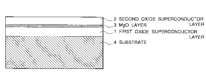
Brief Description of the Drawin~
Fig. 1 is a diagrammatical cross sectional view of a product
obtained by the process according to the present invention.
Fig. 2A and 2B are photos taken by a scanning electron
5 spectroscopy (SEM) on cross sections of products prepared in Example 1
according to the present invention.
Fig. 3 illustrates substrate temperature dependency of surface
roughness and of crystal orientation in an intermediate thin film layer of
MgO deposited on a first oxide superconducting thin film layer of
1 o Y1Ba2Cu3O7 x prepared in Example 3 according to the present invention.
As is illustrated in Fig. 1, the superconducting junction prepared by
the process according to the present invention has a layered structure
consisting of a first oxide superconductor thin film layer (1), a non-
15 superconducting intermediate thin film layer (3) and a second oxidesuperconductor thin film layer (2) deposited on a substrate (4) in this
order.
The first feature of the present invention reside in that the substrate
is heated at a temperature between 200 and 400 C during the non-
-4 -
~5' ~"
Z0435AS
superconducting intermediate thin film layer of MgO is deposited. If the
substrate temperature is not heated higher than 200 ~C, the resulting thin
~llm layer of MgO possesses poor crystallinity or becomes amorphous.
To the contrary, if the substrate temperature is heated above 400 C, the
S resulting thin film layer of MgO becomes polycrystal. In both cases, no
desired superconducting junction can not be obt~ine~
Thickness of the ~IgO thin film layer is also important in the
process according to the present invention and is preferably between 1
and 10 nm. If ~e thic~cness of ~e MgO thin film layer is not thicker than
10 1 nm, it is difficult to forrn a uniform thin film of MgO and the
crystallinity of the thin film become poor. To the contrary, if the
thickness of MgO thin film layer exceed 10 nm, it is also difficult to
deposit a well-ordered second superconductor thin film layer thereon
because the crystallinity of MgO thin film layer is disturbed and a desired
1 5 coherent length can not be obtained.
All of the first and second oxide superconductor thin film layers
and the non-superconducting intermediate thin ~llm layer can be prepared
by any known technique but are prepared preferably by physical vapour
deposition method including sputtering rnethod, vacuum evaporation
2 0 method and molecular beam epitaxy method. Chemical vapour deposition
method also may be used.
In a preferred embodiment of the present invention, the ~lrst oxide
superconductor thin film layer is prepared by sputtering, vacuum
evaporation and molecular beam epitaxy and both of the non-
25 superconducting intermediate thin filn~ layer and the second oxidesuperconductor thin film layer are prepared by vacuum evaporation
method which give no bad influen&e to an under-layer.
-5-
Z043545
The second feature of the present invention res~de in that the
orientation directions of the first and second superconducting thin fil
layers can be made identical to each other. In fact, when the first
superconducting thin film layer is a c-axis oriented film, the second
5 superconducting ~in film layer deposited thereon becomes also a c-axis
oriented film, and, when the first superconducting thin film layer is an a-
axis oriented ~llrn, the second superconducting thin film layer deposited
thereon becomes also an a-axis onented film. Selection of orientation can
be made according to applications. Orient~tion of superconducting thin
1 O film ]ayers can be changed by controlling the substrate temperature
during deposition. For example, in the case of a thin film layer of Y-Ba-
Cu O system deposited on a single crystal of MgO (100~ by sputtering
method, c-axis oriented superconducting thin film is obtained at a
substrate temperature of 630 C, while a-axis oriented superconducting
1 5 thin film is obtained at a substrate te~ ~ture of 600 C.
The first and second oxide superconductor thin film layers are
preferably made of a compound oxide selected from the group
comprising Y-Ba-Cu-O system such as YIBa2cu3o7-x~ Bi-Sr-Ca-Cu-O
system such as Bi2Sr2Ca2Cu30x and Tl-Ba-Ca-Cu-O system such as
2 0 T12Ba2Ca2CU3x YlBa2cu3o7-x is preferable because ~hin films of high
quality are obtainable stably and T12Ba2Ca2Cu30x is also preferable due
to its high critical temperature (Tc).
The substrate is not limited but is preferably a single crystal
substrate of oxide such as MgO, SrTiO3, LaA103, LaGaO3 and yttriun
2 ~ stabilized zirconia (YSZ). The ~Irst oxide superconductor thin ~llm layer
is deposited preferably on a (100) plane of a single crystal substrate of
MgO.
2043S45
In a preferred embodiment according to ~he present invention~ the
substrate on which the first oxide superconductor thin film layer has been
deposited previously is hea~ed at a temperature between 600 and 650 C,
before and the non-superconducting intermediate thin film layer is
5 deposited. By this heat-treatment, a surface of the thin film layer of MgO
is cleaned and the quality of the second superconducting thin ~lm layer is
improved.
This heat-treatment is effected preferably in oxygen containing
atmosphere.
Inventors of this application found that this technique is not limited
to the thin film layer of MgC) but is applicable to the other non-
superconducting intermediate layers such as SrTiO3, LaA103 or LaGaO3.
In particular, this heat-treatment technique is advantageous in such a
case when the intermediate layer is prepared by a different method from
that is used for depositing the first superconducting thin film layer. For
example, when first superconducting thin film layer is prepared by
sputtering method while the interme~ te layer and/or the second
superconducting thin film layer are prepared by vacuum evaporation
method, a substr~té on which first superconducting thin film layer is
deposited is transferred from a chamber of sputtering unit to another
chamber of vacuum evaporation unit. The surface of thc first
superconducting thin film layer is exposed to atmosphere and may be
deteriorated during the transfer. Such spoiled surface can be cleaned by
the heat-treatment technique according to the present invention.
When a temperature of this heat-treatment is not higher than
600 3C, effective cleaning can not be expected. To the contrary, if the
temperature of this heat-treatment exceeds over 650 C, the first
;.
Z(~43545
superconducting thin film layer is deterior~ted due ~o migration of
substrate material into the superconducting thin film layer and
recrystallization of the later. This heat-treatment is preferably carried
out for more than S minutes.
S The other operational condition ex&ept the temperature during the
heat-treatment can be identical with those used in the above-mentioned
case.
Ln conclusion, the process acc~rding to the present invention has
following advantages:
(1) A thin fi]m of high quality can be deposited on an oxide
superconducting thin film layer.
(2) Tunnel type superconducting junction which is an indispensable
element for realizing el~ctronics devices can be obtained.
(3) Orientation of crystals can be controlled freely, so that the critical
current density can be flown in parallel with (c-axis oriented ~llm)
or perpendicular to (a-axis oriented film) a surface of the substrate.
Descr~tion of ~h~ Preferred F~Jnbodin~nts
Now, the present invention will ~e described with reference to
2 0 Examples, but the scope of the present invention should not be limited
thereto.
Fx~ le 1
A first, a superconducting thin film layer having a composition of
2 5 YlBa2Cu307 x was deposited on a (100) plane of a MgO single cIystal by
RF-magnetron sputtering.
_~9
204~545
In this Example, both of c-axis oriented and a-axis oriented thin
films of superconductors of YlBa2Cu307 x were prepared by changing
the substrate temperature.
Essential operational conditions used for preparing thc ~lrst o~ide
5 superconducting thin film layer are as foIlowing:
Substrate temperature: 630 C for c-a~is oriented film
~00 C for a-axis oriented ~llm
Sputtering gas: Ar: 8 sccm
2: 4 sccm
I O Gaspressure: 5 ~ 10-2 Torr
Thickness of 1 st layer: 300 nm
The resulting substrate having the first oxide superconducting thin
film layer was transferred from a sputtering chamber to a vacuum
evaporation chamber and then a non-superconducting intermediate thin
film layer of MgO was deposited on the first oxide superconducting thin
film layer by vacuum evaporation method. Essential operational
conditions used for preparing the MgO layer are as following:
Substrate temperature: 400 C
Gas pressure: 4 x 10⁻⁴ Torr
2 0 Thickness of MgO: S nm
Then, in the same chamber, a second oxide superconducting thin
film layer of YlBa2Cu307 x was deposited on the resulting MgO thin film
layer by vacuum deposition method. F.ssenti~l operational conditions used
for preparing the 2nd layer are as following:
2 5 Substrate temperature: 630 C
Gas pressure: 4 x 1~4 Torr
Thickness of 2nd layer: 200 nm
g
Z043545
It was confirmed, by a sc~nning electron microscopy (SEM), such a
fact that, when the first oxide superconducting thin film layer was a c-axis
oriented film of YlBa2Cu307.x, the second oxide supercor~cting thin
film layer deposited thereon through MgO thin film layer bec~me also a
S c-axis oriented film of Y1Ba2Cu3O7 x, and, when the firs~ oxide
superconducting thin ~llm layer was an a-axis oriented film, ~e second
oxide superconducting thin film layer deposited thereon through MgO
thin fillTI layer became also an a-axis oAented film.
Fig. 2A is a photo taken by a sc-~nning electron spectroscopy tSEM)
on a cross section of the resulting layered structure Of YlBa2cu3o7-x /
MgO / Y1Ba2Cu3O7 x in which both of the 1st and 2nd oxide
superconducting thin film ]ayers were c-axis oriented ~llms.
Fig. 2B is a photo taken by a scarming electron spectroscopy (SEM)
on a cross section of the resulting layered structure of YlBa2Cu307 x /
MgO / YlBa2Cu3O7 x in which both of the 1st and 2nd oxide
superconducting thin film layers were a-axis oriented films.
Fig. 2A and 2B reveal such facts that crystals of YlBa2Cu307 x in
the first and second oxide superconducting thin film layers were oriented
along an identical direction in the superconducting junctions prepared by
the process according to the present invention and that an interface
between MgO intermediate thin film layer and firsttsecond oxide
superconducting thin film layer is very sharp and has so serious disorder.
Fx~le ~
2 5 The same procedure as Example 1 was repeated but first/second
oxide superconducting thin film layers of YIBa2Cu307 x were replaced
by Bi2sr2ca2cu3ox-
- 10-
20435~5
Essential operational conditions used for preparing the ~Irst oxide
superconducting thin film layer are as following:
Substrate temperature: 660 C for c-axis oriented
630 C for a-axis oriented
Sputteringgas: Ar: 8 sccm
2: 4 sccm
Gas pressure: 5 x 1~2 Tor,r
l'hickness of 1 st layer: 300 nm
Essential operational conditions used for preparing the MgO layer
are as following:
Substrate temperature: 400 C
Gas pressure: 4 x 10⁻⁴ Torr
Thickness of MgO: S nm
Then, in the same chamber, a second oxide superconducting thin
film layer of Bi2Sr2Ca2Cu3Ox was deposited on the resulting MgO thin
film layer by vacuum deposition method. Essential operational conditions
used for preparing the 2nd layer are as following:
Substrate temperature: 660 C
Gas pressure: 4 x 10⁻⁴ Torr
2 0 Thickness of 2nd layer: 200 nm
Jn this Example also, it was confirmed, by a scanning electron
microscopy (SEM), SUC~l facts that, when the first oxide superconducting
thin film layer was a c-axis oriented film of Bi2Sr2Ca2Cu30x, the second
oxide superconducting thin film layer deposited thereon Ihrough hIgO
2 5 thin film layer became also a c-axis oriented film of Bi2Sr2Ca2Cu3Ox,
and, when the first oxide superconducting thin fi~n layer was an a-axis
oriented film, the second oxide supercon~ ctin~ thin film layer deposited
- 1 1 -
2043545
thereon through MgO thin film layer ~ec~me also an a-axis oriented film
and that crystals of Bi2Sr2Ca2Cu30x in the first and second oxide
superconducting thin f;lm layers were oriented along an identical
direction in the superconducting junctions and also that an interface
S between MgO intermediate thin film layer and first/second oxide
superconducting thin film layer was very shaIp and had so serious
disorder.
E~AtnP1e 3
The same procedure as Example 1 was repeated but the substrate
temperature for depositing the intermediate thin film layer of MgO was
modified.
The results are summarized in Fig. 3 which illustrates substrate
temperature dependency of surface roughness and of crystal orientation in
l S an intermediate thin film layer of MgO deposited on a first oxide
superconducting thin film layer of YlBa2cu3o7-x.
Fig. 3 reveals such a fact that intermediate non-superconducting
thin film layers of MgO deposited on the first oxide superconducting thin
film layer of YlBa2Cu307 x show uneven or rough surface at substrate
2 0 temperatures of higher than 400 C and become amolphous at substrate
temperatures of lower than 200 C.
Pig. 3 revea]s such a fact also that the intel.l.ediate non-
superconducting thin film layers of M~O contains (110) plane on its
surface on which the second superconducting thin film layer will be
25 deposited, in addition to (100) plane. ~uch mixed planes result in
deterioration of crystallinity.
- 12 -
~043545
From the result, it was confirmed that it is indispensable to limit the
substrate temperature between 200 C and 400 C in order to realize a
smooth (100) plane possessing improved crystallinity which is an
indispensable condition to produce the second oxide superconducting thin
5 film layer having the same deposition plane as the ~Irst oxide
superconducting thin film layer.
F.~ample 4
In this Example, a first oxide superconducting thin film layer was
10 heat-treated previously before an intennedi~te non-superconducting thin
film layer was deposited.
A first, a superconducting thin film layer having a composition of
YlBa2Cu307 x was deposited on a (100) plane of a ~IgO single clystal by
RF-magnetron sputtering.
Essential operational conditions used for preparing the first oxide
superconducting thin film layer are as following:
Substrate temperature: 630 C for c-axis oriented film
Sputtering gas: Ar: 8 sccm
2: 4 sccm
2 0 Gas pressure: 5 x lo-2 Torr
Thickness of 1 st Iayer: 300 nm
The resulting substrate having the ~l~st oxide superconducting thin
film layer was transferred from a sputtering chamber to a vacuum
evaporation chamber.
2 5 In the vacuum evaporation cham~er, the heat-treatment was effected
with supplying oxygen gas through a nozzle onto a surface of the substrate
for 30 minutes, under following condition:
204~545
Substrate temperature: 600 C for c-axis oriented fiLm
Surrounding gas: 2
Gas pressur~: 4 x 10⁻⁴ Torr
(This value is a pressur~ in the vacuum evaporation chamber
S but is not a pressure around the substrate where gas pressure
may be one to two orders (10-3 to 10-2) higher than this
value)
Then, the substrate was left to be cooled down to 40~ C.
After then, a non-superconducting intermediate thin film layer of
MgO was deposited on the heat-treated first oxide superconducting thin
film layer by vacuum evaporation method. Essential operational
conditions used for preparing the MgO layer are as following:
Substrate temperature: 400 C
Gas pressure: 4 x 10⁻⁴ Torr
1 5 Thickness of MgO: 5 nm
Then, in the same cham~er, a second oxide superconducting thin
film layer of YlBa2Cu307 x was deposited on the resulting MgO thin ~
layer by vacuum deposition method. Essential operational conditions used
for preparing the 2nd layer are as following:
2 0 Substrate temperature: 630 C
Gas pressure: 4 x 1 0-4 Torr
Thickness of 2nd layer: 200 nm
By a scanning electron microscopy (SEM), it was con~lrmed such
facts that an interface between MgO inte-mediate thin film layer and
2 5 firstlsecond oxide superconducting thin film layer was very sharp and that
disorder of crystals at the interface was less ~an 1 nm in width.
2043545
In a comparative example which was not subjected to the heat-
treatrnent, disorder of ~rystals in width at ~e interface of S to 10 nm was
observed.
F,~ le 5
The same procedure as Example 4 was repeated but first/second
oxide superconducting thin film layers of YlBa2Cu307 x were replaced
by Bi2sr2ca2cu3ox-
Essential operational conditions used ~or preparing the first oxide
10 superconducting thin film layer are as fo~lowing:
Substrate temperature: 660 C for c-axis oriented film
Sputtering gas: Ar: 8 sccm
2: 4 sccm
Gas pressure: 5 x lO-2 Torr
1 5 Thickness of I st ]ayer: 300nm
Heat-treatment was effected for 30 minutes under following cond~tions:
Substrate temperature: 600 C for c-axis oriented film
Surrounding gas: 2
Gas pressure: 4 x 10⁻⁴ Torr
2 0 Essential operational conditions used for preparing the MgC) layer are as following:
Substrate temperature: 400 C
Gas pressure . 4 x 10⁻⁴ Torr
Thickness of MgO: 5 nm
2 5 Then, in the sarne chamber, a second oxide superconducting thin
film layer of Bi2Sr2Ca2Cu30x was deposited on the resulting MgO thin
2043545
film layer by vacuum deposition me~od. Essential operational conditions
used for preparing the 2nd layer are as following:
Substrate temperature: 650 ~C
Gas pressure: 4 x 10⁻⁴ Torr
Thickness of 2nd layer: 300nm
By a scanning e]ectron microscopy (SEM), it was confilmed such
facts that an interface between MgO intermediate thin film layer and
~lrst/second oxide superconducting thin film layer was very sharp and that
no substantial disorder of crystals at the interface was observed.
In a comparative example which was not subjected to the heat-
treatment, disorder of crystals in width at the interface of S to 10 nm was
observed.
F.x~n~le 6
The same procedure as Example 4 was repeated but non-
superconducting ~in film of MgO was replaced by SrTiO3 and deposition
of this non-superconducting thin film of SrTiO3 was effected under
following conditions:
Substrate temperature: 610 C
2 0 Gas pressure: 4 x l~4 Torr
Thickness of SrTiO3: 5 nrn
By a scanning electron microscopy ~SEM), it was confirmed such
facts that an interface between SrTiO3 intennediate thin film layer and
first/second oxide superconducting thin film layer was very sharp and that
2 5 disorder of crystals at the interface was less than 1 nm in wid~.
- 1 6 -