Note: Descriptions are shown in the official language in which they were submitted.
` 1 20'~3~9S.
TITLE OF THE INVENTION
OPTICAL TRANSCEIVER
BACKGROUND OF THE INVENTION
The present invention relates to an optical
transceiver which is provided at each terminal in a data
communication system employing a pair of optical data
buses which are of such a linear bus type as an optical
data bus for aircraft and transmit optical signals in
opposite directions.
In general, a linear bus system is used as one
method for forming an optical data bus. In the linear
bus system a plurality of terminals are connected to a
plurality of optical couplers inserted in an optical data
bus, and hence are linearly arranged and connected
(without forming loops or stars). Since the optical
coupler is directional, however, two optical data buses
are needed for transmission and reception between
terminals. Accordingly, each terminal has two systems
of optical transceivers so that it is capable of
transmission and reception over either of the two optical
data buses.
A description will be given first, with reference
to Fig. 1, of a conventional linear bus type optical data
communication system. Each terminal equipment TEi (i =
1, 2, ...) is connected via optical couplers C1 and C2
to a linear bus type first optical data bus L1 for
transmission in a first direction A and a linear bus type
second optical data bus L2 for transmission in a second
direction B opposite to the first direction A. The
terminal equipment TEi comprises an optical transceiver
PTi connected to the optical couplers C1 and C2 via
transmitting optical fibers FT1 and FT2 and receiving
optical fibers FR1 and FR2, a bus controller BCi for
.~
20~3596
contI;ollin~ c~mtllunica~ion3, nlld n ~n~ r~ l DT~ r~I
transmitting and receiving data. The terminal equipment
TEi provides an optical data signal on the optical data
buses Ll and L2 and receives an opticàl data signal
therefrom. Each terminal equipment TEi delivers the
optical data signal, using a different time slot so that
the optical data signal will not interfere with those
from other terminal equipment. Thc bus controller BCi
receives the data transmitted from the terminal equipment
TEi so as to see if the t,ransmitted and the received data
do not coincide, and if not, the bus controller BCi will
judge that an abnormality is present in any one of the
transmitting and receiving routes such as the optical
fibers FTl, FT2, FRl and FR2, and the optical couplers
Cl and C2. The bus controller BCi, which controls
communications between data terminals DTi according to
predetermined rules, is connected to a data input/output
end of each data terminal DTi. The optical transceiver
PTi is connected between the bus controller BCi and the
corresponding optical couplers C1 and C2. Transmission
data SD input from the bus controller BCi into the
optical transceiver PTi is supplied in parallel to
transmitting circuits Tl and T2 and, after being
modulated, they are supplied to light emitting elements
(LED's, for example) LEl and LE2, wherein they are
converted to optical signals, which are provided to input
ports pb of the optical couplers Cl and C2 via the
optical fibers FTl and FT2, respectively.
In each optical coupler Cl an optical data signal
provided to its input port pa from the first optical data
bus Ll or an optical data signal provided to the input
port pb from the optical fiber FTl is split into two
optical data signals, which are provided to output ports
2043596
.
pd and pd. The optical data signal at the output port
pc is supplied via the first optical bus L1 to the
nelghboring optical coupler C1, whereas the optical data
signal at the output port pd is supplied via the optical
fiber FR1 to a photodetector (a photodiode, for example)
PD1 of the terminal equipment TEi itself, wherein it is
converted to an electric signal, which is received by a
receiving circuit R1 and then demodulated.
In each optical coupler C2 an optical data signal
provided to its input port pa rrom the second optical
data bus L2 or an optical data signal provided to the
input port pb from the optical fiber FT2 is split into
two optical data signals, which are provided to output
ports pc and pd. The optical data signal at the outpu~
port pc is transmitted via the second optical data bus
L2 to the neighboring optical coupler C2, whereas the
optical data signal at the output port pd is provided
via the optical fiber FR2 to a photodetector PD2 of the
optical transceiver PTi of the terminal equipment TEi
itself, wherein it is converted into an electric signal,
which is received by a receiving circuit R2 and then
demodulated.
The outputs of the receiving circuits R1 and R2
are applied via an OR gate OR to the bus controller BCi,
while at the same time they are applied to a comparator
CP, wherein they are checked with each other, and if they
do not ooincide, an error flag EF is provided to the bus
controller BCi. When the first transmitting and receiving
system composed of the transmitting circuit T1, the light
emitting element LE1, the optical fiber FT1, the optical
coupler C1, the optical fiber FR1, the photodetector PD1
and the receiving circuit R1 and the second transmitting
and receiving system composed of the transmitting circuit
~ 4 20~3596
T2, the light emitting element LE2, the optical fiber
FT1, the optical coupler C2, the optical fiber FR2, the
photodetector PD2 and the receiving circuit R2 are both
normal during transmission from the terminal equipment
TEi, the error flag EF will not be set. While the
terminal equipment TEi is not transmitting but instead
is receiving optical data from another terminal equipment
TEj (j ~ i) in a certain time slot via either one of
the first and second optical data buses L1 and L2, no
optical data is provided in that time slot of the other
optical data bus. Consequently, the outputs of the
receiving circuits R1 and R2 are checked with each other
in the comparator CP and the error flag EF is provided,
but since the terminal equipment TEi is not transmitting,
the error flag EF is ignored in the bus controller BCi.
As described above, an abnormality in the
transmitting and receiving systems of the optical
transceiver including the optical couplers C1 and C2
inserted in the data buses can be detected by comparing
the outputs of the receiving circuits R1 and R2 in the
comparator CP.
The optical data communication shown in Fig. 1
usess the Manchester code, for example. The Manchester
code represents logic "1" with "01" (i.e. "LH") and logic
"0" with "10" (i.e. "HL") ; so that even if either the
same logic "1" or "0" is repeated many times, the
Manchester coded codes therefor are repeated alternation
of "L" and "H" in either case. That is, logical data is
made alternating by the Manchester coding, accordingly
the Manchester code is suitable for optical data
communications. In the following description of the
invention "one bit" indicates one Manchester code "01"
or "10" and "one bit length" indicates its length.
20~3596
According to such Manchester coding, it is only when the
bit "01" is followed by the bit "10" that the high level
continues and the greatest number of high levels which
can continue is two (one bit length). Similarly, the low
level continues only when the bit "10" is followed by the
bit "01" and the greatest number of low levels which can
continue is two (one bit length). In the optical data
communication utilizing such Manchester codes, a signal
containing a sequence of logical levels which are
impossible to occur in the Manchester coding, for example,
a signal containing three of more high and low levels
each in succession (1.5 bits in Manchester code), is used
as a synchronizing signal so that it is distinguishable
from Manchester coded data . This prior art example is
assumed to employ, as a synchronizing signal SYN, a signal
"HHHLLL" (i.e. "111000") of a 3-bit leneth (in Manchester
code equivalent).
As shown on Row A in Fig. 2, one frame of the
signal which is used in such an optical data communication
is composed of a 3 bit long synchronizing signal SYN,
16-bit Manchester coded data DD and a 1-bit parity bit
PB. As mentioned above, the synchronizing signal SYN is
composed of a high-level signal of an ~ > 5 bit length
and a low-level signal of an m > 1.5 bit lenght. In
the example of Fig. 1, ~ = m = 1.5. As shown on Row
B in Fig. 2, one word string is made up of a plurality
of such frames and a plurality of such word strings are
sequentially coupled, with a 4-bit, low-level guard gap
GG interposed therebetween, thus forming a message. In
the optical data communication such a message is inserted
in an empty time slot for data transmission. Massages
are each separated by a terminal gap TG composed of a
low level of at least eight bits.
` 2043596
There has been a strong demand ~or an economical
and small-sized optical data communication system and the
same is true of the optical transceiver therefor.
However, no satisfactory solutions have been proposed so
far.
SUMMARY OF THE INVENTION
It is therefore an objec~ of the present invention
to provide a small-sized and economical optical
transceiver.
The optical transceiver of the present invention
includes: a receiving circuit for receiving and
demodulating split optical data signals from first and
second optical couplers inserted, for each data terminal,
in a linear bus type first optical data bus for
transmission in a first direction and a linear bus type
second optical data bus for transmission in a second
direction opposite to the first one; and first and second
~ransmittlng circults which modula~e ~ransmisslon da~a
containing a series of frames, convert them into optical
data signals and then provide them to the first and
second optical couplers, respectively. Each frame of
transmission date and received data contains a reframe
synchronizing signal composed of an ~ (P > 1.5) bit
long high-level signal and an m (m > 1.5) bit long
low-level signal, followed by a Manchester code of
plural bits. The two optical signals split by the first
and second optical couplers and provided via optical
fibers therefrom, respectively, are received by a common
photodetector and are demodulated by a common circuit.
A monitor pulse appending circuit is provided which
detects a period during which a predetermined logical
level lasts for at least 1.5 bit length in the trans-
mission and at predetermined different points of time
2~435~
thereafter appends high-level first and second monitor
pulses to the transmission data to form first and second
pieces of transmission data, which are supplied to the
first and second transmitting circuits, respectively.
Further, a monitor pulse detector is provided which
receives the demodulated outputs of the receiving circuits,
detects the first and second monitor pulses in the
demodulated output and, when either one or both of the
pulses are absent, generates an error flag.
BRIEF DESCRIPTION OF THE DRAWINGS
Fig. 1 is a block diagram showing an optical data
communication system including conventional optical
transceivers;
Fig. 2 is a diagram showing the form~t of data
which is transmitted and received between the optical
transceivers;
Fig. 3 is a block diagram illustrating an
embodiment of the present invention;
Fig. 4 shows waveforms occurring at principal
parts in the embodiment of Fig. 3;
Fig. 5 is a block diagram illustrating an example
of a monitor pulse appending circuit MA used in the
embodiment of Fig. 3;
Fig. 6 shows waveforms occurring at principal
parts in the circuit depicted in Fig. 5;
Fig. 7 is a block diagram illustrating an example
of a monitor pulse detector MD used in the embodiment of
Fig. 3; and
Fig. 8 shows waveforms occurring at principal
parts in the circuit of Fig. 7.
DESCRIPTION OF THE PREFERRED EMBODIMENTS
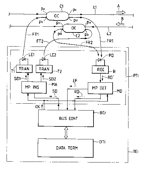
An embodiment of the present invention is
illustrated in Fi~. 3, in which the parts corresponding
~ 8 2043~96
to those in Fig. 1 are identified by the same reference
numerals and no description will not be given of them.
According to the present invention, a monitor pulse
appending circuit MA is provided between the bus
controller BCi and the transmitting circuits T1 and T2
of each terminal equipment TEi, the two lines of
photodetectors and receiving circuits in the prior art
are reduced to only one line, and a monitor pulse
detector MD is provided between the receiving circuit R
and the bus controller BCi.
In the motion pulse appending circuit MA, data
to be transmitted SD input thereinto is appended with
first and second 1/4 bit ling monitor pulses mpl and mp2
which rise up, for example, a 1/2 bit period and a bit
period, respectively, after the beginninB Of the low-level
period of the 3 bit long frame synchronizing signal SYN
of the data SD, as shown in Fig. 4. The resulting pieces
of data to be transmitted SD1 and SD2 are applied to the
transmitting circuits T1 and T2, respectively.
As in the prior art example, these pieces of data
SD1 and SD2 are modulated and converted into optical
signals, which are applied to the optical couplers C1
and C2. Optical signals branched from the optical
couplers C1 and C2 are applied via the optical fibers
FR1 and FR2 to a common photodetector PD, wherein they
are converted to electric signals, which are provided to
the common receiving circuit R. The received signal
RD' demodulated by the receiving circuit R has the
monitor pulses mp1 and mp2 in the low-level period of
the frame synchronizing signal SYN as shown in Fig. 4,
if the transmitting and receiving systems of the optical
couplers C1 and C2 and the optical transceiver PTi are
normal.
9 20~3~
In the monitor pulse detector MD it is checked
whether or not the monitor pulses mpl and mp2 are present
in each frame of the received signal RD' during
transmission from the terminal equipment TEi, and at the
same ~ime the monitor pulses mp1 and mp2 are removed
from the received signal RD', then the received signal
RD wi~h no monitor pulses as shown in FIg. 4 is applied
to the bus controller BCi. In the case where only one
or no monitor pulse is detected, some abnormality exists
in the signal paths for transmission and reception; so
that the error flag EF such as shown in Fig. 4 is
provided to the bus controller BCi.
The monitor pulse appending circuit MA has such
a construction as depicted in Fig. 5, for example. A
clock CK (32 MHz, for instance) and the date to be
transmitted SD shown in Fig. 6, supplied form the bus
controller BCi to input terminals 11 and 12, respectively,
are applied to a synchronizing bit detector 13 formed by
a counter. The synchronizing bit detector 13 counts the
number of clock pulses CK during the high-level period
of the transmission date SD and yields a detected siganl
S1 when the count value is equal to a value corresponding
to the 1.5 bit length. Accordingly, the detected signal
S1 is produced at the same time as the frame synchronizing
signal SYN goes low the 1.5 bit long period after its
rise to the high level (see Fig. 6) and the signal S1 is
applied to a monitor pulse generator 14. In the monitor
pulse generator 14 a timer is started by the detected
signal S1 and at time points 1/2 bit and 1 bit long
periods after the rise Or the detected signal S1,
respectively, the monitor pulses mpl and mp2 each of
the 1/4 bit length are generated in the low-level period
of the frame synchronizing signal SYN as shown in Fig. 6
~ 2043596
and they are provided to different output terminals 19
and 20. The first and second monitor pulses mp1 and mp2
thus derived at the output terminals 19 and 20 are
applied to OR gates 15 and 16, respectively, wherein
they are superimposed on the data SD, and the pieces of
data to be transmitted SDl and SD2 shown in Fig. 6 are
supplied to output terminals 17 and 18.
Fig. 7 illustrates an example of the construction
of the monitor pulse detector MD. The received signal
RD' applied from the receiving circuit R to an input
terminal 21, shown in Fig. 8. is provided to a synchro-
nizing bit detector 22 similar to that 13 in Fig. 5.
The synchronizing bit detector 22 generates a detected
signal S2 (see Fig. 8) at the same time as the frame
synchronizing signal SYN in the received signal RD' falls
the 1.5 bit long period after its rise to the high level,
the detected signal S2 being applied to a gate pulse
generator 23. In the gate pulse generator 23 a timer is
started by the detected signal S2 and a gate pulse GP of
a wid~h longer than thc 1 bi~ long~h bu~ shor~er ~h~n
the 1.5 bit length, as shown in Fig. 8, is generated in
the low-level period of the frame synchronizing signal
SYN. The gate pulse GP is applied to the one input
terminal of each of AND gates 24 and 25, which are
supplied at the other input terminals with the received
signal RD'. For only the duration of the gate pulse GP
the AND gate 24 is disabled, by which the monitor pulses
mpl and mp2 are removed from the received data RD', and
the received signal RD with no monitor pulses is provided
to an output terminal 26. In the AND gate 25 the gate
pulse GP and the received signal PD' are ANDed, by which
the monitor pulses mpl and mp2 are extracted as shown in
Fig. 8 and are applied to an error flag eenerator 27.
2043!~96
11
The error flag generator 27 checks the presence of the
monitor pulses mp1 and mp2 and, when one or both of them
are not detected, provides the error flag EF to an
output terminal 28. The clock CK is supplied from the
bus controller BCi to the synchronizing bit detector 22
via a terminal 29.
The foregoing embodiment of the present invention
has been described in connection with the case where a
frame synchronizing signal, which is not the Manchester
code, is detected and monitor pulses are inserted in the
received signal. The principle of the invention is
based on the face that the monitor pulses can be detected
in distinction from Manchester code data by detecting
the period durlng which the lo~ or hiBh logical level,
which is not the Manchester code data, lasts for the 1.5
bit length or more and then by inserting the monitor
pulses in a predetermined period subsequent to the
detected period. Accordingly, the present invention is
also applicable to the 4 bit long guard gap GG interposed
between the word strings each composed of a sequence of
frames. Thet is, in the guard gap GG which is the 4
bit long low-level period following each word string,
a predetermined period of time, for example, longer than
the 1.5 bit length, after the start of the low-level
period is detected and, as in the embodiment of Fig. 5,
the pulse S1 is generated. In consequence, the monitor
pulse generator generates the monitor pulses mpl and mp2
at two different time points after the above-noted
detected time point. In the arrangement in which the
synchronizing bit detector 13 detects a predetermined
high-level period (of the 1.5 bit length) and generates
the pulse S1, the predetermined low-level period can
be obtained simply by applying the date SD to the input
` 12 20~359~
terminal D of the detector 13 after inverting the logic
of the input data and by setting the clock CK counting
period in the detector 13 to the low-level period to
be detected. The synchronizing bit detector 22 of the
monitor pulse detector in Fig. 7 is constructed in the
same manner as mentioned above. The low-level period
can be distinguished from the low-level period of the
frame synchronizing signal SYN by selecting the former
to be longer than the latter. Thus, the two monitor
pulses need only to be produced the 1.5 bit length after
the start of the low-level period of the guard gap GG
but within 4 bit lengths.
It is evident that the principle of the present
invention is similarly applicable to the terminal gap
TG between sequence of word strings. In this instance,
the terminal gap TG can be distinguished from the low-
level period of the guard gap GG by generating two
monitor pulses until the end of the terminal gap TG after
the elapse of the low-level period longer than the guard
gap GG.
As described above, according to the present
invention, the two systems of photodetectors PD and
receiving circuits R needed in the prior art can be
reduced to one system by providing a simple-structured
monitor pulse appending circuit MA and a simple-structured
monitor pulse detector MD between the bus controller BCi
and the transmitting circuits T1 and T2 and between the
bus controller BCi and the receiving circuit R.
Furthermore, the comparator CP needed in the prior art
for checking the outputs of the two receiving circuits
with each other can be omitted. Thus, the present
invention permits economization and miniaturization of
the optical transceiver and also affords reduction of
~ 20435~6
13
the circuit scale, which provides for enhanced
reliability in the entire optical data communication
system.
According to the present invention, the trans- .-
mitted optical signals of each terminal, split by the
optical couplers C1 and C2, are applied via the optical
fibers FRl and FR2 to the common photodetector PD.
Accordingly, the output of the photodetecor PD has an
intensity twice higher than in the case where the
transmitted optical signals are individually received by
the two photodetectors PD1 and PD2 as in the prior art,
and hence the SN ratio is i~proved.
It will be apparent that many modifications and
variations may be effected ~ithout departing from the
scope of the novel concepts of the present invention.