Note: Descriptions are shown in the official language in which they were submitted.
CA 02044123 1999-12-23
./
t
1
STATIC SWITCH
BACKGROUND OF THE INVENTION
The invention relates to a static switch comprising a semi-
conductor, designed to be connected in series with a load to the
terminals of a DC voltage supply, and means for controlling an
operating voltage of the semi-conductor comprising means for
measuring the current flowing in the semi-conductor and means
for regulating the operating voltage of the semi-conductor in
terms of said current.
The French patent No 2,618,176 (Fran~ois), issued on
March 10, 1995, mentions in its introductiori a switch of
this type comprising means designed to make the switch
open when the current flowing through the latter exceeds a!
preset value for a certain time (circuit breaker function) and
limiting, by current regulation, the current in the semi-
conductor to a high value, lower than the current limits of the
semi-conductor, during the time delay period. To prevent
spurious trips, notably when the switch closes on a capacitive
load, the time delay must be sufficiently long. However, in the
event of a fault, the power dissipated in the semi-conductor is
high during the time delay, which makes limitation of this time
advisable. To reconcile these opposing constraints and enable
progressive switching limiting the overvoltages or overcurrents,
the above-mentioned document proposes a switching device,
designed notably for aeronautics, comprising semi-conductors
associated with resistors and connected in parallel so as to
form an electronic rheostat and which are turned on
successively, according to the current flowing through the
device.
SUMMARY OF THE INVENTION
The object of the present invention is to achieve a static
204412
2
switch, notably a power switch, which can be used without any
drawbacks with a capacitive load. Such a load is, for example,
constituted by the capacity of a cable, by a capacitor or by a
chopping power supply.
The switch according to the invention is characterized in that
the control means comprise a time delay circuit to one input of
which a switch closing or opening signal is applied, means
connected to an output of the time delay circuit, designed to
produce a rated operating voltage of the semi-conductor after a
preset time delay period following application of a closing
signal to the input of the time delay circuit, the regulated
operating voltage produced by the regulating means being applied
to the semi-conductor during said time delay period so that the
semi-conductor .operates, during this period, as a current
generator, limiting the current to a preset value much lower
than the rated current of the switch.
To give an example, the current can be limited to 100mA for 2s,
before switching to its rated value, for example 30A.
The switch preferably also comprises means of grounding the
semi-conductor operating electrode when a switch opening signal
is applied to the input of the time delay circuit and during a
very short preset time following application of a closing signal
in order to enable the regulating means to be zero reset.
According to a development of the invention, the means of
measuring the current are formed by a fuse connected in series
with the semi-conductor, the voltage at the terminals of said
fuse, representative of said current, being applied to the input
of the regulating means.
The use of a measuring shunt formed by a fuse or by an
equivalent resistance component enables the losses by thermal
204412
3
effect to be reduced to as great an extent as possible, when the
switch has its rated current flowing through it. In the case of
a fuse, the latter normally provides protection in the event of
the circuit breaker electronics failing. It can then act in
addition as a not very accurate shunt, at no extra cost. If the
regulated current, during the time delay period following
closing of the switch, is in the order of 100mA, the voltage at
terminals of the fuse is in the order of several hundred
microvolts. This very low DC voltage, applied to the input of
the regulating means, formed by an amplifying circuit and a
comparator, requires the use of an amplifier having a very low
offset voltage, and therefore relatively costly.
According to a development of the invention, the regulating
means comprise an amplifying circuit with automatic correction
of the offset voltage, which enables inexpensive operational
amplifiers to be used, whose offset voltage is much greater than
the voltage which is applied to their inputs.
An amplifying circuit of this kind preferably comprises a first
operational.~plifier whose output is connected to a first input
of a second operational amplifier and to a no-threshold diode
whose cathode is connected to a capacitor, the voltage at the
terminals of the capacitor being applied to the second input of
the second operational amplifier whose output constitutes the .
output of the amplifying circuit.
The switch can perform the function of a contactor, and/or of a
circuit breaker. When the switch operates as a contactor, the
closing and opening orders are external control signals. To
operate as a circuit breaker, a switch, preferably of the type
described above, comprises fault detection means producing an
opening signal in the event of an overload or short-circuit
being detected, and reset means producing a closing signal.
4
Conventionally the fault detection means comprise a fault
current measuring device, for example a shunt.
According to a development of the invention, the fault detection
means of the switch comprise means of detecting the voltage at
the terminals of the semi-conductor and means of producing the
opening signal when this voltage exceeds a first preset
threshold for a preset time, representative of an overload, or
when it exceeds a second preset threshold, representative of a
short-circuit, for which the semi-conductor is saturated.
Account is taken of the fact that the rated current flowing
through the switch is lower than the saturation current of the
latter and corresponds to a low preset voltage at the terminals
of the semi-conductor, whereas in the event of a short-circuit,
notably, the semi-conductor saturates and the voltage.: at its
terminals increases. Saturation of the semi-conductor in the
event of a short-circuit also enables the fault current in the
switch to be limited.
According to a particular embodiment, the collector of the
semi-conductor being connected to the DC voltage supply via the
load, the means of measuring the voltage at the terminals of the
semi-conductor comprise a diode whose cathode is connected to
the collector of the semi-conductor, and polarized so as to be
turned off when said collector voltage exceeds the second
threshold, the short-circuit detection means producing an
opening signal when said diode is turned off.
According to a preferred embodiment of the invention, the
semi-conductor is an insulated gate bipolar transistor (IGBT
type transistor), but the invention is also applicable to a
bipolar transistor or to a MOSFET type transistor.
BRIEF DESCRIPTION OF THE DRAWINGS
w~44~.2~
Other advantages and features will become more clearly apparent
from the following description of illustrative embodiments of
the invention, given as non-restrictive examples only and
represented in the accompanying drawings, in which
Figure 1 illustrates, in block diagram form, a switch according
to the invention.
Figure 2 represents the variation, in terms of time, of the
current in a switch according to the invention on closing.
Figure 3 illustrates certain details of an alternative
embodiment of a switch according to the invention.
Figure 4 is a representation of a particular embodiment of the
amplifying circuit of the switch according to figure 1.
Figure 5 represents the current/voltage characteristic of an
IGBT type transistor.
Figure 6 illustrates the fault detection principle in a static
switch.
Figure 7 represents a particular embodiment of a switch/circuit
breaker according to the invention.
DESCRIPTION OF THE PREFERRED EMBODIMENT
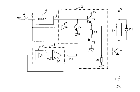
The static switch according to figure 1 is designed to be
connected in series with a load 1 to the terminals of a DC
voltage supply V1. In a conventional manner, a diode D1 is
connected in parallel on the load to limit the overvoltages at
the terminals of the latter. A switch of this kind is more
particularly a power switch designed to supply a load which may
6
be capacitive with a high voltage, for example 270V.
In the embodiment represented in figure 1, the switch comprises
an IGBT transistor T1 connected to the ground by means of a fuse
F. A supply voltage V2, for example in the order of 8V, supplies
the electronic components forming the control circuit of the
transistor 'T1.
The gate of the transistor T1 is connected to a control circuit
whose output stage 2 comprises a resistor R1 connecting the gate
to the ground and an npn-type transistor T2 whose base is
connected to an output 3 of a time delay circuit 4 and
connecting the gate to the supply voltage V2. A switch closing
or opening signal is applied to the input 5 of the time delay
circuit 4 by means of a switching circuit 6. The gate of the
transistor T1 is also connected to the ground by a grounding
circuit controlled by the input signal of the time delay circuit
4. The grounding circuit comprises, for example, a resistor R2
in series with a pnp-type transistor T3 whose base is connected
to the input 5 of the time delay circuit. A transistor T4, whose
base is connected by an inverter 7 to the input 5 of the time
delay circuit, connects the base of the transistor T2 to the
ground. The gate of the transistor T1 is in addition connected
by a resistor R3 to the output of a regulating circuit 8 to
whose input the voltage at the terminals of the fuse F is
applied.
The assembly described above operates as follows
When the switching circuit 6 is open, a low state logic signal
is available at the input 5 turning the transistor T3 on. This
logic signal, applied to the input of the inverter 7, also turns
the transistor T4 on, turning the transistor T2 off. The control
voltage applied to the gate of the transistor Tl is zero and the
transistor T1 is off.
7
When the switching circuit 6 is closed, a high state logic
signal is available at the input 5, turning the transistors T3
and T4 off. The signal available at the output 3 of the time
delay circuit 4, initially in low state, turning the transistor
T2 off, switches to high state after a preset time delay tl, for
example 2s, defined by the time delay circuit. After this time
delay tl, the transistor T2 is turned on and the supply voltage
V2 is applied to the gate of the transistor T1. This supply
voltage V2 corresponds to the rated control voltage of the
transistor T1 and a preset rated current, for example 30A, flows
through the transistor T1 to supply the load.
During the time delay tl, after a closing signal has been
applied to the control circuit of the switch, the transistors
T2, T3 and T4 are turned off and the gate voltage of the
transistor T1 is controlled by the regulating circuit 8 which
regulates the current in the switch to a reference value. The
fuse F acts as a measuring shunt, the voltage at its terminals
being proportional to the current flowing through the transistor
T1. This voltage is applied to the terminals of the regulating
circuit 8 comprising an amplifying circuit 9 whose output is
connected to an input (-) of a comparator 10. The other input
(+) of the comparator 10 is connected to a reference voltage
Vref, which can for example be derived from the supply voltage
V2 by a divider bridge or adjustable resistance. The transistor
T1 then operates as a current generator, the value of the
current being limited to a value, for example 100mA, much lower
than the rated current of the switch. The value of this inrush
current is fixed by the reference voltage Vref.
Figure 2 illustrates the variation against time of the current I
in the switch according to figure 1, when the latter closes. The
switch first operates as a current generator, producing a
constant current, of 100 mA, during the time delay period (2s),
~04~12
a
after which a much higher rated current, for example 30A, flows
through it. The time delay period is chosen so as to enable a
capacitive load 1 to be charged at a constant current up to the
DC voltage V1 before the end of the time delay, thus eliminating
any overload on startup due to the capacitive load being charged
too quickly.
Figure 3 represents in greater detail a particular embodiment of
the time delay circuit 4 and an alternative embodiment of the
output stage 2.
In this alternative embodiment, the pnp-type transistor T3 of
figure 1 is replaced by a MOS-type transistor T5, whose base is
connected to a second output 11 of the time delay circuit and to
the collector of a pnp-type transistor T6, whose emitter is
connected to the supply voltage V2 and whose base is connected
to the input 5 of the time delay circuit.
The time delay circuit is designed in such a way as to supply on
its second output 11 a complementary signal to the input signal
but delayed by a second preset time delay t2, much shorter
than the time delay tl mentioned above. To give an example, this
second time delay t2 may be in the order of one tenth of the
time delay tl.
With this alternative embodiment, an opening signal of the
switch (0 at input 5) turns, as previously, the transistor T4 on
and turns the transistor T2 off. At the same time it turns the
transistors T6 and T5 on, forcing the gate of transistor Tl to
zero. When a closing signal (1 at input 5) is applied at a time
to, the transistors T4 and T6 are turned off. The output 11,
initially at 1, remains at 1 for a time equal to the time delay
t2, T5 remaining on until the time to+t2 when it turns off. The
output 3, initially at 0, remains at 0 for a time equal to the
time delay tl, T2 remaining off until the time to+tl when it
G~4~~~
9
turns on. The closing cycle is thus divided into three periods
- A first period, between to and to+t2, when T2 being off and TS
on, the gate of transistor T1 is forced to 0.
- A second period, between to+t2 and to+tl, when T2 and T5 being
off, the gate voltage of transistor T1 is controlled by the
regulating circuit 8, transistor T1 operating as a current
generator.
- A third period, after the time to+t 1, when T5 is off and T2
on, making transistor T1 operate at its rated voltage.
The first period is designed to enable the amplifying circuit 9
of the regulating circuit 8 to be zero reset. In fact, during
this period, there is no current flowing through the fuse F and
the voltage applied to the input of the amplifying circuit is
zero.
Due to the use of the fuse F, of very low resistance, as current
measuring shunt, no high resistance is introduced into the
circuit. However the voltage at the terminals of the fuse is
very low, for example 200 microvolts for a current of 100 mA.
To enable such a voltage to be measured, the preferred
embodiment of the amplifying circuit 9, represented in figure 4,
comprises an automatic correction of the offset voltage.
This amplifying circuit comprises a first operational amplifier
OP1. The inverting input of the first amplifier OPl is connected
to the input of the circuit 9 by a resistor R4, and to the
output of the first amplifier by a resistor R5. Its non-
inverting input is connected to the common point of two
resistors R6 and R7 connected in series between the supply
voltage V2 and ground, so as to set the offset voltage Vo of the
amplifier OP1 to a preset value, for example +lOmV, higher than
the maximum offset voltage (+/- 7mV, for example) given by the
manufacturer.
w~~4~.~3
The output of the operational amplifier OP1 is connected to the
ground via a no-threshold diode 12 in series with a capacitor
C1. The voltage Vc at the terminals of the capacitor C1 is
applied to the non-inverting input of a second operational
amplifier OP2, whose inverting input is connected to the output
of the first operational amplifier OP1 by a resistor R8 and to
its own output by a resistor R9. The output of the second
amplifier OP2 constitutes the output of the amplifying circuit
9. In the figure, the no-threshold diode 12 is formed by a third
operational amplifier OP3 whose non-inverting input is connected
by a resistor R10 to the output of the first amplifier OPl, and
whose output is connected to the anode of a diode D2 whose
cathode is connected to the capacitor C1. The inverting input of
the amplifier OP3 is connected to the cathode of the diode D2.
The amplifying circuit 9 is thus formed by an inverting
amplifier (OPl, R4, R5) with a gain Kl=R5/R4, a no-threshold
diode 12, a capacitor C1 and a differentiating amplifier (OP2,
R8, R9) with a gain K2=R9/R8. To give an example, K1 can be
chosen equal to 100 and K2=10.
The amplifying circuit 9 operates as follows
The circuit input voltage being zero (switch open), the offset
voltage Vo of the first amplifier OP1 is multiplied by the gain
K1 of the latter and the capacitor C1 is charged at a voltage
Vc=Vo.Kl.
This value, corresponding to the amplified offset voltage, is
therefore stored in the capacitor C1.
When the switch closes a positive voltage Vf, corresponding to
the voltage at the terminals of the fuse F, is applied to the
input of the amplifying circuit 9. The~output voltage V3 of the
first amplifier is then given by
2~4~~~
11
V3 = (Vo - Vf).K1 (1)
This voltage is lower than the charging voltage Vc of the .
capacitor C1 and the no-threshold diode 12 prevents the latter
from discharging.
The differentiating amplifier (OP2, R8, R9) amplifies the
difference between the voltages Vc and V3 and supplies a voltage
V4 on output
V4 = (Vc - V3).K2 = Vf.Kl.K2 (2)
The voltage obtained at the output of the second amplifier OP2
corresponds to the amplified voltage Vf, the offset voltage of
OPl being corrected automatically. The offset voltage of OP2 is
for its part negligible compared with Vc-V3.
To give an example, for Vo=lOmV, Vf=100 microvolts, K1=100 and
K2=10, we obtain
Vc = 1V
V3 = 990mV
V4 = 100mV
A zero reset circuit, not represented, of the capacitor C1 can
be provided so that the stored offset voltage is correct when
the switch closes.
The switching circuit 6 of figure 1 can be controlled by
external control signals, the switch operating as a contactor.
The closing and opening signals applied to the time delay
circuit 4 can also be supplied by internal fault detection means
so as to bring about opening of the switch when an overload or
short-circuit is detected, reset means then being provided to
12
bring about closing of the switch which then operates as a
circuit breaker. Both types of function, contactor and circuit
breaker, can be combined without difficulty in the same switch.
Figures 5 and 6 illustrate the detection principle of a fault,
and more particularly of a short-circuit, in a static switch,
notably applicable to a switch as described above.
Unlike state-of-the-art fault detection circuits, the principle
described below does not use a measuring shunt designed to
measure the current flowing through the transistor T1. According
to the invention, the voltage Vce at the terminals of the
transistor T1 (figure 6) is used to detect a fault. For a preset
gate-emitter voltage Vge, for example equal to the supply
voltage V2, the current/voltage characteristic of the transistor
T1 is of the type, represented in figure 5. For a preset rated
operating current, for example 30A, the voltage Vce is in the
order of a few volts, for example 3V. In the event of an
overload, however, the current increases, at maximum up to the
saturation current, for example 150A, and the voltage increases
substantially, and can reach the level of the DC supply voltage
V1 of the switch.
Figure 7 represents a switch of the type represented in figure
1, comprising a particular embodiment of a short-circuit
detection circuit 13.
As the resistance of the fuse F is negligible, the collector
voltage of the transistor T1 is appreciably equal to the voltage
Vce of the transistor and is used to detect a fault. The cathode
of a diode D3 is connected to the collector of the transistor
T1. The anode of the diode is connected to the supply voltage V2
by means of a resistor R11. This resistor R11 is connected in
series, between V2 and the ground, with a Zener diode ZD and a
resistor R12. A transistor T7 has its base connected to the
c
lw S;~ ~:~ ~~ ~.~L ~ ea
13
common point of the Zener diode ZD and the resistor R12, its
emitter being grounded and its collector connected to the supply
voltage V2 via a resistor R13. The collector of the transistor
T7 constitutes the output of the detection circuit 13 and in the
event of a short-circuit supplies a tripping signal, or opening
signal, designed to be applied to the input 5 of the time delay
circuit ~. A reset pushbutton BP is connected in parallel to the
resistor R12.
In normal operation of the switch, the transistor T1 is on and
has flowing through it a rated current such that the voltage at
its terminals is in the order of 2 to 3V. The diode D3,
polarized by the resistor R11, is on. The Zener diode ZD has a
higher turn-on voltage than the voltage then present at the
anode of the diode D3 and is off. The transistor T7 is therefore
off and the output voltage of the detection circuit 13 is at its
high level. A closing signal of the switch remains applied to
the time delay circuit 4.
In the event of a short-circuit, the current I in the transistor
T1 becomes very great, while remaining limited to. its saturation
current, and the voltage on its collector increases. As soon as
this voltage exceeds the polarization voltage of the diode D3,
the latter turns off and the Zener diode, polarized by the
resistor R11 and the supply voltage V2 turns on, turning on the
transistor T7, whose collector switches to zero. The output
signal of the detection circuit 13, switching to zero, causes
the transistor T1 to turn off and the switch to open. The
collector voltage of T1 then remains high (V1) and the detection
circuit 13 continues to supply an opening signal (O) to the time
delay circuit.
The turn-on voltage of the Zener diode ZD, for example 6.2V, is
determined so as to supply a fault signal when the transistor T1
Y
14
is saturated. The fault current during a short-ci rcuit is then
limited to the saturation current corresponding to the voltage
applied to the gate of Tl.
To reset the switch/circuit breaker, the transistor T7 must be
off, causing the output signal of the fault detection circuit 13
to switch to 1. Reset means of this kind are represented
schematically in figure 7 by the pushbutton BP, closing of which
turns the transistor T7 off. The switch then closes in the
manner described with reference to figure 1 and, as soon as the
collector voltage of the transistor T1 is sufficiently low, the
diode D3 turns on again and keeps the transistor T7 turned off.
The switch/circuit breaker can be completed by a fault
indication circuit, by an overload detection circuit supplying
an opening signal in the event of detection of an overload, and
by an external control circuit enabling it to be made to operate
as a contactor as well. The overload detection circuit can also
use the variations of the transistor T1 collector voltage, the
transistor T1 collector~voltage exceeding a certain threshold
for a preset period being representative of an overload.