Note: Descriptions are shown in the official language in which they were submitted.
LOOKASIDE CACHE
The present invention r~lates to cache
architectures in computer ~ystems, and ~ore
~pecifically to a ~ kaside" ~licroprocessbr cache
architecture whereby 8 cache system is placed ~n the
processor' 6 local bus in parallel with the
~icr~pr~ce~sor and ~he memGry controller.
The computer industry is a ~ibrant and growing
field that continues to evolve as new innov~tions
occur. The driving force bshind this innovation has
~een the increasing demand ~or ~aster and ~ore powerful
computers. A ~ajor b~ttleneck in computQr speed has
historically been the ~peed with which data can be
accessed fro~ ~emory, referred to ~s the memory access
tim~. The ~icroprocessor, with its relatively ~ast
processor cycle times, has generally had to ~ait during
memory accesses to account for *he relatively slow
~Pmory ~ccess times. Therefore, impr~vement in memory
access times has been o~e ~ the ~ajor area~ o
research in enhanciny computer performance.
In order to bridge ~he gap between fast processor
~ycle ti~es and ~low memory access times, cache memory
was developed. A cache is a small amount of very fast,
~nd expensive, zero wait state memory t~at ls used to
store a copy of ~requently ~ccessed code ~nd data ~rom
system memory. The microprocessor can operate cut o~
this very fast ~emory ~nd thereby reduce ~he nu~ber of
.
- 2 ~
wait ~tates that must be interposed during memory
accesses.
The management or control of a ~ache iB generally
performed by a deYice referred to as e cache
controller. The cache contxoller i~ prineipally
responsible ~or keeping track Of the contents Of the
cache as well as controlling data ~ovement into ~nd out
of the cache. Another respons.ibility of ~he cache
controller is the pre~ervation of cache coherency,
which refers to the requlremen1: that the copy of ~ystem
~emory held in the cache be identical to the data held
in system ~emory. In additionl tha cache eontroller is
responsible for determining which memory ~ddresses are
capable of residing in the cache, referred to as
cacheable addresses. Certain ~egment~ of addressable
memory ~ay not be allowed to reside in the cache due to
cache csherency considerations. The cache controller
is therefore responsible for preventin~ data from non-
cacheable addre~sPs rom being placed in the caçhe.
Cache memory and its respective ca~he controller
are collectively referred to a~ a cache ~ystem. In
computer systems which inelude ~icroprocessor cache
systems, the cache ~ystem has generally been interfaced
in a serial fashion between the processor and the
system or memory bus. In this configuration, commonly
referr~d to as a "look-through" configuration, the
processor cannot talk directly ts the ~emory or ~ystem
bus, but rather the cache controller acts as the
primary ~ycle control interface between the memory or
system bus and the processor. When tbe processor
requires data and initiates a memory read, it pro~ides
the respective me~ory addresses and address and cycle
ontrol ~ignals to the cache contr~ller. The cache
controllar co~pares the~e addresses with the addresses
of the data re~sident in the cache.
2 ~
-- 3 --
Tf a cache read hit occurs, the cache controller
provides the requested data t~ the processor and the
control signals and ~ddress values are n~t passed on ~o
the ~emory or ~ystem bus. If the dat2 is determined to
be non-cacheable or ~ cache read miss occurs, then the
cache c~ntroller couples the addresses received from
the processor to ~he Demory or y~tem bus in the
computer ~ystem, ~nd the cache controller busses the
contr~l ~ignals to the ~y~tem or ~emory bus to perform
An operation on those buses. It is noted that there is
always a delay period, generally one cl~ck cycle,
bet~2en the processor providing the address values and
control signals an~ those values and ~ignals being
presented to the memory or ~ystem bus. When tbe data
is returned ~rom ~ys~em ~emory it is provided to the
processor ~nd is ~lso placed into the cache.
Write ~perations generally perfor~ differently.
In a write-through cache design all writes are passed
to the memory, but generally the operation is posted so
that the processor can proceed with no wait states. if
the write operations e~ceed the posting limit, then
operation is similar to a cache read ~i s. In a write-
bacX ~ache design, khe writes are performed only to the
cache, with the cache only providing the information to
the ~ystem when another p~rty requests the address.
The processor is released in zero wait ~tates in all
cases. Therefore, read operations are of primary
interest in removing delay periods from computer system
operation.
The addition of ~ microprocessor cache system to a
computer system g~nerally improves effective ~emory
access times considerably. However, the serial look-
through configuration described above whereby the cache
system is interfaced serially betwean the
microprocessor and the processor bus is ~ub-optimal
3 ~
~,
because on cache ~isses a delay is addled to the memory
~ccess ti~e that does not occur in computer ~y~tems
without microprocessor cache ~ystems. In computer
6ystems which do n~t include ~:icroprocessor c~che
~ystems, the processor initiates uemory read cycles
directly to the ~em~ry controller with~ut ~ny delay
interposed for a cache look-up~ This is in contrast to
what occurs on ~ cache ~iss in ~ look-through cache
configuration, whereby the cache controller must first
determine if the requested ~emory locations are cached
before initiating ~emory read cycles to th2 ~emory
controller. Therefore, a cache miss in a look-through
cache configuration interposes a delay between the time
that *he processor initiates the data request and the
time that ~ain memory read cycles are initiated on
cache ~isses, this delay being the time required for
the cache to dete~mine that the reguested data does not
reside there. As a result, the ~emory access time on a
cache miss in a computer ~ystem with a l~ok-through
microprocessor cache ~ystem is actually longer than the
~emory access time of a computer ~y~tem that does not
include a microprocessor cache system. The look-
through cache configuration reduces the efficiency of
~he cache ~ystem in this ~ituation by adding a delay to
the already 810w memory access ti~e ~n cach2 ~isses.
Therefore it is ~esirable that a cache system design
not impose any extra delays sn cache misses that would
not otherwise occur ig a ~icroprocessor cache system
were not included in the computer system.
The addition of a microprocessor cache system
increases the overall cost of the computer ~yst~m wh~le
at the ~ame time considerably reducing memory access
times in the computer ~ystem. Therefore, the addition
of a microprocessor cache ~ystem to a computer system
introduces a trade-off between increased cost ~nd
2 0 ~ rl
faster ~emory access ti~es. It i8 the!re~ore desirable
for a ~icroprocessor ~ache ~ystem ~e ~lade an ~ptional
and removable part ~f a computer ~ystem to ~llow a user
to tailor t~e computer 6ystem to fit ~rarious needs.
The present invention includes a lookaside
microprocessor cache design ~hlereby ~ cache syst~m is
6ituated on the processor's local bus ully in parallel
with tbe ~icroprocessor and the memory controller. In
~his ~anner, ~he ~emory ~ntro;Ller beginæ processor
~emory read cycles concurrentllr with the cache
~ontroller and thus no extra delay is ~dded to cache
misses. In addition, the lookaside cache design allows
the cache ~yste~ to be an optional and re~ovable part
of a per~onal computer ~ystem.
The cache controller and ~emory controller each
begin a processor memory read cycle simultaneously when
the processor initia~es a ~emory read. If the
processor cycle is a cache read hit, the cache
controller aborts the ~emory read cycle being perfor~ed
~y the memory controller and complates the processor
memory read cycle itself in zero wait 6tates. ~f he
processor cycle is a rache read ~iss, the ~emory
~5 controllar completes the ~emory read cycles as it
normally would if ths cache system were not present.
Since the cache controller ~nd the memory
controller both begin to service the processor re~uest
simultaneously, there is no added penalty ~or cache
misses. Furthermore, the lookaside architecture
permits the cache ~ystem to be optional since the
memory controller alway~ begins processor memory read
cycles and is aborted only on cache hits. ~hen the
cache 6yste~ is not installed, the memory controller
~5 interprets all processor cycles as cache ~isses.
- ' . ' : ~
,
:
,
2~4~87
Therefore, a user can tail~r hi6 personal computer
either for reduced cost by not i~cluding the cache
system or for faster memory access times by including
the cache ~ystem.
A better understanding of the invention can be
obtained when the following detailed description of the
preferred emb~diment is considered in conjunction with
the following drawings~ in which:
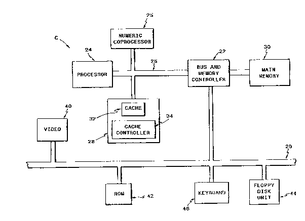
Figure 1 is a block diagram of a computer system
including a lookaside cache system according to the
present invention;
Figure 2 is a block diagram of the lookaside cache
system and its output siynal interface according to the
present invention;
Figure 3 is a more detailed block diagram of the
lookaside cache ~ystem and portions of its control
signal interface according to the present invention;
and
~ igure 4 is a flowchart depicting the
operation of the lookaside cache ~ystem during
processor memory read cycles according to the pr~sent
invention.
Referring now to Figure 1, a personal computer
system C is generally shown. Many of the details of a
computer system that are not relevant to the present
invention have been omitted for the purpose of clarity.
In the description that follows, a signal name followed
by an asterisk indicates that the ~ignal is asserted
when it has a low logic level and is the inverse of the
same signal name without an asterisk. ~he computer
syste~ C include.s a system bus 20 that is preferably
_ 7 _ 2~ 7
based on ~he Industry Standard AIcAit~cture ~ISA), a
bus architecture introduced in the International
Business Machines (IBM) ~T per~sonal computer.
c~ntroller rhip 22 comprising a bus controller ~nd a
memory controller is connected to ~he ~ystem bus 20.
Random ~ccess ~emory 30, hereinafter referred to as
main memory 30, is coupled to 1:he controller chip 22.
The controller chip 22 is coupled to a ~icroprocessor
24 ~hrough a local processor b-ls 26, which preferably
includes a processor address portion, a processor data
portion, and a control signal portion. The
microprocessor 24 i~ preferably an Intel Corporation
(Intel) 80386SX microprocessor according to the
preferred embodimeAt. Details on the operation of the
controller chip 22 beyond those ~iscussed in this
~pseification are considered known to those sXilled in
the art and are omitted for clarity.
~ lookaside cache system 28 ~ccording to the
present invention, which comprises cache ~emory 32 and
cache controller logic circuitry 34, is coupled to the
processor bus 26 between the processor 24 ~nd the
controller chip 22. A numeric coprocessor 25 may
optionally be connected to the processor bus 26. A
video ~ection 40 and read only memory (RON) 42 are
preferably attached to the system bus 20. Tbe ~ideo
section 40 preferably includes video memory, which
prefersbly includes video RAM and ROM. The main memory
30 and the ~ory loc~ted Dn the ~ystem bus 26 are
collectively referr~d to as system ~emory. A ~loppy
disk unit 44 and a keyboard 46 ~ay also be preferably
attached to the system bus 20.
The cache 32 accordi~g to the preferred embodiment
is preferably a 4 kbyte, 4-way 6et associative cache
with ~ line ~ize of 16 blts. ~he cache system 2B is
capable of caching the majority of logical ~emory
':' .. ' ' - ~
: . ~
. ~ ~ 4 ~ 3 7
-- 8 --
addres.ses compri~ing ~ystem memory~ Howeverl æome
~emory addresses are designated ~s non-cach~abl~
according to the preferr~d emb~diment. ~h~ cache
controller 34 according to the present. invention
includes logic circuitry which determines whether a
memory ~ddress gPnerated by the processor 24 i~
cacheable, ~r capable o~ residing in the cache 32. The
ca~he contr~ller 34 includes enabling ports and logic
circuitry which enable a user to enable or disable the
cache ~ystem 28 in th~ compute:r syste~ C.
Referring now to ~iyure 2, a ~ore detailed view of
the lookaside cache ~ystem 2~ depicting the ~utput
signals the cache ~ystem 28 uses to interface with the
processor 24 and the controller chip 22 is ~hown. The
cache controller 34 generates three control ~ignal
outputs, which are ~hown as ~eparate signal connections
apart from the processor bus 26 for clarity.
The cache controller 34 generates a cacheable
address signal referrad to as CA*, which is connected
to an input of ~he controller chip 22 referred to as
CA*. The cache controller 34 asserts th2 CA~ signal
low when the cache ~ystem 28 is enabled, the processor
~us cycle is a procassor ~emory read, and the addresses
generated by the processor are cacheable addr~sses.
Therefore, the cache controller 34 asserts the CA*
~iynal when a memory address generated by the processor
24 on a processor read cycle is acheable.
on a cache mi~s, the CA* signal acts as a reyuest
to th2 controller chip 22 that it return the data
requested by the processor 24 in 16 bit units, even lf
the processor only requested an 8 bit segment of data.
In this way, the cache controller 34 guarantees that it
will be able to allocate the data that is retrieved
~rom system memory and provided to the processor ~o
.that the data can be placed in the cache 32. I~ ~he
-
2 0 ~ 3 ~
g
~ddresses generated by the processor 24 reside in main
memory 30, the CA~ ~ignal informs the memory co~trGller
22 to return a ~omplete 16 bit data word fro~ ~ain
~e~ory 30, ev~n if the prDcessor 2~ or.ly requested an 8
S bit data word. If the regyest~ed ~emory ~ddress resides
in memo~y located on the ~yste~ bus 20 ~uch ~ in the
video ~emory or ~n the ROH 42, then the ~sserted CA*
sign~l directs the bus control:Ler 22 to return ~he
requested data in 16 bit units,. If the acoessed memory
located on the ~ystem bus 20 is 8 bit ~emory, ~he
asserted CA~ ~ignal directs the~ ~us controller 22 to
perform two 8 bit data bus cyc].es to return a full 16
bit word to the processor 24.
The cache controller 34 generates a read hit
~ignal referred to as RHIT*, which is connected to an
input referred to as AB~RT* on the controller chip 22.
The RHIT* ~ignal is asserted low by ths cache
controller 34 when a cache read hit occurs in the cache
32 on a process~r memory read cycle. The RHIT* signal
discontinues any further Dperation of the controller
chip 22 because the cache system 28 is able $o ~upply
the requested data to the processor 24. The asserted
RHIT* signal aborts the operation of the memory
controller if the data requested by the processor 24
resides in ~ain me~ory 24. If the requested data
resides in memory located off of the system bus 20, the
asserted ~HIT* ~ignal aborts the operation o~ the bus
controller. The RHIT* æignal is also asserted low by
the cache controller 34 when a processor reset signal
referred to as PRESET is active in order to indicate
the presence of the cache ~yste~ 28 to disagnostics
software. The RHIT* ~ignal is also asserted low during
I/0 read or write cycle~ to an internal registar inside
the cache cont:roller 34 in order to prevent the memory
controller from interpreting these read or write cycles
- lo ~ 7
as ~ystem bus ~ycles. The ~HIT* signa:L is otherwise
asserted BS a high value.
When the processor ~4 initiates a processor bus
cycle 6uch ~S ~ processor ~emory read, ~ne of ~ither
the cache controller 34 ~n the cache ~ystem 28, the
controller chip 22, or the numeric copr~ces~or 25 ~re
capable ~f responding. Therefore, the cache controller
34, the controller chip 22, and the numeric coprocessor
25 each generate a respective ready ~ignal referred to
1~ as the CRDY~ ~ignal, the MRDY* signal, ~nd the CPRDY*
~ignal, respectively. These ready signals are each
connected to an input of a 3 in;put AND gate S0. The
output of the AND gate 60 is connected to the ready
inputs (READY*) of each of the processor 24, the
numeric copr~cessor 25, and the cache controller 34.
Therefore, the assertion of one of the ready signals by
either the cache cDntroller 34, the controller chip 22,
or the coprocessor 25 informs the processor 24, the
coprocessor 25, and the cache controller 34 that the
processor bus cycla has been 6~rviced and thereby
terminates the processor bus cycle. The CRDY* signal
is asserted low by the cache controller 34 on cache
read hits in order to terminate processor bus read
cycles in zero wait states. The CRDY* signal is also
asserted when the processor 24 i6 programming an
internal register inside the cache contr~ller 34 in
order to terminate these cycles in zero wait states.
The CRDY* 6ingal is also asserted during processor
resets. Otherwise, the CRDY* ~ignal is a high value.
Referring now to Figure 3, a more detailed
~chematic diagram of portions of the control ~ignal
interface ~etween the processor 24, the numeric
coprocessor 25, the cache controller 34, and the
controller chip 22, i~ generally shown. This diagram
3S is intended to describe ~ome of the processor control
2 ~
~ignal6 utili~ed by the cache controller 34 during its
operation and is not intend~d to ke a comprehensive
analy~is of the co~plete control ~ignal interface
between ~he cache controller 34 and ~he variou~ other
components in the ~ystem C. The processor ~ddress bus
26 is ~own ~plit into a processor address portion 80
and a processor data portion 82, ~ach of which are
~hown 6haded or the purpose of cl~rity. The control
signal portion of the processor bus 26 is represented
by ~one of the respective contrDl signals generated by
the processor 24, which are shown individually for the
purpose of clarity.
The cache controller 34 and the controller chip 22
receive varisus control 6ignals generat~d by the
processor 24. For ~ore information on the ~arious
control signals generated by the microprocessor, please
refer to the 6pecification of the 80386SX
microprocessor in the 1989 Intel ~icroprocessor and
Peripherals Handbook, Volume 1, published by Intel,
which is hereby incorporated by reference.
The processor raset 6ignal PRESET is yenerat~d by
the controller chip 22 and is connected t~ the PRESET
inputs of the cache controller 34 and the process~r 24.
The PRESET signal is asserted high when a processor
rese~ is to occur, and this places the cache system 28
into a known reset stat~. The processor 24 generates a
data/control ignal referred to as the DC ~ignal, which
is connected to the DC inputs of the cache controller
34 and the controller chip 22. The DC ~ignal informs
the cache controller 34 and the controller chip 22 as
to whether the current bus cycle is a data cycle or a
code read or control cycle. The processor 24 generat~s
a memory/input-output 6ignal referred to as MIO that is
connected to the MIO inputs of the cache con~roller 34
and the controller chip 22. The ~I0 ~ignal ~nforms the
~Q~87
- 12 -
cache controller 34 and the controller chip 22 as to
whether the current processor bus cycle is directed to
the memory ~pace or the input/output (I/O) ~pace. The
processor 24 generates a wTitetread signal referred to
5 as WR that is connected to the WR input~ ~ the cache
controller 34 and the controller chip ~2. The WR
signal informs the cache controller 34 and the
controller chip 22 as to whether t:he current processor
bus cycle is a write cycle or a read cycle. The
processor 24 generates an address strobe signal
referred to as the ADS signal which is connected to the
ADS inputs of the cache controller 34 and the
controller chip 22. The processor 24 asserts the ADS
signal to indicate that a valid bus cycle definition
and address have been driven onto the processor bus 26.
The processor 24 generates two signals which enable
data onto the respective portions of the 16-bit data
bus. These ~ignals comprise a bus high enable ~ignal
referred to as the BHE signal and a bus low enable
signal referred to as the BLE signal. The BHF signal
and the BLE signal are connected to the BHE and BLE
inputs respectively of the cache controller 34 and the
controller chip 22. The BHE signal enables data onto
the most ~ignificant half of the 16-bit data bus, the
data bus lines D8 through Dl5, and the BLE ~ignal
enables data onto the least significant half of the lS-
bit data bus data bus, data lines D0 through D7.
~ eferring now to Figure 4, a flowchart
describing the operation of the cache system 28 during
a processor memory read is generally shown. It is
understood that nu~erous of these operations may occur
concurrently, but a flowchart format has been chosen to
simplify the explanation of the operation. The
processor 24 initiates a ~emory read in ~tep lOO and
provides the respective memory addresses to the
controller chip 22 by placing these a~dresses onto the
address portion of the local processor bus 26. The
controller chip 22 and the cache controller 34 receive
the memory sddresses generated by the processor 24 in
step 102. In step 104, the controller chip 22 beqins
~ervicing the remory reques If the requested data
resides in main memory 30, the memory controller begins
servicing the memory request. If the requested data
resides in a memory location physically located on the
system bus 20, such as either the video memory or the
ROM 42, the bus controller begins servicing the memory
request. Also, in step 104 the cache controller 34
checks the addresses generated by the processor 24 with
the addresses of the data resident in the cache 32 to
determine whether the requested data resides in the
cache 32.
If a cache hit occurs in the cach~ 32, the cache
controller 34 asserts the RHIT* signal to the
controller chip 22 in step lO~, which causes the
controller chip 22 to discontinue servicing the
processor memory read cycle. The cache controller 34
asserts the CA* signal in ~tep lO8, ~ignifying that the
addresses on the address portion of the processor
address bus 26 ~re ~acheable addresses. The cache
controller 34 also asserts the CRDY* signal to the
processor 24 in ~tep 108 in order to terminate the
memory read bus cycle initiated by the processor 24 in
step 100 in zero wait states. The cache controller 34
then provides the requested data to the processor 24 in
~tep llO, which is essentially contemporaneous with the
functions performed in ~tep 108.
3 ~
If a cache read mis~ occurs after the controller
chip 22 and the cache controller 34 begin ~ervicing the
memory request in 6tep 104, th~n the c~ntroller chip 22
continues servicing th2 ~emory request from the
pr~cessor 24 in steps 114 throtlgh 1~8. ~f th~ ~emory
~d~re~ses generated ~y the processor 24 ~re dee~ed to
be cacheable addresses ~y the c:ache controller 3~, then
the cache ~ontroller 34 asserts the CA* ~ignal t~ the
controller chip 22 in ~tep 114. As previously
discussed, the assertion of the CA* ~ignal directs the
c~ntroller chip 22 to return the requested data in 16
bit units. The controller chip 22 continues ~ervicing
the ~emory request in 6tep 114 and 116, this process
taking considerably longer than if the data were stored
in the cache 28 because of ~he slower ~e~ory access
time of ~ain ~emory 30 and ~emory located on the system
board 20. The controller chip 2~ provides the
requested data to the processor 24 in Btep 118. The
cache controller 34 allocates or latches the requested
data returned from the controller chip 22 in step 120
if it had previously asserted the CA* signal in step
114. As preYiously described, the assertion o~ the CA*
signal directs the controller chip 22 to return the
requested data in a 16 bit unita
When the processor 24 writ2s to system memory, the
cache controller 34 latches the respective ~emory
addresses generated ~y the processor 24 to determine if
these addre~ses reside in the cache 32. ~f the
generated addresses are cached, then the cache chip 2B
latches the respective data generated by the processor
24 in order to update the memory location in the cache
32. If the generated addresses are not cached, then
the cache ~hip 28 ignores the processor write t~yclesO
Therefore, processcr write cycles directly update
fl~7
- 15 -
Gystem memory ~nd also ~pdate the cache 32 if khe
addresses have ~lready b2en cached.
The cache system 28 ~ccorcling to the present
invention i~ an ~pti~nal part o~ the ~.omputer sy~t~m C
and is ~asily removable with ~i.nimal chang~s to the
system ~. In this ~anner~ th~ cache system 2~ behaves
like a coprocessor, ~nd the processor 24 i6 generally
oblivious as to whether or not the cache ~ystem 28 i6
present within the 6yste~ C. Referring again tD
Figures 2 and 3, when the cache system 28 is removed
~rom the computer syste~ C, the ABORT* and CA* input~
to the ~ontroller chip 22 ars at a logic high level due
to ~he effects of pull-up resistors 90 and 94, to
indicate that all processor memory read cycles are non-
cacheable and cache misses. The CRDY* input to the ~NDgate 60 is also tied to ~ logic high value, preferably
through a pull-up resistor 92, effectively ~aking the 3
input AND gate SO into a 2 input AND gate with inputs
CPRDY* and NRDY*. Thus, the lookaside cache system 2B
is easily re~ovable from the computer system C with
minimal changes to the computer ~ystem C.
Therefore, the present invention comprises a
lookaside cache design that allows a cache ~y~tem to be
an optional and removable part ~f the computer system.
In addition, the parallel lookaside design enables the
~emory controller or bus controller to begin processor
~emory read cycles concurrently with the ~ache systam,
thereby eliminatin~ any delay~ caused by cache ~isses.
The foregoing disclosure and description of the
invention ~re illustrative and explanatory thereof, and
various ch~nges in the ~ize, shape, materials,
components, circuit elements, wiring connections and
contacts, as well as in the details of the illustrated
circuitry snd construction may be made without
departing from the spirit o~ the invention.