Note: Descriptions are shown in the official language in which they were submitted.
2~4~
TRUE LEAST RECENTI.Y USED REPLACE~ENT
METHOD AND APPA RATUS
The invention relates to cache memory systems used
in computer systems, and more particularly to the
replacement of items when new items must be added to
the cache memory system.
Personal computers are becoming more powerful with
each passing moment, or 50 it seems. The performance
of the systems is great, but further performance is
always being demanded. To this end, ever faster
components are being used in the computer systems. The
development oP the key component of the computer
syst~m, the microprocessor, has outpaced the
development of memory devices designed to worX with the
microprocessor. The cycle times of the microprocessor
are quite low, 50 only very fast memory devices can ~e
used or the microprocessor sperations have to be slowed
down, thus decreasiny system performance. HoweYer, the
memory devices capable of operating at the required
speeds are relatively small and are expensiYe. Thus it
is generally cost prohibitiYe to construct th entire
main memory of the computer system using these fast
memory devices. Thus performance must suffer because
of economics.
One approach to resolve this conflict has been the
use of cache memory systems. In a cache memory systems
a small amount of ~he ~ast memory is used in
conjunction with a large amount of slower memory. ~he
slower memory ~orms the main system memory, while the
-- 2 --
small, fast memory contains portions o the data in the
slower main ~emory. The cache memory generally
contains recently used data, on the hope, which is
statistically based, that the data will be reused soon.
Then the data is available directly from tha fa5t cache
m~mory,.without the delay penalty develope~ when
accessing the slower main memory.
However, the cache memory is much smaller than the
main mem~ry and o some replac~ement policy is
necessary. Some data ~ust be removed from the cache to
allow new data to be stored. The most widely preferred
technique is the least recently used (LRU) technique.
In that approach the least recently used of a series of
locations is overwrit~en, thus keeping the newer data
available for use. While this is a desireable goal, in
practice it is quite ~ifficult to implement in certain
cases. Dep~nding on the number of ways in a set
associative cache d~sign the number of bits o~ memory
required to perform a true LRU is quite high.
Sufficient information must be kept to keep tracX of
the LRU way for each set in the cache. Additionally,
the total time ~o develop the LRU information must not
cause a delay in any cycle or either performance will
suffer or costs will increase.
To resolve some of these problems pseudo-LRU
techni~ues have been developed. One example of a
psuedo-LRU technique is the Intel Corporation i486
microprocessor, which uses a 4 way set associative
cache architecture. Three bits are provided to
determine first, which half of the ways was least
recently used and then second, which of the two ways in
the half was least recently used. This is a pseudo-
LRU technigue b~cause it does not account ~or properly
reshu~fling the order based on read hits to a
particular way. It is possible fox the least recently
2 ~ 8 ~
- 3 -
used way in a first hal~ to remain unused for a longer
period than both the ways in the ~econd half if the
most recently used way in the f irst hal f is continually
the basis of an intervening r~ad hit. Thus relatively
~tale data could be pre ent, clegrading cache system
performance.
` The major reason for employing pseudo-LRU
techniques is ~implicity of the logic and smaller
amount of memory rsquired for the LRU status
information. The designer must make a trade off
b2tween the per~ormance loss and the syst~m complexity,
and so many times pseudo-LRU techniques are used.
However, the pseudo-LRU techniques become much more
suboptimal as the total cache size gets smaller and khe
number of ways increases. Thus true LRU technigues
become more important or major performance losses can
occur.
The present invention allows the use of a true LRU
technigue without greatly complicating the logic or
using significantly greater amounts of memory for the
LRU status information. A four way set associative
cache is used, with six bits being used to store
indications of the LRU, LRU~l and MRU ways, with the
MRU-l way being determinable from those values. Th~
effect o~ intervening hit operations is fully
understood and compensations made. ~he operations work
in reverse order when snooping operations are
occurring, ~o that snooped locations are considered the
least recently used and the first replaced. A snoop
operation occurs when a bus master other than the
processor is accessing the memory and the cache
controller is monitoring the operation of the bus
master. Generally only bus master writes are of
2 ~ 8
concern because cache data maybe inva:Lid~ted in those
cases~
The six LRU bits for each 6et in the cache are
~tored in a random access memory (RAM) six bits in
width. During each memory operation the current values
are provided by the LRU RAM. If a processor operation
cache hit is occurring, that particular way is made the
NRU way, with an indication provided whether this way
was the LRU, the LRU~1 ~r the ~RU way. Using the
indications, the LRU values are shu~fled to indicate
the proper time reference a aging sequence of the ways.
If a processor cache read miss operation is occurring
the LRU way receives the data being read and is
designated as the MRU, with the remaining ways being
shuffled properly. If a snoop cache hit is occurring,
that particular way is made the LXU way, with an
indication whether the way was the LRU, LRU~l or MRU
way and the remaining ways being properly shu~fled.
The LRU information is o~tained and recalculated
each memory ~ycle but is written only when hits or
processor read cacha misses occur.
A ~etter understanding of the present invention
can be developed when the detailed description is read
in conjunction with the drawings, in which:
Figure 1 is a block diagram of a computer system
incorporating the present invention;
Figure 2 is a block diagram of the cache system of
the computer of Figure l;
Figure 3 is a timing diagram o~ various signals
used in the cache system of ~igure 2 and the c~mp~lter
of ~igure l; and
Figures 4 10 are schematic diagrams of portions
of the circuitry of the cache ~ystem of Figure 2.
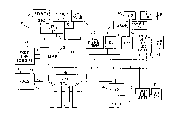
Ref erring now to Figure 1, a computer system
generally referrad to by the letter C is shown. The
computer 6ystem C includes a processor 20, preferably
an Intel C~rporation (Intel) 80386SX. Coupled to the
processor 20 are three buses r~eferred to as the PA, PD
and PC or processor ~ddress, processor data and
processor control buses, a numeric coprocessor 22,
preferably an Intel 80387SX and a cache ~ystem 24. The
cache system 24 incorporates the least recent used
(LRU) techniques of the present: invention. A series of
buffers 26 are used to couple the processor address bus
PA and processor data bus PD to the other various
portions of the computer C. For example, the buffers
26 an connected to a memory data bus MD, an external
bus including the external address bus XA and the
external data bus XD, and a system bus including the
system control bus SC, the system data bus SD and the
system address buses LA and SA. A memory and bus
controller 28 is connected to the processor address bus
PA and proce~sor control bus PC as well as the system
control bus SC and the system address buses LA and SA.
The memory and bus controller 28 is responsible for
converting the control ~ignals and addressing
information provided by the processor 20 to the signals
used in the cystem bus. Further, th~ memory and bus
controller 28 transfers ~ny control signals and
addrassing signals ~rom the various devices present
elsewhere in the system, generally another bus master,
to the processor buses PA and PC if appropriate~
Additionally, the memory and bus controller 28 provides
the memory control and addressing information to the
memory 30.
: " ' ' ,
2 ~ 8 ~
6 --
A direct memory access (DMA) 6y5t:em, an interrupt
controller ~nd various timers are included in a module
32 which is connected to the external address bus XA,
external data bus XD and the system control bus sC.
5 The read only memory ~ROM) 34 provided in the ~omputer
34 is also connected to the XA, XD and Sc buses. ~he
ROM 34 contains the basic operating instructions of the
computer ~ystem C. A keyboard controller 36, typically
an 8042 microcontroller, is also coupled to the XA, XD
and XC buses so that it is int~erfaced to the processor
20 for providing keyboard inputs received ~rom a
keyboard 38 cr mouse or other pointing device 40 to the
processor 20. A combined circuit ~2 provides the
parallel, ~erial and hard disk control ~unctions for
the computer C. Therefore a parallel port 44, a serial
port 46 and a hard disk unit 48 are connected to this
combined circuit 42. The combined circuit 42
communicates with the processor 20 over the XA, XD and
SC buses. Similarly, a floppy disk controller 50 is
also coupled ~ia the XA, XD and SC buses to allow a
floppy disk unit 52 to be controlled.
The video output of the computer C preferably
includes a VGA controller 54 which is coupled tv the
XA, LA, SA, SD and SC buses and to a monitor 56. A
series of slots 58 are also connected to the svstem
buses ~A, ~A, SD and SC to provide inclusion o~
interchangeable circuit boards if desired~ These
interchangeahle circuit boards can provide additional
~unctions or bus mastering devices utilized in the
computer C for individualization. It is noted that
when a bus ~aster is located in one of the slots 58 or
the DMA controller i8 operating, the processor 20 is in
a hold csndition and address and control information
and data provided by the bus master is provided through
the buffers 26 to the memory in bus controller 28 and
. 8 ~
- 7 -
reflected onto the processor ~uses PA, PD and Pc. ~hus
only one master device i5 operating at a gi~en time in
the computer system C.
The cache ~ystem 24 is shown in more detail in
Figure 2. The preferred embodiment of the cache system
24 is a.four way set associative cache having a total
si2e of 4K bytes. To this end the cache system 24
includes four banks of DA~A R~ lOOA, lOoB, lOOC ~nd
lOOD, which will be referred to generally as 100. Each
DATA RAM bank lOOA-lOOD is preferably 16 bits wide in
the preferred embodiment and includes separate input
and output data ports. Bits 9-1 of the processor
address bus PA are provided to the address inputs of
the DATA RAM 100. A signal referred to as DWE or data
~rite enable is provided to the DATA RAM 100 from a
timing and control logic module 102 as necessary when
data is to be written into the ~ATA RAM 100.
Additionally, signals referred to as DH and DL for data
hiqh byte and data low byte are provided by the timing
and control logic 102 to select which of the bytes of
the data word are to b~ provided or stored. Each bank,
which corresponds to a way of the cache system 24, of
the DATA RAM lOOA-lOOD i5 provided with an individual
chip select signal re~erred to as DRAMCS. ~he
2~ DRAMCS<3-0> ~ignals, for ways or banks 3 to 0, are
provided by the timing and control logic 102, thus
allowing independent operation of the particular ways.
The data outputs o~ the DATA RA~ 100 are provided to a
16 bit wide 4 to 1 multiplexer 104, whose routing is
controlled by ~ignals from the timing and control logic
102. The outputs of the multiplexer 104 are provided
to a 16 bit wide tristate buffer 106, whose outputs are
connected to the processor data bus PD. The output
control of the buffer 106 is provided by the timing and
control logic 102. The processor data bus PD is also
2 ~
connected to the inputs o~ a 16 bit wide buffer 108,
whose outputs are connected to the D or data inputs of
the DATA RAM loo.
In addition to data storage, the cache system 24
5 also includes a series ~f RAM's to contain the tags or
upper address values and line valid bits ass~ciated
with the particular data values stored at a location in
the DATA ~AM 100. The preferred tag value is the upper
14 bits of the address, with 2 bytes per line, 8 lines
per set and 64 sPts being valules of the cache
organization parameters. Because this is preferred to
be a four way ~et associative cache system, there are
four individual banks o~ TAG RAM's, generally referred
to as 110 and individually referred to as llOA, llOB,
llOC and llOD. The TAG RAM 110 is preferably 22 bits
wide to store the processor address bits 23-10 and
aight line ~alid bits referred to as LINE<7-0>. The
processor address bits PA<9-4> are provided to address
inputs of the TAG RAM 110 for addressing purposes. A
write enable signal referred to as is TAGWE provided by
the timing and control logic 102, while four signals
referred to as the TAGCS<3-0> are connected to the chip
select inputs of the TAG RAM's llOA-llOD. In this way
the timing and control logic 102 can detexmine when
data is written to the TAG R~M 110 and obtained from
the TAG RAM 110.
The outputs from the four TAG RAM's llOA-llOD are
provided to a comparator 112. Also provided to the
comparator 112 are the processor address lines 23-10
and 3-1 ~o that dete~minations can be made as to
whether the particular address being a~serted on the
processor address bus PA is pxesent in the cache system
24. Various control signals are ~lso received by the
comparator 112 from the timing and control logic 102.
~5 These 22 bits of data ~rom each bank of the TAG RAM's
g
- 9 -
llOA-llOD are proYided to the ~omparat~r 112, to be
used with the processor address ~igna:Ls 23-lo and 3-1
~or tag address and line valid checkiny.
The comparator 112 i5 also connected to a TAG
~ALID RAM 114. This RAM is preferably 4 bits wide, 1
bit corresponding to each way. The TAG VALID RAM 114
receives a~ address inputs the pr~cessor address lines
9-4 and provides 4 bits of data referred to as MOUT<3-
O> to the comparator 112. The comparator 112 provides
the ~IN<3-0> signals to the data inputs to the TAG
VA~ID RAMS 114. The comparator 112 therefore includes
the logic necessary to determi:n~ if a particular tag
value is present in the memory and whether the
particular line or tag value is valid. The TAG VALID
RAM 114 also receives ths TAGWE signal for write
enablement and the MRAMCS ~ignal for general RAM select
the timing control logic 102.
A 6 bit wide LRU RAM 116 is present in the cache
~ystem 24. The LRU RAM 116 is where the LRU data for
each set in the cache system 24 is stored. The LRU RAM
116 receives as address inputs ~he processor address
lines 9-4 and receives the TAGWE and LRAMCS signals
provided by the timing and con~rol logic 102 ~o the
write enable and chip select inputs. The 6 data
outputs, referred to as LOUT<5-0>, provided by the LRU
RAM 116 are sent to the LRU logic 118. The data inputs
to the LRU RAM 116, the LINc5-0> signals, are provided
by the LRU logic. Various signals ~re coupled between
the LRU l~gic 118 and the timing and control logic 107,
including the SNPCYCLE signal, which indicates that a
snoop cycle is in progress; the ALLOCATE* signal, which
is an indication that a cache read miss has occurred;
the MATCHc3-0~* signals, which are an indication that a
tag match has occurred; the LRUINIT signal which is an
indication th~t the LRU RAM 116 should be initialized
'
8~
-- 10 --
and the LRUWAY<3-0>~ signals, which indicate to the
timing and contr~ gic 102 which way ~hould be
~tilized to store data. A 6noop cycle is one where a
bus master, such as th~ DMA controller or a bus master
installed in a slot 58 has control of the ~ystem c and
is providing address information to the ~emory 30.
Snoop cycles are of interest, particularly write
cycles, because cache data can be invalidated if the
bus master writes to a memory :Location contained in the
cache. Thus the cache system 24 monitors snoop write
operations for possible line invalidation.
In review, the TAG RAM 110 contains the tag ~alues
and line valid values for each of the 128 sets in the
cache, while the TAG VALID RAM 114 contains values
indicating whether the tags for the sat are valid. The
LRU RAM 116 contains the LRU related information for
each set. The comparator 112 uses the tag values, the
line valid values and the tag valid values to determinP
if cache hits or misses occur for both processor and
snoop cycles and whether the mics is due to a line
being invalid or the entire tag being invalid. The LRU
RAM 116 and LRU logic 118 provide indications of which
way to use when new data must be stored in the cach~.
The timing of the various signals in this system
are shown in more detail in Figure 3. Four exemplary
cycles are shown, two read miss or allocate cycles, a
read hit cycle and a write hit cycle. T~e timing of a
snoop cycle is similar to that of an allocate cycle,
except that data is not written to the DATA RAM 100 and
the proper line bit is invalidated in the TAG RAM 110.
In the illustrated sequence the processor 20 has been
in an idle state and is commencing with a read
operation. The operation commences at time 200 where
the processor enters a Tl state. At time 200 the ~DS*
signal goes low to indicat~ that an address is bei~g
presented onto the bus. The address and control is
presented shortly after time 200. The CLX2 signal is
the basic timing signal used by the pr3cess~r 20 and is
present in the processor control bus PC. At time 202,
the next rising edge of the C~2 signal, the addr~ss is
c~nsidered ~ufficien ly ~table on the ~us and tag
comparison operation i5 commenced. To this end ~he
TAGEN or tag enable signal, the appropriate TRAMCS
signal, the ~RAMCS signal and the IRAMCS ~ignal are
driven high so that the tag ancl line values, the tag
valid information and the LRU i.nformation can be
obtained from the various ~AM'~. At time 204, the next
rising edge of the CLK2 signal, the TAGEN signal and
the TRAM, MRAM and LRAM chip select signals go low and
the ADS* signal goes high. The DATA RAM lO0 chip
select is activated in this case of a nonpipelined
operation to allow ~ero wait state operation.
Because the comparator 112 has d~termined that
this is a processor read cache miss or allocate
operation, new tay valu2 and line valid information
must be presented to the TAG RAM llO, new tag valid
information must be provided to the TAG ~ALID RAM 114
and the LRU values shuffled. Therefore at time 206,
the next falling edge of the CLK2 signal, the TAGWE
signal goes ~igh to prepare the various RAM's llO, 114
and 116 for a write operationO At time 2Q8, the next
rising edge of the CLR2 ~ignal, the appropriate TRAMCS
signal goes high, the HRAMCS signal goes high and the
LRAMCS signal g~es high. This causes the data which is
being pr~sented to the various RAM's to be stored to
update the tag valua, line valid bit, tag valid bit and
LRU data to reflect the new information which is being
~tored. A~ time 210, the next ~alling edge of the CLK2
~ignal, the DW:E or data write enable signal goes high
in preparation for wxiting data into the DATA RAN lO0
2~48g
- 12 -
because thi~ is a read mis~ and therefore the data
should be cached. At time 212, the next rising edge of
the CI~2 signal, ~he ADS* signal g~eg l~w to indica~e
$hat the next address is being presented onto the bus.
Also at this time the TA~ RAM 110, TAG VALID RAM 114
and LR~ RAM 116 chip select signals go low so that the
tag update is completed. At time 214, the next ~alling
edge of the CLK2 ~ignal, the TAGWE 6ignal is lowered to
complete the cache tag and LRu in~ormation write cycle.
At time 216, the next rising edge o~ the CLK2 signal,
the RDY* signal, which indicates that the first cycle,
cycle 1, has completed, is presented to indicate this
completion to the processor 20. Also at this time the
address 2 or second address has been fully presented
and it is appropriate to determine if there is a miss
or hit operation in progress. Therefore the TAGEN,
TRAM, MRAM and LRAN chip ~elect signals go high.
At time 218, the next rising edge o~ the CLK2
signal, the ADS* and RDY* signals go high. Also at
this time the tag related signals go low, the various
comparison operations having been completed. Finally
at this time, the DRAMCS signal that is appropriate for
the particular way goes high so that the writing of the
data into the DATA RAM 100 is performed. At time 220,
the next falling edge of the CLK2 signal, the TAGWE
signal goes high because it has been determined that
this is an allocate operation in the illustrated
embodiment and there~ore data must be written to $he
various RAM's t~ update the tag and LRU information.
At time 222, the next rising edge of the CLK2 signal,
the appropriate TRAMCS signal, the MRA~CS signal and
the LRANCS signals go high so that the new updated
information is written in~o th~ various RAM's, 110, 114
and 116. Also at this time the D~AMCS signal gOQS low
2 ~ 3 8
- 13 -
completing the write operation to the DATA RU~ 100 for
cycle 1.
At *ime 224, the next falling edge of the CLK2
signal, the DWE signal would go low if appropriate, but
in the illustrated case a ~econd allocate operation is
in progress and therefore the DWE signal stays at a
high state. At time 226, the next rising edge of the
CLK2 ~ignal, the ADS* signal goes low to indicate that
the address is being presented onto the bus for cycle
1o 3. At this time the update of the tag and LRU
information is completed and therefore the TRAMCS,
~RAMCS and LRAMCS signals go low. At time 228, the
next falling edge of the CLK2 signal, the TAGWE signal
goes low completing the tag information update
seguence. At time 230, the next rising edge of the
CL~2 signal, the RDY* signal goes low indicating the
completion of the second cycle. Additionally at this
time because the addresses are present and ~table on
the address bus, a tag check operation for the third
cycle ~ust be initiated. Therefore the TAGEN, TRAMCS,
MRAMCS and LRAMCS signals go high to allow the ~arious
information to be read. In the particular case of
cycle 3 this i~ a read hit operation, s~ tha~ the tag
data will not be updated, but only the LRU info~mation
needs to be updated. At time 232, tha next rising edge
of the CLK2 signal, the ADS* and RDY* signals go high,
indicating completion of the second cycle data phase.
~dditionally at this time the TAGEN, ~RAMCS, MRAMCS and
LRAMCS signals go low indicating that the tag checking
opera~ion has been completed. Finally at time 232 the
DRAMCS signal goes high ~or cycle 2 ~o that the data
present At ~he DATA R~M 100 is stored.
At time 234, the next ~alling edge of the CLR2
signal, the TAGWE signal goes high because thi~ has
been a read hit and it is necessary to update LRU RAM
!
,
2 ~ 3 ~
- 14 -
116. At time ~36, the next rising edge of the CLK~
signal, the LRAMCS signal is raised to enable the write
operation to occur to the LRU RAM 116. Also at this
tim~ the proper DRAMCS ~ignal or 6ignals are lowered so
5 that the write operation o~ the data of cycle 2 is
completed t~ the DATA RAM loO. At time 238, the next
falling edge of the CLR2 ~ignal, the DWE signal is
l~wered because it is no longe:r necessary to write data
to the DATA RAM 100. At time ;240, the nex~ rising edge
of the CLR2 signal, the ADS* s.ignal goes low indicating
that the addresses for the 4th cycle are b~ing
presented onto the address bus.. Additionally at this
time the IRAMCS ~ignal goes low to terminate the actual
write operation to the LRU RAM 116. ~inally at this
time the DRAMCS signal goes high while the DWE signal
is low, indicating that this is a read operation of the
DATA RAM 100 and thus the data is being provided from
the cache system 24 and not the main memory 20 for
cycle 3. At time 242, the next falling edge o~ the
CLX2 signal, the TAGWE signal goes low to complete the
cycle for writing to the LRU RAM 116. At time 244, the
next rising edge of the CLK2 signal, the ~DY* signal
goes low to indicate the completion of cycle 3.
Additionally at this time because the addresses are
present on the address bus for cycle 4, the TAGEN,
TRAMCS, ~RAMCS and LRANCS signals go high to obtain the
tag infsrmation. Finally at this time the DRAMCS
signal goes low to complete th read operation from the
DATA RAM 100.
At time 246, the next rising edge of the CLK2
signal, the ADS* and RDY* ~ignals go high indicating
that the data phase o~ the third cycle is completing.
Additionally at this time the various tag related
signals go low ~o indicate that the tag read and
comparison operation has been completed. At time 248,
3 ~
- 15 -
the next ~alling edge of the CLK2 signal, th~ TAGWE
signal g~es high ~ecause this has bee;n determined to be
a write hit and there~ore, while ~he TAG RAM 110 need
not be updated, the LRU RAM 116 must be updated and
therefore the TAGWE signal must be raised. At time
250, the next rising ~dge of t:he CLK2 signal, the
LRAMCS signal is raised to write the new LRU
information into the LRU RAM 116. At time 252, the
next falling edge of the CLK2 signal, the DWE signal is
raised because this is a write! hit operation and
therefore data ~ust be provided to the DATA RAM lO0.
At time 254, the next rising edge of the CLK2 signal,
the LRAMCS signal is lowered to complete the writing of
the LRU information to the LRU RAM 116. At time 256,
the next falling edge of the CLK2 signal, the TAGWE
signal is lowered. At time 253, the next rising edge
of the CLK2 signal, the RDY* signal is lowered to
indicate the completion of the data phase of cycle 4.
It is noted that a new ~DS* signal has not been
provided because the processor 20 is entering an idle
state and ther~fore no address need be presented. At
time 260, the next rising edge of the CLK2 signal, the
RDY~ signal is raised and the DR~MCS signal is raised.
Thus the data is written into the DATA RAM lO0, the
operation ~ing cQmpleted at time 262, the next rising
edge of the C~K2 signal, when the DRANCS signal is
lowered~ To complete the cycle the DWE signal is
lowered at time 264, the next falling edge of the CLK2
signal.
Therefore it can be seen that for each memory
operation the TAG RAM 110, the TAG VALID RAM 114 and
the LRU RAM 116 are read, while the TAG RAM 110 and the
TAG VALID RAM 114 are written only i~ in~ormation needs
to be updat2d, such as new addresses during allocation
cycles or invalid bits during snooping ~ycles, and the
.
- ' :
2~fi~
- 16
LRU RAM 11~ is written each time a hit or allocate
cycle occurs to keep the LRU information current.
Proceeding now to some of the more detailed
schematics of the LRU logic 118 and the ti~ing and
control logic 102, the 6 bits of information provided
by the LRU RAM 116 are received at the inputs oP 6
inverters 300. It i5 n~ted that bit~ 0 and 1 of the
LRU RAM 116 contain information related to which was
the least recently used way of the four ways in the
set, while ~its 2 and 3 indicate the LRU~1 way or next
to least recently used and bits 4 and 5 indicate the
most recently used (MRU) way. It is noted that 2 bits
are associated with aach way because with four ways in
the cach~, two bits are necessary to indicate each way.
Only three sets need be saved because the fourth way,
the ~RU-l way, can be developed from the other three as
will be shown. The outputs of the inYerters 300 are,
respectively, the BLOUT~5-0>* signals.
The BLOUT<0>* signal is provided as one input to a
two to one ~ultiplexer 302. The BLOUT~1>* signal is
provided to a similar input of a second two to one
multiplexer 304. The other input to the multiplexer
302 is provided by the output of a two input NAND gate
306. One input to the NAND gate 306 is the MATCH<1>*
signal which, when lo~, indicates that a match has been
made on way 1~ A second input to the NAND gate 306 is
the MATCH<3>* signal, ~hich, when low, indicates that a
match has been made with way 3. The second input to
the multiplexer 304 is provided by the output of a two
input N~D gate 308, one of whose input signals is the
MATCH<3>* signal. The other input to the NAND gate 308
is the ~ATCH<2~* signal, which when low, indicates that
a mat~h has been made to way 2 of the cache. A match
~or purposes of t~is ~pecification is when the tag
~5 address values match the presented address, the various
.
' ,.,'', '. ' ,..'
.. .
. .
. . .
2~l~4.~$
- 17 -
valid bits being ignored in dPveloping the MATCH*
signals. The ~elect inputs t~ the multiplexer 302 and
304 are provided by the output of an inverter 310 whose
input is the ALLOCATE* signal. The Al,LOCATE* 6ignal is
low when a cachPable allocate or proc~ss~r read miss
operation is occurring. The output of the multiplexer
302 is the LRUMUX<0~ signal, while the output of the
multiplexer 304 is the LRUMUX<1> signal. The LRUMUX
signals indicate the way that ~will be selected from the
DATA RAM 10~ either based on a match which is developed
as a result of a hit, either a processor based read or
write hit or a snoop hit, or t11P least recently used
way in the case of an allocate cycle.
The LRUMUX<0> signal is provided as one input to a
2 input AND gate 312. The other input to the AND gate
312 is provided by LRUINIT* signal which, when l~w, is
an indication that the LRU RAM 11~ is being
initialized. Similarly, the LRUNVXcl> signal is
provided as one input to a 2 input AND gate 314, the
other input being the LRUINT* signal. The outputs of
the AND gates 312 and 314 are the ACCESS~1-0> signals,
which represent the way being accessed from in hit
oper~tion or to be aceessed in read miss operations in
th~ particular memory operation.
The LRUMUX<0> and LRUMUX<l> signals are also used
as inputs to a series of EQUAL gates to determine if
the LRU, LRU+l or MRU way is currently being accessed.
The LRUMUX<0> signal is provided as one input to EQUAL
gates 316, 31~ and 320, while the LRUMUX~1> signal is
provided as ~ne input to a series of 2 input EQU~L
gates 322, 324 and 326. The second input to the EQUAL
gate 316 is the BLOUTc0>* signal, while the second
input to th~ EQUAL gate 322 is the BLOUTcl~* signal.
The outputs of the EQUAL gates 316 and 322 are khe tWD
inputs to a 2 input NAND gate 328, whose output is the
:
2 ~ 8
- 18 -
L~U EQ ACCESS* signal. Therefore if the way currently
being or to be accessed is ~he LRU way, th~
LRU_EQ_ACCESS* 6ignal goes low.
The sec~nd input to the EQUAL gate 31B is the
BLOUT<2>* signal, while the second input to th~ ~QUAL
gate 32~ is the BLOUT<3>~ signal. Th~ outputs o~ the
EQUAL gates 318 and 324 are prDvided to the two inputs
of a 2 input NAND gate 330, wh3se output is the
LRU+l EQ_ACCESS* ~i~nal. Similarly, the BL~UT<4>*
lo ~ignal is provid~d ~s the second input to the EQUAL
gate 320 while the BLOUT<5>* s:ignal is pro~ided as the
~econd input to the EQUAL gate 326. The outputs of the
EQUAL gates 320 and 326 are the inputs to a 2 input
NAND gate 332, whose output is referred to as the
MRU EQ_ACCESS* signal. Therefore the EQUAL yate sets
are usPd to determine if one of the stored w~ys is
being accessed.
It is further nec~ssary to determine the MRU-l way
and this is performed by two 3 input XOR gates 334 and
336. The three input XOR gate 334 receives the
BLOUTcl>*, BLOUT<3~* and BLOUT~5>* signals, while the 3
input XOR gate 336 rec2ives the BLOUT<O>*, BLOUT<2>*
and BLOUTc4>* signals. The output of the XOR gate 334
is the MRU~ * signal, while the output of the XOR
gate 336 is the MRU-l<O>* signal. Thus it can be seen
it is necessary to ~tore only 3 of the 4 ways and that
the fourth way can be devaloped readily. Because each
hit or allocate cycle causes data to be read or
written, it is necessary to update or shuffle the LRU
values on each of those operati~ns. The following
equations are used tv determine the way shuffling
occurs in the LRU RAM ~16. If a processor cycle is
occurring, the equations are as follows:
MRU = ACCESS
L2U+l - M~U~ (ACCESS = LRU) ~ (ACCESS = LRU+l~
I L~
-- 19 --
~ LRU+l if (ACCESS e 2~RU) + (ACCESS = MRU-l)
LRU = LRU+l if (ACCESS ~ LRU)
~ LRU if (ACCESS `~> I~.U)
wher~ ACCESS is the value o~ the way ~urrently being or
to be accessed.
Thus, the way being or to be accessed i5 Bet as
the ~RU way, while the LR~ way remains the previous LRU
way if the LRU way is not being or to be accessed or
is assigned the previous LRU+l way if the LRU way is
being or t9 be accessed. The ~IRU+l way stays the
previous LRU+1 way if tbe ~RU or MRU-1 ways are being
or to be accessed or is set to the previous MRU-1 way
if the LRU or LRU+l ways are being or to be accessed.
If a SnOGp cycle is occurring the following
equations are used:
MRU = MRU if (ACCESS c> NRU)
~ MRU-1 if (ACCESS = MRU)
LRU+l = LRU+l if (ACCESS = LRU)
+ LRU if (ACCESS <> LRU)
LRU = ACCESS
Thus the way being or to be accessed is set to be
the LRU way. This differs from the processor-based
case because this location is now invalid because of
the snoop hit and thus the chance of valid data not
being replaced is increased. The ~RU way stays the
previous MRU way if the access is not to the ~RU way or
is set tô the previous MRU-l way if the access is to be
MRU wayO The LRU~l way stays the previous LRU+l way if
the access is to the previous LRU way or is set t~ the
previous LRU way if the access is not to the previous
LRU way.
Thus ~he shuffling or reshuffling is properly
based on time ~ince pr~cessor access, the use age of
the way.
8 ~
- 20 -
This shuffling is developed using a series of
multiplexers as shown in Fig. 5. The LINcl-0> signals,
which are two of the inputs to the LRU RAM 116, are
provided by the inverted outputs of a 2 bit wide 2 to 1
multiplexer 350. The ~election input to the
multiplexer 350 is provided by the output of an
inverter 352 which receives at its input the LRUINIT*
signal. The B inputs to the multiplexer 350 receiv~
two high values so that if the LRU RAM 116 is to be
initiali~ed, as indicated by the LRUINIT* signal being
low, the LIN<1-0> signals are both low, indicating that
way O was least recently used. The second set of
inputs to the multiplexer 350 is provided by the
outputs of a two bit wide 4 to 1 multiplexer 354. The
B selection input to the multiplexer 354 is provided by
the SNPCYCLE signal, while the A or lower order bit of
the multiplexer selection is provided by the output of
a two input AND gate ~56. One input to the ~ND gate
~56 is the SNPCYCLE* or inverted SNPCYCLE signal, while
the other input is th2 LRU EQ ACCESS* signal. The
BLOUT<3-2>* signal~ are provided to the 00 inputs of
the multiplexer 354, while the BLOUT<1-0>* signals are
providad to the 01 inputs of the multiplexer 354. The
ACCESS<l-O> signals are provided to the 10 inputs,
while low values are provided to the 11 inputs.
Therefore, if a snoop cycle is occurring, the 10 input
is selected at the multiplexer 354. Thus the accessed
way in a snoop cycle is always indicated as the least
recently used way. If a snoop cycle is not occurring,
then the selection is between inputs 00 and 01,
depending upon whether the way being accessed was the
previously least racently used. ~f so, then the
BLOU~<3-2~* signals or LRU+l value is provided to the
LRU. If not, then the one input is selected and the
current LRU value is passed through and remains the LRU
~alue.
A 2 bit wide 2 to 1 multiplexer 358 is utilized to
provid~ the LIN<3-2> ~r LRu~l info~mation to the ~RU
RAM 116. The LIN<3-2> ~ignal is provided by the
inverted outputs of the ~ultiplexer 358, whose select
input is provided by the output of the inverter 352.
The B or ~econd channel inputs to the multiplexer 358
are provided by high and low s:ignals, respectively, so
that upon initiation of the LRU, the LRU+1 indication
is way 1. The second inputs oi. the multiplexer 358 are
provided by the output o~ a 2 bit wide 4 to 1
multiplexer 360. The 00 inputs to the multiplexer 360
are provided by the BLOUT<3-2>~ signals, while the 01
inputs are provid~d by the MRU-1<1-0>* signals. The 10
inputs to the multiplexer 360 are provided by the
BLOUT<1-0>* signals, while the 11 inputs are connected
to low level sig~als. The least significant bit of the
selection inputs in tAe multiplexer 360 is provided by
the output of a two input ~ND gate 362. An inverted
input to the AND gate 362 is connected to the SNPCYCLE
signal, while the other input to the AND gate 362 is
provided by the output of a two input NAND gate 364.
One input to the NAND gate 364 is the LRU EQ ACCESS*
signal, ~hile the other input is the LRU+l_EQ ACCESS*
signal. The high order bit o~ the selection inputs of
the multiplexer 360 is provided by the output of a two
input AND gata 366. One input to the AND gate 3~6 is
the SNPCYCLE, signal while the other input is the
LRU EQ ACCESS* signal. This connection of the
multiplexers 360 and 358 with the associated logic
circuitry 362, 364 and 366 provides the LRU~l equations
as indicated above for the snoop and processor cycles.
The MRU or LIN~5-4~ bits are provided at the
invert~d outputs of a two bit wid~ 2 to 1 multiplexer
- 2~ -
368. The ~election input to the multiplex~r 3s8 is
provided by the output of the inverter 352~ while the B
or ~econd channel inputs are connected to two low
inputs so that upon initiation of the LRU RAM 116 the
~ost recently used way is considered to be way 3. The
s~cond set of inputs to the ~ultiplexer 3~8 is provided
by the outputs of a two bit 4 to 1 multiplexer 370.
The 00 inputs to the multiplex~er 370 are provided by
the BLOUT<5 4>* signals, while the 01 inpu~s receive
the MRU-l<l-O>* signals. The :LO inputs receive the
ACCESS<l-O> signals, while the 11 inputs have both bits
connected to a low level signa]L. The least significant
selection bit of the ~ultiplexer 370 is provided by the
output of a two input NOR gate 372. One input to the
NOR gate 372 is provided by the MRU_EQ ACCESS* signal,
while the other input receives the SNPCYCLE* signal.
The high order selection bit of the multiplexer 370 is
connected to the SNPCYCLE* ~ignal. There~ore it can be
seen that this combination of the multiplexers 368 and
370 and gate 372 provides the functionality of the
equations for the MRU as indicated above.
It is noted ~hat this LRU reshuffling logic is
activ~ at all times for sach access and therefore chip
selection and write control logic is n0cessary to
properly sava the LRU reshuffling information only on
processor read or write hit operations, snoop hit
operations and allocation or processor read miss
operations. This logic is detailed in the following
figures.
One of the functions of the LRU logic 118 is to
provide to the timing and c~ntrol logic 102 an
indication into wnich way data is to placed in an
allocate situation. This logic i6 shown in Fig. 6. A
two input AND gate 400 receives as its inputs the
BLOUT~1>~ and LRUINIT* signals. A second two input ~ND
gate ~02 receives as its inputs the BLOUT~0>~ and
LRUINIT* ~ignals. An inverter 404 is connected to the
~utput of the AND yate 400, while an inverter 406 is
ronnected t~ ~he ~utput of the AND gate 402. The
desired LRU way indications are provided by the outputs
of 4 two input NAND gates 40~, 410, 412 and 414. The
two inputs to the NAND yate 408 are the output o~ the
AND gate 400 and the output Df the AND gate 402, with
the output of the NAND gate 4013 being the LRUWAY<3>*
signal, which indicates that way 3 is to be utilized.
The inputs to the NAND gate 410 are provided by the
output of the AND gate 400 and the output of the
inverter 406 so that the output o the NAND gate 410 is
the LRUWAY<2~* ~ignal, to indicate that way 2 is to be
selected. The inputs to the NAND gate 412 are the
output of the AND gate 402 and the output of the
inverter 404, so that the output of the NAND gate 412
represents the L~UWAY<1>* signal to indicate that way 1
i~ to be u~ed. The LRU~AY<0>* signal is produced as
the output o~ the NAND gate 414, which receives as
inputs the outputs of the inverters 404 and 406. Thus
for allocate operations the least recently used way is
directly indicated and decoded for use by the timing
and control logic 102.
The TAGWE signal is produced as shown in Fig. ~.
The BA~S signal, a buffered and inverted version o~ the
ADS* signal provided on the processor control bus ~C,
is provided as one input to a two input NAND gate 420.
The TAGEN signal, indicating that a tag access lookup
cycle is in progress, is provided ~s a second input to
the NAND gate 420. The output of the NAND gate 420 is
one input to a four input NAND gate 422. A second
input to the NA~D gate 422 is th2 T2P~ signal, which
indicates that the processor 20 or processor bus is not
35 in state T2P. This state condition can be shown on the
~V~4~
- 24 -
timing diagram of Fig. 3~ where the pro~essor bus
states are shown. A third input to t~e MAND gate 422
is the SNPWE* signal, which indicates that ~ write
operation is in progrsss ~nd a bus ~aster i5 in
control. The final input to the NAND gate 422 is
provided by the output of a two input N~ND gate 424.
One input to the NAND gate 424 is the SYNCTAG sig~al,
which when active high indicates that the bus cycle is
in a state where a tag and LRU value update or write
~hould occur, if necessary. The sPcond input to the
NAND gate 424 is the noninverted output of a D-type
flip-flop 426. The D input to the flip-flop 426 is
provided by the output of the NAND gate 422, while the
clocking signal to the flip-flop 426 is provided by the
CLR2 signal. The noninverted output to the flip-flop
426 is also provided to the D input of a latch 428.
The inverted enable input of the latch 428 is connected
to the CLK2 signal, with the inverted output is
connected to an inverter 430. The output of the
inverter 430 is the TAGWE signal. Thus the TAGWE
signal is produced as shown in Fig. 3.
A state machine is provided to det~rmine where
operation is in a snoop cycle. This state machine i~
shown in Fig. 8. The Tl* signal, which indioates when
low that the proces~or 20 bus is in state Tl; the
HOLDA* signal, which indicat~s when low that th~
processor 20 is in hold; and ~he SNPSTB* signal or
snoop strobe signal, which is true low when a snoop
write operation is occurring, are presented as the
inputs to a three input NOR gate 440. Th~ outpu~ of
the NOR gate 440 is provided to the D input of a D-
type ~lip-~lop 442. The clocking input to the flip-
~lop 442 is provided by the CLK2 signal. Th~ non-
inverted output of the fli~-~lop 442 is provided to the
D input o~ a D-type flip-flop 444, whose clocking input
25 ~
is also provid~d by the CLK2 signal. The noninverted
output of the flip-fl~p 444 is the SNOOPING signal,
while the inverted output is the SNPCYCLE* ~i~nal,
which indicates that a ~noop cycle is in progress when
low. The SNPCYCLE* signal is provided to inverting
inputs ~f two AND gates 446 and 448. The second input
to tAe AND gate 446 is provided by the output of a two
input NAND gate 450. One of the inputs to the NAND
gate 450 is provided by the inverted output of a D-
type flip-flop 452, while the other input to the NAND
gate 450 is provided by the inverted output of a D-
type 1ip-flop 454. Both of the flip-flops 452 and 454
are clocked by the CLK2 ~ignal. The output of the AND
gate 446 is provided to the D input of the flip-flop
452 and to an inverter 456. The output of the inverter
456 is the SNPWE* ~ignal. The noninverted output of
the flip-flop 452 is the SNPB signal, while the
inverted output is the SNPB* signal. The SNPB* signal
is provided as one input to a two input NAND gate 458.
The second input to the NAND gate 458 is provided by
the noninverted output of the ~lip-flop 454. The
output of the NAND gate 458 is connected to the second
input of the AND gate 448. The D input o~ the flip-
flop 454 is ~onnected to the output of the NAND gate
448. Thus ~ ~tate machine is developed to track the
cycling of a snooping operation.
The SNPA* signal, the inverted output of the flip-
flop 454, and the SNOOPING signal are provided as two
inputs o~ two three input N~ND gates 460 and 462. The
third input to the NAND gate 460 is the SNPB* signal,
whil~ the third input to ths NAND gate 462 is the SNPB
signal. The output of the NAND gate 460 is the
SNPCHECX* signal, which indicates the time in a snoop
bus cycle to perform a tag read operation, while the
output of the NAND gate 462 is provided as one input to
- 26
a two input OR gate 464. ~he other input to the AND
gate 464 is the IHIT* ~ignal, which will be defined
later, with the output of the OR gate 464 beiny the
SNPLRU* signal, whose use will also be indicated later.
Portions of the circuitry forming the comparator
112 are.shown in Fig. 9. The .illustrated circuitry
determines if matches and hits have been developed.
Shown in Fig. 9 is the circuitry for one way ~f the
comparator 112, but it is note~ that four similar
grvups of circuits are provided in ~he compa~at~r 112
to perform the comparison operations for e~ch ~ th2
four ways. The difference between the group~ is
indicated by the small n sy~bol in the Figure. The
stored tag address output values or TOUTn<23-10> from
the TAG RAM 110 are provided to a ~eries of 14 EQUAL
gates 470. The second inputs to the EQUAL gates 470
are ~he processor address bus PA bits 23-10, so that
this ~eries of EQUAL gates 470 performs the lookups and
matching to determine if the tag address ~alues are
equal to the presented address values. The 14 outputs
of the EQUAL gates 470 are provided to a series of AND
gates 472, 474, 476 and 478. The AND gates are all
four input AND gates with all of the inputs to AND
gates 472, ~74 and 476 coming ~rom the EQUAL gates 470.
Two of the input~ to the ~ND gate 478 come ~rom the
EQU~L gates 470, with a third input being the MOUT~n>
signal provided from the TAG VALID RAM 114 for the
particular way to indicate whether the tag is valid.
The fourth input to the ~ND gate 478 is provided by the
output 9f a three input ~ND yate 480. One input to the
AND gate 480 is provid~d by the output of a three input
NAN~ gate 482. The inputs to the NAND ~ate 482 are the
CCHERDl* signal, which indicates that a read operation
is in progress; the CCHEWR* signal, which indicates
that a write operation is in progress; and the SNPCYCLE
- 27
signal. Th~ ~econd input to the AND gate 480 is the
CCHEN signal which indicates that the cache ~ystem 24
is enabled. This is provided as the output of an
addressable register (not shown) in the cache system
24. Th2 final input to ~he AND gate 480 is the BYPASS*
~ignal ~hich indicates that th~ cache system 24 is not
ready or able to process th~ current cycle and so a
read miss ~ust be forced. This signal is generally
only valid during flush operations so that any possible
~0 coherency problems are not of concern. Thus the AND
gates 472, 474, 476 and 478 ar~ used to complete the
determination if the addresses iare equal and if the TAG
is valid.
In addition to having tag values checked, it is
also required that the line value is valid. To this
end, the line valid outputs are provided ~rom the TAG
RAM 110 to an ~ to 1 multiplexer 484. The processor
~ddress bits 3-1 are provided to the multiplexer
selection inputs so that the line valid bit of
appropriate 16 bit line is provided at the output of
the multiplexer 484.
Various hit indications are provided by the
comparator ll~. A MATCH<n>* signal is provided as the
output of a four input NAND gate 486. ~he four inputs
to the NAND gate 486 are the outputs oP the AND gates
472-478. Thus the MATCH<n>* signal is an indication
that a valid tag ~atch address value has occurred, but
does not indicate that the line is necessarily valid.
The TAGIHIT<n>* signal does incorporate the line valid
information and is provided as the output of a five
input NAND gate 488. The output of the multiplexer 484
and the outputs of the ~our AND gates 472-478 are ~he
inputs to the NAND gate 488.
The TAGI~IT<n>* siynals for t~e four ways are
provided as ~our inputs to a four input AND gate 500
2 ~ 3 8
- 28 -
(Fig. 10). The output o~ the AND gat~e 500 is the IHIT*
signal, which when low, indicates tha-t a hit has been
detarmined in ~ne oP the ways. Th2 f~ur ~AGIHIT<n>*
signals are also provided to the input to a 6econd f~ur
input ~ND gate 502. The MATCH<n>* ~ignals for the our
ways are provided as the four inputs to a four input
N~R gate 504. The ~our MATCH signals are also pr~vided
as inputs to a four input ~ND gate 506. A three input
AND gate 508 receives as its i.nputs the CCHEN si~nal,
the BYPASS* ~ignal and the output of an inverter 510,
which receives as its input the CCHERDl* ~ignal. The
output of the AND gate 502, ~he output of the NOR gate
504, the output of the AND gate 508 and a ~ignal
referred to as NCA*, which indicates that the
particular address being addresqed on the processor bus
is not a cacheable address when asserted low, are
provided as the four inputs to a four input NAND gate
512. The output o~ the NAND gate 512 is the VALIDATE*
signal which, when low, indicates that ~ cache read
miss operation has occurred because of a line
invalidation. The output of the AND gate 502, the
output of the AND gate 506, the output of the AND gate
508 and the NCA* signal are the four inputs to a four
input NAND gate 514, the output of which is the
ALLOCATE* signal. The ALLOCATE* signal, when 19w,
indicates that any type of cache miss has occurred
during a processor read operation and therefore a new
data ~ust be provided or allocated to cache.
The LRAMCS ~ignal also needs ~o be developed to
determine when the LRU RAM 116 is activated. The
LRAMCS signal is provided as the output of a two input
NAND gate 520 (Fig. 7). One input to the NAND gate 520
is provided by the output of a two input NAND gate 522.
One input to the NAND gate 522 is the ADS signal Which
is high when addresses are being presented by the
- : :
,
2 ~
- 29 -
processor bus. The second input to the NAND g~te 522
is the noninverted output of a D-type .~lip-flop 52~.
The D input to the ~lip-~lop 524 i~ provided by the
ASYNCTAG signal, which indicates a Tl or T2P processor-
controlled bus state is occurr:ing, and, when gualifiedwith AD~, is an indication that a tag read operation
for a processor cycle 6houl~ occur. The cl~cking input
of the flip-flop 524 is provided by the CLK2 ~ignal.
The 6scond input ~o the N~D gate 520 is provided
by the inverted output of ~ D-t.ype flip-flop 526. The
clocking ~ignal for the ~lip-fl.op ~2~ is provided by
the CLX2 ~ignal. The D input o~ the flip-Plop 52~ is
connected to the output of a two input NAND gate 528.
One input of the NAND gate 528 is connected to the
output of a two input NAND gate 530. The TAGUPDEN
signal to indicate that a tag value is to be updated,
developed fr~m the combination BYPASS~ and CC~EN
signals tD indicate that the tag system i5 active and
updates ~hould be performed, is one input to the NAND
gate 530. The second input tn the NAND gate 530 is
provid~d by the output of a two input NAND gate 53~.
One input to the NAND gate 532 is the SNPLRU* signal,
while ~he other input is ~he SNPCHECK~ ~ignal. The
~econd input to the NAND gate 528 i~ provided by the
output of a three input NAND gate 534~ One input to
the NAND gate 534 is the TAGUPDEN ~ignal, while a
second input is the SYNC~AG signal. The third input is
provided by the output of a three input NAND gate 536.
The three input signals to the NAND gate 536 are the
ALLOCATE*, VALIDATE~ and IHIT~ ~ignals. The
noninverted output of the flip-flop 526 is the LRAMUPD
signal. Thus if a snoop cycle is in progress and it is
ti~e to check the tag values based on a hit or a
processor hit or cache read miRs cycle is occurring,
TAG R~M 116 i~ enabled.
3,~
30 -
The foregoing disclosure and description of the
invention are illustrative and explanatory thereof, and
various shanges in the size, ~hape, materials,
components, circuit elements, wiring connections and
S contacts, as well as in the details of the illu~trated
circuitry and construction and method of operation may
b~ made without departing ~rom the 6pirit of the
invention.