Note: Descriptions are shown in the official language in which they were submitted.
- 2044669
-- 1
72430-152
The present invention relates to an optical data switch
having plural input and output terminals.
Known are electric switches (multiplexers, demulti-
plexers, data switches) by which two or more data streams are
combined or separated or by which combined data streams are
switched.
In conventional, electric transmission systems, digital
data is commonly transmitted using time-division multiplexing,
i.e., by interleaving data of different connections in time.
Here, both time-division-multiplex channels, i.e.,
associated time slots with a fixed spacing, and calls using cells
inserted into a data stream at irregular intervals must be
mentioned. The former is the STM techique (STM = Synchronous
Transfer Mode), which has long been known but has only recently
been termed so, and the latter is the ATM technique (ATM =
Asynchronous Transfer Mode).
In conventional, electric transmission systems, the
combination, particularly the switching, of such time-division-
multiplex data streams is effected using space- and time-division-
multiplexing.
For optical signal transmission, comparable switchesare to be provided. For space-division switching, i.e., the
switching of an optical signal from one optical signal path to
another, there are already sufficient practicable solutions.
Time-division switching, which involves buffering, has been
solved in principle, but for practical applications, particularly
for the switching of optical ATM signals, the solutions are
unsuitable.
~,,
?04466~
-- 2
72430-152
The idea underlying the invention is to replace or at
least supplement the time-division multiplex in the case of
optical signals by a wavelength-division multiplex. By space-
and wavelength-division multiplexing, storage problems can be
largely avoided. Instead of buffering as in time-division
multiplex systems, wavelength conversions are performed.
Thus, the present invention provides an optical data
switch comprising at least two input terminals each capable of
simultaneously receiving at least two input tranmission
frequencies, at least two output terminals each capable of out-
putting at least two output transmission frequencies, a switching
matrix coupled between said input terminals and said output
terminals and capable of providing at least two dynamically
switchable signal paths from each of said input terminals to each
of said output terminals, a plurality of wavelength-converting
devices, each associated with a different point of said switching
matrix, and means for dynamically switching each of said wave-
length-converting devices into at least one of said dynamically
switchable signal paths, whereby two channels of data input having
the same input frequency but input at different input terminals
may be dynamically switched and wavelength converted inside said
switching matrix for output as different frequencies at the same
output terminal, and two channels of data input having different
input frequencies and input at the same input terminal may be
dynamically switched and wavelength converted inside said
switching matrix for output at the same frequency at different
output terminals.
204466'~
- - 2a -
72430-152
The invention will now be described using data switches
as an example, but it is equally applicable to multiplexers and
demultiplexers. Each data switch can be regarded both as a
combination of two or more multiplexers and as a combination of
two or more demultiplexers. Spatially distributed switching
systems, such as ring systems, make use of this fact as individual
signals are inserted into a data stream by multiplexers or
extracted from such a data stream
~446~
by demultiplexers. In the case of a wavelength-division-
multiplex data stream, this can be done in basically
the same way as in a time-d;vision-multi'plex data
stream. In principle, use can be made of the same
structures as those employed in space- and time-divi-
sion multiplexing.
Two embodiments of the invention will now be explained
with reference to the accompanying drawings, in which:
~ig. 1 shows a 2x2 data switch with a switch-
ing matrix, and
~ig. Z shows a 2x2 data switch with a central
data bus.
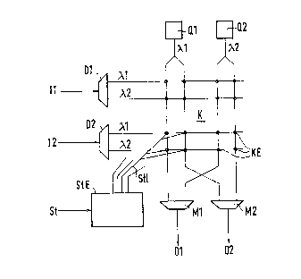
The data switch shown in Fig. 1 has two inputs I1 and
I2, two outputs 01 and 02, two wavelength-division
demultiplexers D1 and D2, two wavelength-division
muLtiplexers M1 and M2, two constant light sources
Q1 and Q2, and a switching matrix K with switching
elements KE.
The switch further includes a control unit StE with
control leads Stl for controlling the switching
elements KE and an external control lead St for
receiving the necessary control signals.
At each input and output, two signals can be transmi~tted
in a wavelength-division multiplex mode. Two operating
wavelengths lambda 1 and lambda 2 are provided. In each
~10~;S39
of the demultiplexers D1 and D2 following the inputs
I1 and I2, a separation according to the two wav-e-
lengths takes place. The four separate sianals are
applied to the row leads of the switching matrix K.
The two constant light sources Q1 and Q2 operate at
the two wavelengths lambda 1 and lambda 2, respec-
tively. Each constant light source feeds two row leads
of the switching matrix K.
The row and column leads intersect at the switching
elements KE. Each switching element KE is designed
to pass the light from the associated constant light
source unaltered in a nonactivated state and to
modulate this light with the signal of the associated
row lead in an activated state. The switching be-
tween the activated and nonactivated states is
effected by the above-mentioned means for controlling
the switching elements.
From each constant light source Q1 and Q2, a column
lead runs to each wavelength-division multiplexer
M1 and M2. The wavelength-division multiplexers M1
and M2 are connected ahead of the outputs 01 and 02,
respectively, and each combine the signals intended
for the respective output, which are modulated onto
light of different operating wavelengths, into a
common wavelength-division-multiplex signal.
Thus, a signal path which is switchable or not
switchable for each signal component coming from the
input by activation or nonactivation of a switching
element KE runs from each input I1 and I2 to each out-
put 01 and 02. By proper selection of the switching elements,
the signal path can be switched with wavelength con-
version (lambda 1/lambda 2, lambda 2/lambda 1) or
without wavelength conversion (lambda 1/lambda 1,
lambda 2/lambda 2). Thus, each signal component
arriving at one of the inputs can be switched to each
of the outputs with or without wavelength conversion,
care normally having to be taken to ensure that for
each operating wavelength, no more than one signal
component is switched to each output, i.e., that
per column lead, no more than one swi~tching element
is activated at a time.
It will be readily apparent to those skilled in the
art that various modifications may be made to the
switch described with the aid of Fig. 1 without de-
parting from the scope of the invention. For example:
Each additional input requires an additional demulti-
plexer, one additional row lead per operating wave-
length, and the associated additional switching
elements.
Each additional output requires one additional column
lead per operating wavelength, the associated
additional switching elements, and one additional
multiplexer.
Each additional operating wavelength requ;res one
additional output and one additional row lead per
demultiplexer, an additional constant light source,
- ~ o ~
an additional column lead from the latter to each
multiplexer, the associated additional switching ele-
ments, and one additional input per multiplexer.
If the optical switch has only one input, it is an
optical demultiplexer. It can be used, for example,
to extract a signal component for an individual sub-
scriber from a multiplex signal circulating in a
ring. In this case, wavelength converters will advantageously
be provided only in the path to this individual subscriber
so as to be able to extract any signal component,but to
offer it to the subscriber always with the same wavelength.
Conversely, the optical switch may have only one out-
put and operate as an optical multiplexer to couple a
signal component from an individual subscriber into,
e.g., a multiplex signal circulating in a ring. In
this case, a wavelength conversion only for the sig-
nal component coming from this subscriber may be
sufficient, and the splitting of the transmitted sig-
nal, and hence the multiplexer at the input, can be
dispensed with.
The control signals from which the signals for driving
the switching elements are derived may also be re-
ceived via the inputs I1 and I2, as is the case in
conventional switches. For this, an additional wave-
length may be used; this corresponds to a separate
control channel in time-division multiplex. The control
signals may also form part of the individual signal
components, e.g., such that each message to be switched
is preceded by control signals.
~a~4~&~
The switching-through of the switching elements may
also be performed dynamically. Thus, in distribution
services, for example, the switch can also perform
the function of a service multiplexer, or simul-
taneous time-division-multiplex switching is possible.
In particular, it is intended to design the switch for
the transfer of ATM signals. Each signal component con-
sists of a sequence of ATM cells which each consist of
a cell header followed by an information part ("payload").
The cell header contains information from which the
remaining path to be taken by the cell can be derived.
From this, as is customary in ATM, control information for
dynamically controlling the switching elements can be
derived. With the aid of this control information, a given
signal path is then switched for the duration of one ATM cell
and, if required, a conversion of the wavelength is
initiated.
The fundamental idea of the invention can be applied
to nearly all structures known from electric time-
division multiplex systems. With the aid of Fig. 2,
this will now be illustrated by the example of a
structure which is totally different from that of
Fig. 1.
The switch of Fig. 2, like that of Fig. 1, has two
inputs I1 and I2, two outputs 01 and 02, two wavelength-
division demultiplexers D1 and D2, and two wavelength-
division multiplexers M1 and M2.
Unlike in the example of Fig. 1, first a supermultiplex
signal is formed. The signal coming from the input I1
2~4~9
is separated by the demultiplexer D1 into signal
components having the operating wavelengthslambda 1
and lambda 2. The signal components are switched
through a switching matrix K1 at one of four wave-
lengths lambda 1, ..., lambda 4 according to their
destination at the outputs. The outputs of the
switching matrix K1 are followed by a wavelength-
division multiplexer MI.1.
Similarly, the demultiplexer D2 associated with the
input I2 is followed by a switching matrix K2 which is
followed by a wavelength-divis;on multiplexer MI2.
Theoutputs of the multiplexers MI1 and MI2 are coupled
to an optical bus B.
The multiplexer M1 ahead of the output 01 is preceded
by a wavelength-division demult;plexer D01. The input
of the latter is connected to the optica-l bus 8. The
wavelength-division demultiplexer D01 has onLy out-
puts for the wavelengths lambda 1 and lambda 2, which
are recombined by the multiplexer M1.
Associated with the output 02 is a wavelength-div;sion
demultiplexer D02 which has outputs for the wavelengths
lambda 3 and lambda 4~ I.n wavelength converters U1 and
U2, the wavelengths lambda 3 and lambda 4 are con-
verted to the wavelengths lambda 1 and lambda 2, re-
spectively, which are recombined by the multiplexer
M2.
2 Q ~
The devices for controlling the sw;tching elements of
the switching matrices K1 and K2 as well as the necessary
constant light sources are not shown here.
For the realization of the individual functions, the person
skilled in the art has sufficient possibilities. For
example, reference is made to an article by M. Sakaguchi
and K. Kaede, "Optical Switching Device Technologies",
IEEE Communications Magazine, May 1987, Vol. 25,
No. 5.
Simple demultiplexers can be implemented with filters,
and simple multiplexers with couplers. Preferred
switching elements are optically controllable and
electrically activatable elements. For the time being,
however, the electric controllability of optical
switches is simpler to implement; to this end, the
input signal components would have to be converted
to electric signals.
From the example of Fig. 2 it is also readily apparent
that a switching matrix can be replaced by tunable
wavelength converters or by connectable and d;scon-
nectable fixed-tuned wavelength converters combined
with optical switches. In that case, the optical
switches must not be designed as modulators in which
the input signal is used only for control purposes.
The switches must be designed so that the opticaL
input signal itself is switched through.
The embodiments given and the possible modifications in-
dicated show that a switch according to the invention
can be implemented in various ways.