Note: Descriptions are shown in the official language in which they were submitted.
/_ 2044707
ADAPTIVE EQUALIZER CAPABLE OF EFFECTIVELY REMOVING
A REMAINING FADING IN AN EQUALIZED SIGNAL
Background of the Invention:
This invention relates to an adaptive equalizer
which is used in combination with a demodulator.
Into a demodulated signal, a demodulator
demodulates a received signal which may be subjected to
fading while transmitted to the demodulator through a
radio channel. The demodulated signal may be a baseband
signal having a binary level or a multilevel. An
adaptive equalizer is supplied with the demodulated
signal and comprises an equalizer section for equalizing
the demodulated signal into an equalized signal in
accordance with a main controllable tap gain and first
through N-th controllable tap gains, where N represents a
positive integer which is not less than one.
A conventional adaptive equalizer further
comprises a producing section for producing a main gain
value and first through N-th gain values dependent upon
the demodulated signal and the equalized signal and a
~ .
2 2 ~ 4 47 0 i
processing section for processing the main gain value and
the first through the N-th gain values into the main
controllable tap gain and the first through N-th
controllable tap gains in accordance with a main
parameter and first through N-th parameters,
respectively.
The main parameter and the first through the N-th
parameters are representative of limiting values for
limiting the main gain value and the first through the
N-th gain values, respectively. The limiting values are
used in rapidly controlling the main controllable tap
gain and the first through the N-th controllable tap
gains.
The conventional adaptive equalizer is disclosed
in an article contributed by Hajime Yamamoto and Takaya
Endo to the ELECTRICAL COMMUNICATION LABORATORIES
TECHNICAL JOURNAL, VOL. 23 No. 6 of Nippon Telegraph and
Telephone Public Corporation in 1974, pages 1115 to 1149,
under the title of "Automatic Equalizer in 1.544 Mb/s
PCM-FDM System". In the conventional adaptive equalizer,
the main parameter is equal to one. The first through
the N-th parameters are less than the main parameter.
However, the first through the N-th parameters
are not varied in accordance with the demodulated signal
in the conventional adaptive equalizer on controlling the
main controllable tap gain and the first through the N-th
controllable tap gains. As a result, the fading
partially remains a6 a remaining fading in the equalized
2044707
_
3 64768-245
signal. Therefore, lt is dlfflcult to effectlvely remove the
remalnlng fadlng ln the equallzed slgnal.
Summary of the Inventlon
It ls an ob~ect of thls lnventlon to provlde an
adaptlve equallzer capable of produclng an equallzed slgnal
whlch lncludes substantlally no remalnlng fading.
Other ob~ects of thls lnventlon wlll become clear as
the descrlptlon proceeds.
On descrlblng the glst of thls lnventlon, lt ls
posslble to understand that an adaptive equalizer is connected
to a demodulator for demodulating a recelved signal into a
demodulated signal. The adaptive equallzer comprises an
equallzer section for equallzlng the demodulated slgnal lnto an
equalized slgnal ln accordance with a main controllable tap gain
and flrst through N-th gain values dependent upon the
demodulated slgnal and the equallzed slgnal, and a llmitlng
sectlon for llmltlng said maln galn value and sald flrst through
said N-th galn values ln accordance wlth a maln parameter and
flrst through N-th parameters, respectlvely, to produce sald
maln controllable tap galn and sald flrst through said N-th
controllable tap galns.
Accordlng to thls lnventlon, the above-understood
adaptlve equallzer further comprlses (A) detectlng means for
detectlng whether or not the demodulator ls ln a
_ 2~4~7
4 64768-245
carrler synchronization state, the detectlng means produclng a
first detectlng signal when the demodulator is into the carrier
synchronizatlon state, the detectlng means producing a second
detecting signal when the demodulator is out of the carrler
synchronlzatlon state, (B) first supplying means responslve to
any one of the first and the second detecting signals for
supplying a main value as the main parameter to the processlng
section, (C) second supplying means responsive to the first
detecting signal for supplying first through N-th values as the
first through the N-th parameters to the processing section,
respectively, the second supplying means being responsive to the
second detecting signal for supplying first through N-th
additional values as the first through the N-th parameters to
the processing section, respectively.
Brief Description of the Drawinqs
Fig. 1 is a block diagram of a conventional adaptlve
equallzer;
Fig. 2 is a block dlagram of a correlatlon circuit
used in the adaptive equalizer illustrated in Fig. 1;
Flg. 3 is a block diagram of a limiting circuit used
in the adaptive equallzer illustrated ln Flg. 1;
Flg. 4 ls a slgnature curve of a recelver whlch
comprlses the adaptlve equallzer lllustrated in Fig. 1;
Fig. 5 is a block diagram of an adaptive equalizer
according to an embodiment of this lnventlon;
'
20 1 1707
Fig. 6 is a block diagram of a limiting value
controlling circuit used in the adaptive equalizer
illustrated in Fig. 5i
Fig. 7 is a signature curve of a receiver which
comprises the adaptive equalizer illustrated in Fig. 5;
Fig. 8 is a block diagram of another limiting
value controlling circuit used in the adaptive equalizer
illu~trated in Fig. 5; and
Fig. 9 is a block diagram of still another
controlling circuit used in the adaptive equalizer
illustrated in Fig. 5.
Description of the Preferred Embodiment:
Referring to Fig. 1, description will first be
made as regards a conventional adaptive equalizer 11 for
a better understanding of this invention. The adaptive
equalizer 11 has equalizer input and output terminals 12
and 13. The input terminal 12 is connected to a
demodulator section 14. Through a radio channel, a
transmitted signal is supplied to the demodulator section
14 as a received signal which is subjected to fading
while transmitted to the demodulator section 14 through
the radio channel. The transmitted signal may be, for
example, a modulated signal into which a carrier signal
is modulated by a digital signal. The digital signal is
produced by sampling an analog signal at a sampling
frequ~ncy f. The analog signal may be a speech signal.
The demodulator section 14 demodulates the
received signal into a demodulated signal to supply the
20~7C7
demodulated signal to the input terminal 12 of the
adaptive equalizer 11. The demodulated signal may be a
baseband signal having a binary level or a multilevel.
The adaptive equalizer 11 is for equalizing the
demodulated signal into an equalized signal for supplying
the output terminal 13 with the equalized signal. In the
adaptive equalizer 11, a transversal filter 15 is for
filtering the demodulated signal into a filtered signal
in accordance with a main controllable tap gain and first
through N-th controllable tap gains, where N repre~ents a
positive integer which is not less than one. The
filtered signal is equal to the equalized signal. In the
illustrated example, the positive integer N is equal to
two.
lS The main controllable tap gain and the first and
second controllable tap gains are supplied from a tap
gain control circuit 16 to the transversal filter 15.
The transversal filter 15 comprises first and
second delay circuits (D) 17-1 and 17-2 and a main filter
multiplier 18-0 and first and second filter multipliers
18-1 and 18-2. Each of the first and the second delay
circuits 17-1 and 17-2 gives a delay of a predetermined
time (l/f) to a signal supplied thereto. The demodulated
signal is supplied to the first filter multiplier 18-1.
The first and the second delay circuits 17-1 and 17-2
supply first and second delayed signal to the main filter
multiplier 18-0 and second filter multiplier 18-2,
respectively.
~,
204470 ~
Supplied with the first controllable tap gain in
the manner which will be described hereinafter, the first
filter multiplier 18-1 multiplies the demodulated signal
by the first controllable tap gain to supply a first
multiplied signal to a filter adder 19. The main filter
multiplier 18-0 and the second filter multiplier 18-2
multiply the first and the second delayed 6ignals by the
main controllable tap gain and the second controllable
tap gain to ~upply main and second multiplied signals to
the filter adder 19, respectively. The filter adder 19
calculates a total sum of the main, the first, and the
second multiplied signals to supply the total sum as the
equalized signal to the output terminal 12 and the tap
gain control circuit 16.
The tap gain control circuit 16 comprises a
correlation circuit 20 and main, first, and second
limiting circuits 21-0, 21-1, and 21-2. The correlation
circuit 20 receives the demodulated signal and the
equalized signal.
Referring to Fig. 2, the correlation circuit 20
is for producing a main gain value and first and second
gain values in accordance with the demodulated signal and
the equalized signal. The correlation circuit 20
comprises a subtracter 22 and first and second
correlation delay circuits 23-1 and 23-2. The subtracter
22 subtracts the equalized signal from the demodulated
signal to deliver an error signal to main, first, and
second correlation multipliers 24-0, 24-1, and 24-2,
2044707
respectively. Each of the first and the second
correlation delay circuits 23-1 and 23-2 gives a delay of
the predetermined time (l/f) to a signal supplied
thereto. The fir8t and the second correlation delay
circuits 23-1 and 23-2 supply first and second
correlation delayed signals to the main and the second
correlation multipliers 24-0 and 24-2, respectively. The
main correlation multiplier 24-0 multiplies the first
correlation delayed signal by the error signal to supply
a main correlation multiplied signal to a main integrator
25-0. The first and the second correlation multipliers
24-1 and 24-2 multiply the demodulated signal and the
second correlation delayed signal by the error 6ignal,
respectively. The first and the second correlation
multipliers 24-1 and 24-2 supply first and second
correlation multiplied signals to first and second
integrators 25-1 and 25-2, respectively. The main, the
first, and the second integrators 25-0, 25-1, and 25-2
successively integrate the main, the first, and the
second correlation multiplied signals into main, first,
and second integrated signals, respectively. The main,
the first, and the second integrators 25-0, 25-1, and
25-2 supply the main, the first, and the second
integrated signals to the main, the first, and the second
limiting circuits 21-0, 21-1, and 21-2 as the main, the
first~ and the second gain values, respectively.
Referring to Fig. 3 in addition to Fig. 1, the
main, the first, and the second limiting circuits 21-0,
2G44707
21-1, and 21-2 are for limiting the main, the first, and
the second gain values in accordance with main, first,
and second limiting values, respectively, on producing
the main, the first, and the second controllable tap
gains. The main, the first, and the second limiting
values are positive values, respectively, and may be
different from each other.
The first limiting circuit 21-1 comprises a first
limiting value generator 26, an absolute calculator 27, a
judging circuit 28, a comparator 29, an inverting circuit
30, and first and second selecting circuits 31 and 32.
In the illustrated example, each of the main and the
second limiting circuits 21-0 and 21-2 comprises similar
parts which are illustrated in Fig. 3.
Supplied with the first gain value, the absolute
calculator 27 calculates the absolute value of the first
gain value to deliver a first absolute value to the
comparator 29. The judging circuit 28 judges whether or
not the first gain value has a negative value. The
2~ judging circuit 28 produces a first positive signal when
the first gain value does not have the negative value.
When the first gain value has the negative value, the
judging circuit 28 produces a first negative signal. The
first limiting value generator 26 generates the first
limiting value. Supplied with the first absolute value
and the first limiting value, the comparator 29 compares
the first absolute value with the first limiting value.
The comparator 29 produces a first judge result signal to
20~707
-
supply a first judge result signal to the second
selecting circuit 32 when the fir~t ab~olute value i~
smaller than the first limiting value. When the first
absolute value is not smaller than the first limiting
value, the comparator 29 produces a fir~t detection
signal to supply the first detection signal to the second
selectinq circuit 32.
The inverting circuit 30 inverts the polarity of
the first limiting value to produce a first inverted
limiting value, i.e. a negative limiting value. The
first inverted limiting value is delivered to the first
selecting circuit 31. The first selecting circuit 31
receives the first inverted limiting value together with
the first limiting value. Responsive to the first
positive signal, the first selecting circuit 31 selects
the first limiting value from the first inverted limiting
value and the first limiting value to supply the first
limiting value to the second selecting circuit 32 as a
first selected value. Responsive to the first negative
~ignal, the first selecting circuit 31 selects the first
inverted limiting value from the first inverted limiting
value and the first limiting value to supply the first
inverted limiting value to the second selecting circuit
32 as the first selected value. The second selecting
circuit 32 receives the first selected value together
with the first gain value. Responsive to the first judge
result signal, the second selecting circuit 32 selects
the first gain value from the first selected value and
11 20 147~7
; the fir~t gain value to supply the first gain value to
the transversal filter 15 a~ the first controllable tap
gain. Responsive to first detection signal, the 8econd
selecting circuit 32 selects the first selected value
from the first selected value and the first gain value to
supply the first selected value to the transversal filter
15 as the first controllable tap gain. Similarly, the
main and the second limiting circuits 21-0 and 21-2
process the main and the second gain values into the main
and the second controllable tap gain~ in accordance with
the main and the second limiting values, respectively.
In the conventional adaptive equalizer, the main
limiting value is equal to a predetermined value which
is, for example, equal to 1. Each of the first and the
second limiting values is equal to a prescribed value
which is not greater than the predetermined value and may
be, for example, equal to 1/2. When the main limiting
value is equal to 1 and each of the first and the second
limiting values is equal to 1/2, it is possible to
rapidly control the main controllable tap gain and the
first and the second controllable tap gains. However,
fading remains as a remaining fading in the equalized
signal in the conventional adaptive equalizer. Namely,
it is difficult to effectively remove the remaining
fading in the equalized signal.
The conventional adaptive equalizer takes a long
time to control the main and the first through the N-th
controllable tap gains into optimum tap gains,
12 20~A707
respectively, when the main and the first through the
N-th controllable tap gains are greatly apart from the
optimum tap gains, namely, when a remaining distortion is
left in the equalized signal. It often becomes
impossible to control the main and the first through the
N-th controllable tap gains into optimum tap gain~,
respectively, when the demodulator section is put out of
the carrier synchronization state.
It iB necessary to render the main and the first
through the N-th controllable tap gains into great
values, respectively, in order to remove a serious fading
from the equalized signal when the serious fading occurs
in the radio channel. In the conventional adaptive
equalizer, absolute values of the main and the first
through the N-th controllable tap gains are restricted
within limiting values, respectively. As a result, the
absolute values of the main and the fir~t through the
N-th controllable tap gains must become over the limiting
values in order to remove the fading when the fading
becomes great. However, the absolute value6 of the main
and the first through the N-th controllable tap gains are
restricted within limiting values, respectively.
Fig. 4 shows a signature curve as called in the
art. In order to describe the signature curve a little
more in detail, attention will be directed to the fact
that the conventional adaptive equalizer 11 is used in a
receiver comprising the demodulator section 14. The
signature curve is had by the receiver and is for use in
2 0~47 ~ ~
13
estimating an efficiency of the receiver in connection
with the fading. In Fig. 4, the signature curve
represents depths (Dn) of notches in dB as regards notch
frequencies (fn) in MHz of the fading when the equalized
signal has an error rate (Pe) of 1 x 10 4.
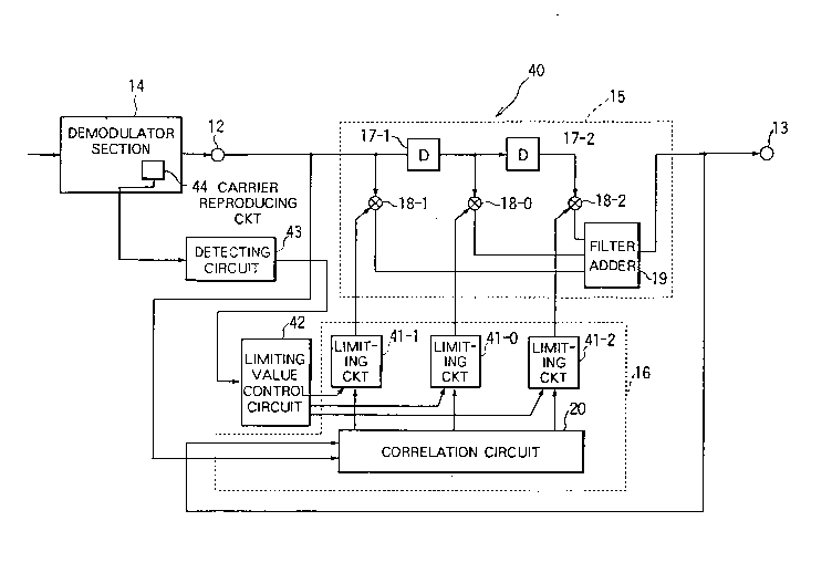
Referring to Fig. 5, the description will proceed
to an adaptive equalizer according to a preferred
embodiment of this invention. The illustrated adaptive
equalizer is different in structure from the adaptive
1~ equalizer 11 illustrated with reference to Fig. 1 and is
therefore designated afresh by a reference numeral 40.
The adaptive equalizer 40 comprises similar parts which
are designated by like reference numerals and are
operable with likewise named signals. The adaptive
equalizer 40 comprises main, first, and second limiting
circuits which are different from the main, the first,
and the second limiting circuits 21-0, 21-1, and 21-2
illustrated in Fig. 1 and which are therefore designated
by different reference numerals 41-0, 41-1, and 41-2,
respectively. The adaptive equalizer 40 further
comprises a limiting value control circuit 42 and a
detecting circuit 43.
The demodulator section 14 comprises a carrier
reproducing circuit 44 for reproducing the carrier signal
in synchronism with the received signal. When the
carrier signal is reproduced from the received signal,
the carrier reproducing circuit 44 produces a first
control signal to supply the first control signal to the
~ 20447~7
14 64768-245
detecting clrcult 43. When the carrler slgnal ls not
synchronlzed wlth the recelved slgnal, the carrler reproduclng
clrcult 44 supplles a second control slgnal to the detectlng
clrcult 43. The detectlng clrcult 43 dlscloses ln Japanese
Unexamlned Patent Publlcation No. 17661/1973 (Tokkai Syo 48-
17661 whlch was published on March 6, 1973).
When supplied with the first control signal, the
detecting clrcuit 43 knows that the demodulator section 14 is
put in a carrier synchronization state. The detecting circuit
43 delivers a synchronization signal to the llmltlng value
control clrcult 42. When supplled wlth the second control
slgnal, the detectlng clrcult 43 knows that the demodulator
sectlon 14 is put out of the carrier synchronization state. The
detecting circuit 43 delivers a non-synchronization slgnal to
the limiting value control circult 42.
Referring to Figure 6 together with Flgure 5, the
llmlting value control circuit 42 comprises a main generator 45-
0 and first and second subsidiary generators 45-1 and 45-2. The
main generator 45-0 and the first and the second subsidiary
generators 45-1 and 45-2 generate a main value signal and first
and second subsidiary value signals, respectively. In the
illustrated example, the main value signal is representative of
1. The flrst and the second subsldlary value slgnals are
representative of 1 and l/2, respectively. The main value
signal is supplied to the maln limiting circuit 41-0 as a main
parameter. The first and the second subsidiary value
,
-~ 2 0447 0~
signals are delivered to a limiting ~elector 46 which is
selectively given the synchronization and the
non-synchronization signals. When supplied with the
synchronization signal, the limiting selector 46 selects
the first subsidiary value signal from the first and the
second subsidiary value signals to supply the first
subsidiary value signal to the first and the second
limiting circuits 41-1 and 41-2 as first and second
parameters, respectively. When supplied with the
non-synchronization signal, the limiting selector 46
selects the second subsidiary value signal from the fir~t
and the second subsidiary value signals to supply the
second subsidiary value signal to the first and the
second limiting circuits 41-1 and 41-2 as first and
second parameters, respectively.
In Fig. 5, the first limiting circuit 41-1 is
similar in structure to that de~cribed in conjunction
with Fig. 3 except that the first limiting value
generator 26 is omitted from Fig. 5. The first
subsidiary value signal is supplied from the limiting
value control circuit 42 to the first limiting circuit
41-1 as the first parameter when the demodulator section
14 is put in the carrier synchronization state.
Similarly, the second subsidiary value signal is supplied
from the limiting value control circuit 42 to the first
limiting circuit 41-1 as the first parameter when the
demodulator section 14 is put out of the carrier
synchronization state. Therefore, the first limiting
- 2044707
, .
16
circuit 41-1 processes the first gain value into the
first controllable tap gain in accordance with the first
parameter.
Each of the main and the second limiting circuits
41-0 and 41-2 comprises parts which are similar to those
of the first limiting circuit 41-1. The main value
signal i8 supplied from the limiting value control
circuit 42 to the main limiting circuit 41-0 a~ the main
parameter when the demodulator section 14 i8 either put
in or out of the carrier synchronization state. The main
limiting circuit 41-0 processes the main gain value into
the main controllable tap gain in accordance with the
main parameter.
The first subsidiary value signal is supplied
from the limiting value control circuit 42 to the second
limiting circuit 41-2 as the second parameter when the
demodulator section 14 iB put in the carrier
synchronization state. Similarly, the second subsidiary
value signal is supplied from the limiting value control
circuit 42 to the second limiting circuit 41-2 as the
second parameter when the demodulator section 14 iB put
out of the carrier synchronization state. Therefore, the
~econd limiting circuit 41-2 processes the second gain
value into the second controllable tap gain in accordance
with the second parameter.
Referring to Fig. 7, a signature curve iB similar
to that shown in Fig. 4 and shows a characteristic of a
receiver comprising the adaptive equalizer 40 illustrated
:
2 04~ 7 0 ~
17
in Fig. 5. In Fig. 7, the depth (Dn) of the notch i8
equal to about 25 dB when the notch frequency (fn) i8
equal to 0 MHz. The depth (Dn) of the notch is equal to
about 24 dB when the notch frequencies (fn) are equal to
+5 MHz and -5 MHz. For reference, the depth (Dn) of the
notch is equal to about 23 dB when the notch frequency
(fn) is equal to 0 MHz in Fig. 4. The depth (Dn) of the
notch is equal to about 20 dB when the notch frequencies
(fn) are equal to +5 MHz and -5 MHz in Fig. 4. by
ln comparing Figs. 4 and 7, it is readily understood that
the adaptive equalizer according to this embodiment is
superior in characteristic to the conventional adaptive
equalizer illustrated in Fig. 1.
In the adaptive equalizer illustrated in Fig. 5,
it often becomes difficult to control the main, the
first, the second controllable tap gains in case where
the first and the second parameters rapidly turn 1/2 to 1
when the demodulator section 14 rapidly turn the carrier
synchronization state to non carrier synchronization
state.
Referring to Fig. 8 in addition to Fig. 5,
description will be made as regards another example of a
limiting value control circuit. The illu~trated limiting
value control circuit is different in structure from the
limiting value control circuit 42 illustrated in Fig. 6
and is,therefore designated afresh by a reference numeral
50. The limiting value control circuit 50 comprises a
main value generator 51 and a subsidiary value generator
2~ 707
,,_
18
52. Supplied with any one of the synchronization and the
non-synchronization signals, the main value and the
subsidiary value generators 51 and 52 generate main and
subsidiary value signals which are representative of main
and subsidiary values, respectively. The main and the
subsidiary values are equal, for example, to 1 and 1/2,
respectively.
The limiting value control circuit 50 further
comprises an up counter circuit 53 connected to the
detecting circuit 43. The up counter circuit 53 has an
enable terminal labelled "EN", a reset terminal labelled
"RT", a clock input terminal labelled "CLK", a count up
terminal labelled "UP", and a signal output terminal
labelled "ST". The up counter circuit 53 is connected to
a gate circuit 54 through the clock input terminal CLK
and the count up terminal UP. The gate circuit 54 is
further connected in turn to a clock oscillator 55. The
gate circuit 54 is operable to selectively supply clock
pulse~ from the clock o~cillator 55 to the up counter
circuit 53. The gate circuit 54 stops supplying the
clock pulses to the up counter circuit 53 in response to
a carry signal which will presently be described.
A~ de~cribed above in conjunction with Fig. 5,
the detecting circuit 43 supplies the synchronization
signal to the limiting value control circuit 50 when the
demodulator section 14 is put in the carrier
synchronization state. When the demodulator section 14
is put out of the carrier synchronization state, the
2~4A7 0~
19
detecting circuit 43 supplies the non-synchronization
signal to the limiting value control circuit 50. The
synchronization and the non-synchronization signal~ may
be high and low level signals, respectively.
Referring to Fig. 8 alone, the up counter circuit
53 has an initial count which may be equal to zero. When
supplied ~ith the synchronization 6ignal from the enable
terminal EN, the up counter circuit 53 counts up the
clock pulse6 to produce a count. From the signal output
terminal ST, the up counter circuit 53 supplies a
limiting multiplier 56 with a count signal which i~
representative of the count. When the count reaches a
predetermined number M such as 21, the up counter
circuit 53 supplies the carry signal to the gate circuit
54 through the count up terminal UP. Responsive to the
carry signal, the gate circuit 54 stops supplying the
clock pulses to the counter circuit 53. The up counter
circuit 53 continues supplying the limiting multiplier 56
with the count signal which is representative of the
predetermined number M.
Supplied with the non-synchronization signal from
the detecting circuit 43, an inverter gate 57 inverts the
~ynchronization signal into an inverted signal to supply
the inverted signal to the up counter circuit 53. When
supplied with the inverted signal at the reset terminal
RT, tpe up counter circuit 53 is reset into the initial
count and stop~ supplying the carry signal to the gate
circuit 54. As a result, the gate circuit 55 serve~ to
~ ~ 20~707
selectively supply the clock pulse~ to the counter
circuit 53.
As described above, the count signal is supplied
to the limiting multiplier 56. The limiting multiplier
56 is connected to a coefficient generator 58 for
generating a coefficient ~ignal representative of a
predetermined coefficient K. The predetermined
coefficient K is given by:
K - (P - Q)/M, (1)
where P represents the main value and Q represent~ the
6ubsidiary value.
The limiting multiplier 56 multiplies the count
signal by the coefficient signal to supply a limiting
multiplied signal to a limiting adder 59. The limiting
multiplied Bignal i6 RUpplied together with the
subsidiary value signal to the limiting adder 59. The
limiting adder S9 adds the subsidiary value signal to the
limiting multiplied signal to produce a sum signal. The
limiting adder 59 supplies the ~um signal to the first
and the second limiting circuits 41-1 and 41-2 (Fig. 5)
as the fir~t and the second parameters, re~pectively.
The main value signal is supplied from the main value
generator 51 to the main limiting circuit 41-0 (Fig. 5)
as the main parameter.
In conjunction with Fig. 8, it i8 readily
under~tood that the up counter circuit 53, the limiting
multiplier 56, the coefficient generator 58, and the
limiting adder 59 are collectively operable as a ~ending
21 204~70~
circuit.
Referring to Fig. 9 in addition to Fig. 5,
description will proceed to a still another example of a
limiting value control circuit. The illu~trated limiting
value control circuit is different from the limiting
value control circuit 50 illustrated in Fig. 8 and is
therefore designated afresh by a reference numeral 60.
The limiting value control circuit 60 comprises similar
parts which are designated by like reference numerals and
are operable by likewise named 6ignals. The limiting
value control circuit 60 comprises an up/down counter
circuit 61 having an initial count which may be equal to
zero. The up/down counter circuit 61 has an enable
terminal labelled "EN", a first signal input terminal
labelled "U", a second signal input terminal labelled
"D", a clock input terminal labelled "CLK", a count up
terminal labelled "UP", a count down terminal labelled
"DN", and a signal output terminal labelled "ST".
The up/down counter circuit 61 i6 directly
connected to the clock oscillator 55 at the clock input
terminal CLK. The clock 06cillator 55 6upplies clock
pulses to the up/down counter circuit 61. The up/down
counter circuit 61 is selectively operable as up and down
counters. When the up/down counter circuit 61 is
operable as the up counter, the up/down counter circuit
61 counts up the clock pulses to produce a fir~t count
signal representative of a first count. When the first
count reaches the predetermined count number M, the
~ 2044707
22
up/down counter circuit 61 produces a carry signal from
the count up terminal UP. The carry signal has a high
level. When the up/down counter circuit i8 operable as
the down counter, the up/down counter circuit 61 counts
down the clock pulses to produce a ~econd count ~ignal
representative of a second count. When the second count
reaches the initial count, the up/down counter circuit 61
produces a borrow signal from the count down terminal DN.
The borrow signal has a high level~
ln When the demodulator section 14 i8 put in the
carrier synchronization state, the detecting circuit 43
supplies the limiting value control circuit 60 with the
synchronization signal which i~ the high level signal.
When ~upplied with the synchronization signal at the
first signal input terminal U, the up/down counter
circuit 61 is operable as the up counter. The
~ynchronization signal is further supplied to a primary
inverter gate 62 and a first AND gate 63-1. The primary
inverter gate 62 inverts the synchronization signal into
a first inverted signal of a low level to supply the
first inverted signal to a second AND gate 63-2. When
the up/down counter circuit 61 produces neither the carry
~ignal or the borrow ~ignal, the fir~t and the second AND
gates 63-1 and 63-2 supply a NOR gate 64 with first and
second AND'ed signals, each representative of the low
level. The NOR gate 64 supplie~ the enable terminal EN
of the up/down counter circuit 61 with a first NOR'ed
signal having a high level. When supplied wit~ the first
~~ 23 20 1 4707
NOR'ed signal, the up/down counter circuit 61 counts up
the clock pulses to supply the limiting multiplier 56
with the first count signal.
In the similar manner described in conjunction
with Fig. 8, the limiting multiplier 56 multiplies the
first count signal by the coefficient ~ignal to supply a
first limiting multiplied signal to the limiting adder
59. The limiting adder 59 adds the first limiting
multiplied signal to the subsidiary value signal to
produce a first sum signal. The limiting adder 59
supplies the first sum signal to the first and the second
limiting circuits 41-1 and 41-2 as the first and the
second parameters, respectively.
As described above, the up/down counter circuit
61 produces the carry signal when the first count signal
is representative of the predetermined number M. As a
result, the first AND gate 63-1 ~upplies the NOR gate 64
with a third AND'ed signal having a high level. Inasmuch
as the second AND gate 63-2 supplies the second AND'ed
signal to the NOR gate 64, the NOR gate 64 supplies the
enable terminal EN of the up/down counter circuit 61 with
a second NOR'ed signal having a low level. When supplied
with the second NOR'ed signal through the enable terminal
EN, the up/down counter circuit 61 stops the count up
operation and continues supplying the limiting multiplier
56 with the first count signal having the predetermined
number M.
When the demodulator section 14 is put out of the
2044 70~
24
carrier synchronization state, the detecting circuit 43
. supplies the limiting value control circuit 60 with the
~ non-synchronization 6ignal which i~ the low level signal.
The non-synchronization signal is supplied to the primary
inverter gate 62 and the first AND gate 63-1. The
primary inverter gate 62 invert~ the non-synchronization
signal into a second inverted signal having a high level.
The primary inverter gate 62 supplies the second inverted
signal to the second AND gate 63-2 and the second signal
input terminal D. When supplied with the ~econd inverted
signal through the second signal input terminal D, the
up/down counter circuit 61 is operable as the down
counter.
When supplied with the non-synchronization
signal, the first AND gate 63-1 supplies the fir~t AND'ed
signal to the NOR gate 64. Inasmuch as the up/down
counter circuit 61 does not produce the borrow signal,
the second AND gate 63-2 supplies the ~econd AND'ed
signal to the NOR gate 64. The NOR gate 64 supplie6 the
first NOR'ed signal to the enable terminal EN of the
up/down counter circuit 61. When supplied with the first
NOR'ed signal, the up/down counter circuit 61 count~ down
the clock pulses to supply the limiting multiplier 56
with the second count signal~
In the manner described in conjunction with Fig.
8, the limiting multiplier 56 multiplies the second count
signal by the coefficient signal to supply a ~econd
limiting multiplied signal to the limiting adder 59. The
20~470~
; 25
limiting adder 59 adds the limiting multiplied signal to
the subsidiary value signal to produce a second sum
signal. The limiting adder 59 supplies the ~econd sum
signal to the first and the second limiting circuits 41-1
and 41-2 as the first and the second parameters,
respectively.
As described above, the up/down counter circuit
61 produces the borrow signal having a high level when
the second count ~ignal represent~ the initial count. As
1~ a result, the second AND gate 63-2 ~upplies the NOR gate
64 with a fourth AND'ed signal having a high level. The
NOR gate 64 ~upplies the second NOR'ed signal to the
enable terminal EN of the up/down counter circuit 61.
Responsive to the second NOR'ed signal, the up/down
counter circuit 61 stops the count down operation and
continues supplying the limiting multiplier 56 with the
second count signal having the initial count.
In conjunction with Fig. 9, it is readily
understood that the up/down counter 61, the limiting
multiplier 56, the coefficient generator 58, and the
limiting adder 59 collectively serve a~ a sending
circuit.
As described above in conjunction with Figs. 8
and 9, it is possible to sufficiently control the main,
the first, and the second controllable tap gains because
the ~irst and the second parameters gradually increase
from the subsidiary value to the main value.