Note: Descriptions are shown in the official language in which they were submitted.
NE-342 2~45338
TITLE OF THE INVENTION
2 UClock Recovery Circuit With Open-Loop Phase Estimator
3 And Wideband Phase Tracking Loop"
4 BACKGROUND OF THE INVENTION
s The present invention relates generally to APSK (amplitude and
6 phase shift keyed) modulation receivers, and more specifically to a clock
7 recovery circuit for APSK signals.
8 As described in H. Tomita et al "Preambleless Demodulator For
9 Satellite Communications," open-loop phase estimation is known for
10 detecting a phase difference between transmitted clock and local clock.
11 Such open-loop phase estimation is implemented with envelope
12 detection, phase correlation, low-pass filtering and arctangent calculation.
13 While satisfactory for detecting a phase difference during the period of a14 short packet, the phase estimation technique is not capable of tracking
slow phase variations which may occur during a continuous transmission.
16 Another technique which has been extensively used for recovering clock
17 timing is the phase locked loop implemented by a phase detector, a
18 loop filter, and a voltage controlled oscillator. An analog-to-digital
19 converter is clocked by the VCO for sampling a received APSK signal and
supplying the samples to the phase detector in which the phase
21 difference between the sampling clock and the transmitted clock is
22 detected. However, the PLL approach takes long to establish clock
2 3 synchronization.
24 SUMMARY OF THE INVENTION
2 5 It is therefore an object of the present invention to provide a clock
26 recovery circuit capable of establishing clock synchronization in a short,27 invariable length of time.
28 The object of the present invention is obtained by a quasi-open loop
29 clock recovery circuit formed by an open loop phase estimator and a
~3
NE-342 2045~38
wideband phase tracking loop.
2 According to the present invention, there is provided a clock
3 recovery circuit which comprises a clock source for generating a first
4 clock at a frequency N times higher than the clock frequency of a
5 received APSK signal. An A/D (analog-to-digital) converter samples the
6 orthogonal APSK signals in response to the first clock and quantizes the
7 APSK samples into orthogonal digital APSK samples. An envelope
8 detector is coupled to the A/D converter for generating a signal
9 representative of the envelope of the orthogonal APSK digital samples.
10 From the first clock orthogonal sinusoidal signals are derived having a
1 1 frequency which is 1/N of the frequency of the clock. Phase correlations
12 are detected between the orthogonal sinusoidal signals and the envelope
13 representative signal for coupling to a low-pass filter in which the phase
14 correlations are averaged. An arctangent calculator is coupled to the
15 low-pass filter for calculating the arctangent between the low-pass filtered
16 orthogonal signals. A frequency divider is connected to the clock source
17 for generating a second clock at a frequency which is 1/N of the
18 frequency of the first clock. A phase difference is detected by a phase
19 comparator between the second clock and a sample clock which is
20 generated at a frequency 1/N of the frequency of the first clock by a
21 digital voltage-controlled oscillator, the phase difference being applied to
22 a subtracter in which it is subtracted from the output of the arctangent
23 calculator. A threshold comparator is provided for comparing the output
24 of the subtracter with N successive reference values for generating one of
25 N output values respectively corresponding to the N reference values if
26 the output of subtracter corresponds to one of the reference values. The
27 reference values are preferably given by (2~/N) x M, where M is an
2 8 integer in the range between 1 and N. In response to the first clock, the
29 digital V.C.O. controls the timing of the sample clock N times during the
NE-342 2 0 4 ~ 3 3 8
interval between successive sampling instants in accordance with the
2 output of the threshold comparator. The sample clock is applied to a
3 sampler for sampling the digital samples from the A/D converter.
4 In a preferred embodiment, an interpolator is coupled to the output
S of the sampler for receiving samples therefrom in response to the sample
6 clock from the V.C.O. as candidate values and interpolating a sample
7 which may exist between the candidate values in accordance with the
8 output of the subtracter.
9 BRIEF DESCRIPTION OF THE DRAWINGS
The present invention will be described in further detail with reference
11 to the accompanying drawings, in which:
12 Fig. I is a block diagram of an APSK demodulator according to a first
13 embodiment of the present invention; and
14 Fig. 2 is a block diagram of an APSK demodulator according to a
second embodiment of the present invention.
1 6 DETAILED DESCRIPTION
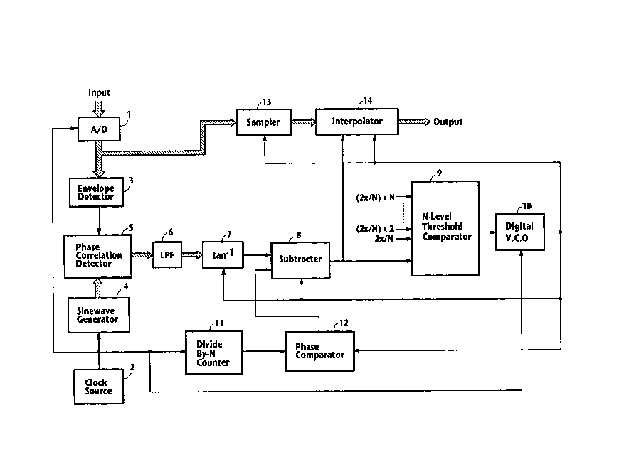
17 Referring now to Fig. 1, there is shown an APSK (amplitude and
18 phase shift keying) demodulator incorporating a clock recovery circuit
19 according to a first embodiment of the present invention.
An amplitude and phase shift keyed signal from a transmitting site is
21 received and orthogonally detected to produce an orthogonal APSK
22 signal, which is applied to an analog-to-digital converter 1. A/D
23 converter 1 samples the APSK signal at intervals Ts of the clock supplied
24 from a clock source 2 and quantizes the samples into a multibit digital
signal of complex value. The frequency fs of the clock source 2 is N
2 6 (where N is an integer) times higher than the frequency fc of the
27 transmitted clock. An envelope detector 3 is coupled to the output of
28 A/D converter 1 to derive a signal X(nTS) representative of the envelope
29 of the transmitted carrier (where Ts = 1/fs).
NE-342 204~338
- 4 -
To the clock source is connected a sinewave generator 4 which may
2 be implemented with a read-only memory in which orthogonal
3 instantaneous values of a sinusoidal waveform are stored and a counter
4 for counting the clock to produce a binary count. The binary count is
s applied to the ROM as an address signal to generate orthogonal versions
6 of a sinusoid having a frequency 1 /N of the clock frequency fs.
7 The outputs of the envelope detector 3 and sinewave generator 4 are
8 coupled to a phase correlation detector 5 in which their relative phase
9 correlation is detected to produce a phase correlation output of complex
value which is given by Y(nTS) = X(nTS) exp{j27~ffs/N)nTs}, (where n = 0,
1 1 1 , 2).
12 The phase correlation output is applied to a digital low-pass filter 6 in
13 which it is averaged out over time and fed into an arctangent calculator 714 in response to a sample clock supplied from a digital voltage-controlled
1 s oscillator 10 at intervals Tc (where Tc is equal to 1 /fc and is 1 /N of the
16 clock intervals Ts). At intervals Tc, arctangent calculation is performed by
17 arctangent calculator 8 between the real and imaginary components of
18 the complex values to produce a signal representative of the phase
19 difference between the clock frequency of the incoming signal and the
local clock frequency. The output of arctangent calculator 7 is coupled to
21 a subtracter 8 to which the output of a phase comparator 12 is also
22 applied.
23 The output of subtracter 8 is compared by an N-level threshold
24 comparator 9 with successive reference values represented by 2~/N,
(2~/N) x 2, (27~/N) x 3, .. 2~/N. If the instantaneous value of the signal
2 6 from subtracter 8 falls in one of the amplitude intervals between
27 successive reference values, the comparator 9 produces a digital signal
28 representing that interval.
29 The output of threshold comparator 9 is applied as a phase control
NE-342 204~338
signal to a digital voltage-controlled oscillator 10 which is clocked at
2 intervals Ts by clock source 2 to generate a sampling clock frequency fc
3 whose phase timing is determined at intervals Ts in accordance with the
4 output of threshold comparator 9.
s A divide-by-N counter 11 is connected to clock source 2 to divide its
6 frequency by a factor N to produce a sampling clock at intervals Tc,
7 which is applied to the phase comparator 12 for making a phase
8 comparison with the output of digital V.C.O. 10.
9 The difference between the outputs of arctangent calculator 7 and
l o phase comparator 12 is detected by subtracter 8, compared with
11 successive threshold values by comparator 9. The output of comparator
12 9 indicates a phase error of the fc sample clock. At source clock intervals
13 Ts, voltage-controlled oscillator 10 controls the phase angle of the fc
14 sampling clock according to the output of subtracter 9 and recovers the
transmitted clock timing.
16 More specifically, the range of signals which appear at the output of
17 subtracter 8 vary between O and 27~ and this range is divided into N equal
18 intervals corresponding to the number of Ts-clock instants which exist
19 during interval Tc. The N amplitude levels are assigned respectively to
the reference values. Since V.C.O 10 is clocked at N times during each
21 interval Tc for phase determination, and since threshold comparator 9
22 produces a unique value for each of N amplitude levels, a distinct value of
23 phase error can be derived for each phase control timing. Therefore,
24 the frequency-fc output of V.C.O. 10 can be precisely phase-controlled
with respect to the transmitted clock. In addition, the output of subtracter
26 8, which may vary in a small range, can be transformed into a wider
27 range of discrete values by appropriately determining each of the
28 assigned unique values.
29 Through the feedback operation, the phase difference detected by
NE-342 20 45338
phase comparator 12 thus varies with a minimum amount of 2~/N for
2 each phase control timing.
3 The orthogonal digital outputs from A/D converter 1 are also applied
4 to a sampler 13 in which they are stored at intervals Ts and sampled at
s intervals Tc in response to the output of voltage-controlled oscillator 10 to
6 produce digital samples of complex value as an output of the
7 demodulator.
8 It will be seen that envelope detector 3, sinewave generator 4,
9 correlation detector 5, low-pass filter 6 and arctangent detector 8
constitute an open loop. Since the frequency difference between the
11 transmitted clock and the locally generated clock is considerably small,
12 the open loop circuit is capable of generating a phase estimate of the
13 transmitted clock. On the other hand, subtracter 8, comparator 9,
14 frequency controller 10 and phase comparator 12 constitute a wideband
phase locked loop for tracking a phase variation caused by the
16 frequeny difference between the transmitted clock and local clock. The
17 phase locked loop has a greater noise bandwidth than the bandwidth of
18 low-pass filter 6. As a result, the signal to noise ratio of the recovered
19 clock is exclusively determined by the bandwidth of low-pass filter 6, and
therefore the demodulator as a whole can be considered to operate in a
21 quasi-open loop. The demodulator of this invention is thus capable of
22 continuously tracking slow phase variations which may occur during a
2 3 continuous transmission.
24 The demodulator of this invention is essentially a quasi-open loop
system formed by an open-loop clock phase estimator and a wideband
2 6 phase locked loop. Since the response time of low-pass filter 6 is a critical
27 factor for establishing clock synchronization, clock synchronization can
28 be established in a short, invariable length of time.
29 A second embodiment of the present invention is shown in Fig. 2
NE-342 2~4533~
which differs from the first embodiment by the provision of an
2 interpolator 14 which is coupled at the output of sampler 13. Interpolator3 14 receives the output of digital V.C.O. 10 to sample the output of
4 sampler 13 as successive candidate signals and determines an optimum
s signal which may exist between such candidate signals using the output
6 of subtracter 8.
7 Since the output of interpolator 14 is precisely timed with the correct8 sampling instant, the present embodiment allows a design in which the
9 number of digital samples to be derived by A/D converter 1 can be
reduced advantageously in comparison with that of the first
1 1 embodiment.
12 The foregoing description shows only preferred embodiments of the
13 present invention. Various modifications are apparent to those skilled in
14 the art without departing from the scope of the present invention which is only limited by the appended claims. Therefore, the embodiments
16 shown and described are only illustrative, not restrictive.