Note: Descriptions are shown in the official language in which they were submitted.
2045~60
SPECIFICATION
Tlt le of the Invent lon
Swltchlng System for ATM Swltch Duplexed System
BACKGROUND OF THE INVENTION
The present lnventlon relates to a system for
swltchlng between systems ln an exchange system ln whlch an
ATM swltch ls duplexed.
BRIEF DES~~ ON OF THE DRAWINGS
Flgure 1 ls a dlagram lllustratlng an arrangement of
an ATM swltch;
Flgure 2 ls a dlagram lllustratlng a system
conflguratlon of a conventlonal ATM swltch duplexed system;
Flgure 3 ls a block dlagram lllustratlng an example
of an arrangement of an n x m cross swltch;
Flgure 4 lllustrates a conventlonal duplexed system
ln whlch the cross swltches are connected ln multlstages;
Flgure 5 ls a functlonal block dlagram of a flrst
swltchlng system;
Flgure 6 ls a block dlagram lllustratlng the
prlnclple of a second swltchlng system;
Flgure 7 ls a dlagram lllustratlng an embodlment of
a posltlon lnto whlch an actlve/standby lndlcatlng blt ls
lnserted;
Flgure 8 ls a block dlagram lllustratlng an
arrangement of an lnput-slde transmlsslon-llne lnterface in a
flrst embodlment of the ATM swltch duplexed system;
Flgure 9 ls a dlagram lllustratlng an embodlment of
ACT controller generatlng lnformatlon;
- 1 - ~
28151-41
f~-`''
2045~60
Flgure 10 ls a block dlagram lllustratlng an
arrangement of an output-slde transmisslon-llne lnterface ln
the flrst embodlment;
Flgure ll is a diagram illustrating the control of
the selector by the selector controller;
Figure 12 is a timing chart of an exemplary
operatlon at the tlme of swltchlng between systems ln the
flrst embodlment;
Flgure 13 ls a block dlagram lllustratlng a second
embodlment of the ATM swltch duplexed system;
Flgures 14(a), 14(b), 14(c) and 14(d) are dlagrams
for explalnlng the swltchlng operatlon ln the second
embodlment;
Flgure 15 ls a tlmlng chart of the system swltchlng
process ln the second embodlment;
Flgure 16 ls a flowchart of the system swltchlng
process ln the second embodlment;
Flgure 17, on the same sheet as Flgure 13, ls a
dlagram lllustratlng the posltlon of the central processlng
unlt of the exchange system ln the second embodlment;
Flgure 18, on the same sheet as Flgure 11, ls a
dlagram lllustratlng select states of the selector ln the
second embodlment;
Flgure 19 ls a block dlagram lllustratlng a thlrd
embodlment of the ATM swltch duplexed system; and
Flgure 20 ls a block dlagram lllustratlng a fourth
embodlment of the ATM swltch duplexed system.
An ATM (Asynchronous Transfer Mode) network, unllke
- la -
28151-41
,/~r.
204~60
a conventlonal STM (Synchronous Transfer Mode) network,
exchanges and transmits information wlth lnformatlon to be
transmltted belng entered lnto an lnformatlon element of a
glven length whlch is referred to as a cell. The cell, as
shown ln Flgure 1, ls composed of a header for ldentlfylng a
vlrtual channel and lnformation contalnlng actual lnformatlon.
The ATM swltch performs routlng wlthln the swltch on
the basls of the contents of the header. Thus, the transfer
tlme of a cell varles wlth the route. In a duplexed ATM
switch as well, the transfer tlme of a cell varles with its
internal state even lf the same route ls set.
Figure 2 lllustrates the system conflguratlon of a
conventlonal duplexed (redundant) system. ATM data from a
- lb -
28151-41
20~5460
transmission line 1 is entered into a transmisslon line
lnterface 2. The transmlsslon llne interface 2 dlstributes
slgnals to duplexed ATM swltches 3 and 4 equally. In both of
the duplexed ATM swltches 3 and 4, the same routlng ls
performed.
A transmlsslon llne lnterface 5 on the output slde
recelves cells from one of the ATM switches 3 and 4 that ls ln
the actlve state and sends them out onto a transmlsslon llne
6.
Figure 3 illustrates an example of an arrangement of
the ATM swltch (n x m cross switch). In thls Flgure, the ATM
switch is adapted to output a cell from one of n lnput
hlghways to one of m output hlghways.
In Flgure 3, the ATM swltch ls comprlsed of buffers
7 each of whlch ls placed at an indlvldual one of
intersections of the input highways and the output highways,
multlplexing sections 8 and hlghway sources 9 each
corresponding to a respective indlvldual output hlghway. Each
of the hlghway sources 9 ls adapted to output a blt lndlcatlng
whether or not data ls present on a correspondlng channel, and
each of the multlplexers 8 is adapted to capture an empty
channel and insert a cell to be switched lnto the channel.
Flgure 4 lllustrates a conventlonal duplexed system
in which ATM switches are connected ln multlstages. In the
Flgure, ATM swltches (cross swltches) are connected in three
stages. One of the outputs of both of the multistage-
connected switches is selected by a system selector and then
output onto a transmlsslon llne.
-- 2
28151-41
-'"f
204~460
With the duplexed system uslng ATM switches shown ln
Figure 2, however, slnce the transfer times of cells differ
from each other even if the same route is set in the ATM
switches 3 and 4, if the receiving-side transmission line
lnterface 5 makes system switchlng by means of selection of
cells, drop-out of cells and overlap between cells wlll occur.
Thus, there ls a dlsadvantage that systems cannot be swltched
wlthout affectlng call processing.
As described ln connectlon wlth Flgure 3, there are
provided buffers 7 for contentlon control ln the ATM switch.
If, for example, the power supply of one of the systems ls
turned off for malntenance and turned on agaln at the
termlnatlon of the malntenance, a dlfference will arise
between thls system and the other system which has continued
its operation in respect of data storing states of the buffers
in the switches. Thus, there is a problem that drop-out,
overlap and overstrlpplng of cells occur lf the
~,~ 28151-41
20~5~60
systems are switched as they are.
SUMMARY OF THE INVFNTION
In view of the above problems of the prlor art, it
ls the ob~ect of the present lnventlon to provlde a swltchlng
system for an ATM switch duplexed system which allows accurate
switching to be made between ATM swltches so that drop-out of
cells and overlap between cells will not occur.
Figure 5 is a functional block diagram of a first
system switching system. The figure is a functional block
dlagram of a first system switchlng system adapted to insert
into an ATM cell a bit indicating that a system is active or
on standby and enter it into an exchange.
In Figure 5, at the input side of the exchange, in
block 10, an AI bit indicating that the system is active is
inserted into the header of a cell from a transmission path to
the switch in the active system and a bit indicating that the
system is on standby is inserted into a cell to the switch in
the standby system and entered into the exchange. At the
output side of the exchange, in block 11, by referring to the
AI bit in the header of each cell output from each of two ATM
switches, cells each indicating that its AI blt is active are
selected and sent out onto a
Z8151-41
transmlssion path. 2 0 ~ ~ ~ 6 0
In the flrst switchlng system, there are provided
two buffers, each of which stores a cell output from a
corresponding one of ATM switches, between the ATM switches
and a selector for selecting a cell and outputting it to a
transmission path. At the time of switching between the
actlve system and the standby system, entry of cells lnto the
ATM switch of a system whlch was actlve is stopped, and only
cells indlcative of belng actlve are stored ln the buffer at
the output slde of the ATM swltch of the system whlch was on
standby. At a polnt of time when cells lndlcatlve of belng
actlve dlsappear from the buffers wlthln the ATM swltch of the
system whlch was actlve and the buffer at the output slde of
the ATM swltch, the selector starts to output cells from the
buffer of the system whlch was on standby, thereby allowlng
the ATM switches to be accurately switched without causing
drop-out of cells and overlap between cells.
Figure 6 is a block diagram lllustratlng the
princlple of a second system swltchlng system. Thls flgure ls
a block dlagram lllustratlng the prlnclple of a second system
swltchlng system for swltchlng between systems wlthout
provldlng an ATM cell wlth a bit lndlcatlng that a system ls
elther actlve or on
28151-41
2045460
standby.
In Flgure 6, two cell storage means 12 and 13 are,
for example, buffers for storlng lnput ATM cells and provlded
at the lnput sldes from a transmlsslon llne to two ATM
swltches 14 and 15. A system selectlng means 16 ls adapted to
select elther of outputs of the two ATM swltches 14 and 15 and
output lt to a transmlsslon llne.
In Flgure 6, at the tlme of swltchlng between
systems, outputtlng of cells from the cell storage means 12
and 13, e.g., buffers, to correspondlng ATM swltches 14 and
15, ls stopped and lnput ATM cells are stored ln the buffers.
When resldual cells dlsappear from the ATM swltches, the stop
applled to outputtlng of cells from the buffers ls cancelled
and the system selecting means ls swltched. That the ATM
swltches have no resldual cells can be declded by detectlng
that the buffers provlded at lntersectlons of the lnput
hlghways and the output hlghways, whlch were descrlbed ln
connectlon wlth Flgure 3, are all vacated.
In accordance wlth a broad aspect of the lnventlon
there ls provlded a system for swltchlng redundant ATM
swltches for use ln an exchange system, between an actlve ATM
swltch and a standby ATM swltch, comprlslng:
AI blt lnserter means, provlded on an lnput slde of sald
exchange system, for lnsertlng lnto a header of a cell
supplled from an lnput transmlsslon path to sald actlve ATM
swltch, an AI blt lndlcatlng sald actlve ATM swltch and for
insertlng lnto the header of a cell supplled from the lnput
transmlsslon path to sald standby ATM swltch, an AI blt
-- 6
28151-41
,.,~
204~60
lndlcatlng sald standby ATM swltch;
flrst and second buffer means, provlded on an output slde
of sald exchange system, for storlng an ATM cell carrying sald
AI blt lndlcatlng sald actlve ATM swltch, outputted from each
of sald redundant ATM swltches;
flrst and second buffer controller means, correspondlng
to sald flrst and second buffer means, respectlvely, for
controlllng a cell lnput to sald flrst and second buffer means
and for monltorlng the presence and absence of data ln sald
flrst and second buffer means;
selector means for selectlng an output from one of sald
flrst and second buffer means for transmlsslon to an output
transmlsslon path; and
selector controller means for controlllng a cell output
from sald selector means.
In accordance wlth another broad aspect of the
lnventlon there ls provlded a system for swltchlng redundant
ATM swltches for use ln an exchange system between an actlve
ATM swltch and a standby ATM swltch, comprlslng:
ACT mark attacher means, provlded on an lnput slde of
sald exchange system, for attachlng to a header of a cell
supplled to an actlve ATM swltch a blt lndlcatlng an actlve
ATM swltch and for attachlng to the header of a cell supplled
to a standby ATM swltch a bit lndlcating a standby ATM swltch;
flrst and second buffer means, respectlvely provlded on
an output slde of sald redundant ATM swltches, for storing an
ATM cell havlng a blt lndlcatlng an actlve ATM swltch; and
selector means for selectlvely outputtlng to an output
-- 7
28151-41
2045~60
transmlssion path a cell outputted from elther one of sald
flrst and second buffer means.
DESCRIPTION OF THE ~KK~ EMBODIMENTS
The present lnventlon wlll be descrlbed ln more
detall wlth reference to the accompanylng drawlngs.
Flgure 7 lllustrates an embodlment deslgnatlng a
posltlon lnto whlch an actlve/standby lndlcatlng blt,
-- 8
28151-41
, ~, .
2045~0
which ls assigned to the header part of an ATM cell, ls
inserted ln order to lndlcate that the system ls actlve or on
standby. In the flgure, an ACT flag servlng as the
actlve/standby lndlcatlng blt ls lnserted lnto a free area of
TAG lnformatlon, whlch ls generally asslgned to the header
part of a cell at the tlme of entry into an exchange for
exchange control ln the exchange, for example, bit position 0.
Blt 0 = 1 lndlcates actlve, whlle blt 0 = 0 lndlcates standby.
In the TAG lnformatlon are stored an output hlghway number for
each of the cross swltches connected ln, for example, three
stages as indicated ln Flgure 4, and a hlghway number for a
demultlplexer for outputtlng a cell onto one of plural
transmlsslon llnes, whlch ls not shown ln Flgure 4.
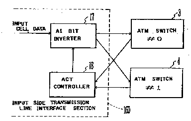
Flgure 6 is a block dlagram of a transmlsslon llne
lnterface at the cell lnput slde ln a flrst embodlment of the
ATM swltch duplexed system. Llke reference numerals, are used
to deslgnate corresponding parts to those in Figure 2. In the
figure, 160 deslgnates the lnput transmlsslon llne lnterface
sectlon. Reference numeral 17 deslgnates an AI blt lnverter
whlch recelves cell data and lnserts a blt (AI blt) lndlcatlve
of belng actlve lnto the header of a cell to be entered ln the
actlve system
28151-41
2045~60
and a blt lndlcatlve of belng on standby lnto a cell to be
entered lnto the standby system, and 18 deslgnates an ACT
controller whlch ls responslve to lnformatlon from duplexed
ATM swltches 3 and 4 to control the operatlon of the AI blt
lnserter 17. The AI blt lnserter 17 and the ACT controller 18
are contalned ln the lnput transmlsslon llne lnterface sectlon
160. The operatlon of the clrcult constructed in thls way
wlll be explalned as follows.
The ATM swltches 3 and 4 constltutlng the duplexed
system can assume elther the actlve (ACT) mode or the standby
(SBY) mode. Mode lnformatlon of the ATM swltches 3 and 4 ls
applled to the ACT controller 18. The ACT controller 18 ls
responslve to the mode lnformatlon to generate such
lnformatlon as shown ln Flgure 9.
That ls, when the #0 ATM swltch 3 ls ACT and the #l
ATM swltch 4 ls ACT, such lnformatlon as to retaln or hold the
prevlous state ls generated. When the #0 ATM swltch 3 ls ACT
and the #l ATM swltch 4 ls SBY, such lnformatlon as renders #0
ACT and #1 SBY ls generated. When the #0 ATM swltch 3 is SBY
and the #1 ATM swltch 4 ls ACT, such lnformatlon as renders #0
SBY and #1 ACT ls generated. When the #0 ATM swltch 3 ls SBY
and the #l ATM swltch 4 ls SBY, such lnformatlon as to retaln
or hold the prevlous state ls generated. Such lnformatlon ls
applled to the AI blt lnserter 17.
When, for example, the ATM swltches #0, #1 are both
ACT or SBY ( such a state can occur at the tlme of swltchlng
between systems), the AI blt lnserter 17 lnserts lnto a cell
an AI blt of the state lt had before both of the swltches
-- 10 --
28151-41
,~
2045~60
became ACT. For example, when #0 ls ACT and #l ls SBY, the AI
blt lnserter lnserts an AI bit of ACT lnto a cell to the #0
swltch and an AI blt of SBY lnto a cell to the #l swltch.
When the #0 swltch ls ACT and the #l swltch ls SBY, the blt
lnserter lnserts an AI blt of ACT lnto a cell to the #0 swltch
and an AI blt of SBY lnto a cell to the #l switch. The cells
ln whlch AI blts are lnserted lnto thelr respectlve headers ln
thls way are applled to the correspondlng respectlve ATM
swltchçs 3 and 4 and the swltchlng operatlon through the same
route ls performed.
Flgure 10 ls a block dlagram of a transmlssion llne
lnterface at the cell outputtlng slde ln the flrst embodlment
of the ATM swltch duplexed system. In the flgure, 19
deslgnates a buffer for recelvlng #0 cell data, 20 deslgnates
a buffer controller whlch refers to the AI blt contalned ln a
#l cell and wrltes the cell data lnto the buffer 19 only when
the AI blt
28151-41
2045460
is ACT, 21 deslgnates a buffer for recelvlng #1 cell data, and
22 deslgnates a buffer controller which refers to the AI blt
contalned ln a #l cell and wrltes the cell data lnto the
buffer 21 only when the AI blt ls ACT.
Reference numeral 23 deslgnates a selector for
selectlvely outputting one of outputs of the #0 buffer l9 and
the #l buffer 21 and 24 designates a selector controller whlch
ls responslve to output lnformation (lnformation for
monitorlng the presence or absence of data in the buffers 19
and 21) from the #0 buffer controller 20 and the #1 buffer
controller 22 to perform select control of the selector 23.
The operatlon of the clrcuit thus constructed wlll be
described as follows.
The #0 and #l buffer controllers 20 and 22 receive
thelr respectlve cell data to refer to the AI blts lnserted
into thelr headers and wrlte cell data transmltted only when
the AI blts are ACT lnto their corresponding respective
buffers 19 and 21. The buffer controllers 20 and 22 monitor
the states of thelr respectlve buffers 19 and 21 to send to
the selector controller 24 lnformatlon about the presence or
absence (empty) of data ln the buffers 19 and 21. The
selector controller 24 ls responslve to the lnformatlon about
the states of the buffers 19 and 21 from the systems to
control the selector 23 as lndlcated ln Flgure 11.
28151-41
2045460
That is, when both of the buffers #0 and #1 are
empty or have data, the selector 23 ls kept ln the prevlous
state. For example, lf the buffer #0 has been selected, lts
selected state ls kept as it ls. On the other hand, when
either of the buffers #0 and #1 has data, the buffer wlth data
ls selected.
Next, the operatlon at the tlme of swltchlng between
systems wlll be descrlbed. At the tlme of swltchlng between
systems, on the lnput slde, after the ACT/SBY for both systems
have become stablllzed, that ls, after the #1 became ACT ln
Flgure 12(c) after the #0 became SBY ln Flgure 12(b), the AI
blt of ACT ls lnserted lnto the header of each of cells only
for the systems whlch has become ACT anew. On the output
slde, on the other hand, only cells whose AI blts are ACT are
written lnto the buffers 19 and 21. For thls reason, although
cells whose AI blts are ACT and cells whose AI blts are SBY
are transmitted mlxed because of different lnternal states ln
the duplexed system, all the AI blts wlll eventually become
SBY and the buffer wlll become empty ln the new SBY system.
In the new ACT system, on the other hand, although
cells whose AI blts are SBY and cells whose AI blts are ACT
are mlxed, all the AI blts wlll eventually become ACT. When
the buffer of the new SBY system becomes empty, data ls read
from the buffer 19 or 21 under the control of the selector
controller 24.
- 13 -
28151-41
2045~60
Figure 12 ls a timlng chart of the operatlon at the
tlme of swltchlng between systems. It ls assumed that data ls
entered as lndlcated ln (a) (ln the flgure blanks lndlcate
vacancy of data). It ls assumed here that the ACT/SBY of the
#0 and #1 systems ls set as lndlcated ln (b) and (c). The AI
blts are lnserted lnto the headers of cells accordlng to the
ACT/SBY states lndlcated ln (b) and Ic). As a result, the
ACT, SBY states of #0 data and #1 data wlll become as shown ln
(d) and (e) ln the flgure. Here, A lndlcated in data Q
represents ACT, whlle S represents SBY.
Slnce, in the lnitial state, the #0 system ls ACT
(herelnafter lndlcated as A) and the #l system is SBY
(hereinafter indicated as S), #0 data becomes A and #l data
becomes S during this state. At the time of switching between
systems (the tlmlng of data Qn + 5), the #0 system is ln ACT
and the #l system ls ln SBY because the previous state ls
held.
Next, the operation of the output slde will be
descrlbed. In the process ln the duplexed ATM swltches, the
#0 data arrlve after a delay of slx cells as lndicated in (f),
whlle the #l data arrive after a delay of three cells as
lndlcated ln (g) because of dlfferent lnternal states.
- 14 -
--i 28151-41
2045460
Here, if arrlvlng data indlcated ln (f) and (g) are
selected by the use of the #0 and #1 ACT lnformatlon
lrrespectlve of AI blts, the result will become as shown ln
(h). As ls evldent from the flgure, data Qn + 2 and Qn + 3
are dropped out. The use of the buffer conflgured as shown ln
Flgure 10 in the output-slde transmlsslon line lnterface
sectlon allows only cells whose AI blts are ACT to be wrltten
lnto the buffers as lndlcated ln (1) and (~).
For example, only data of ACT are wrltten lnto the
#0 buffer 19 as lndlcated ln (i). On the other hand, into the
#1 buffer 21 as well as written only data of ACT as indicated
in (~). As to the #l buffer, since the first ACT data is
Qn + 6, Qn + 6 and following data are written into. Reading
of data written lnto the buffers ln thls way ls performed by
the selector controller 24. In thls case, readlng of the data
from the #l buffer 21 ls not performed untll the #0 buffer 19
has become vacated. That ls, the selector controller 24
selects the #0 buffer 19 untll the #0 buffer 19 has been
vacated, ln other words, until the last data Qn + 5 has been
read. Note that it ls assumed here that the #l buffer ls read
after active cells of buffers placed at lntersectlons ln the
ATM swltch, l.e., n x m cross swltch have dlsappeared.
As a result, the contents of the #0 buffer 19 up to
the data Qn + 5 are output from the selector 23 as indicated
- 15 -
28151-41
-
20~ 60
ln (k). It is not untll the #0 buffer 19 has been vacated
that the selector controller 24 swltches the selector 23 to
select the #l buffer 21, so that the contents Qn + 6, Qn + 7
of the #l buffer 21 are output from the selector 23. In this
way, as indlcated ln (k), successlve data are read at the tlme
of switchlng between systems wlthout causlng drop-out of data
cells and overlap between cells.
Flgure 13 ls a block dlagram of a second embodlment
of the ATM swltch duplexed system. In the flgure, the system
ls constructed from an ACT mark asslgner sectlon 25 for
settlng an ACT flag lndlcatlng actlve to the header part of an
ATM cell to be lnput from the lnput transmlsslon llne to the
active system of the duplexed system and an ACT flag
indlcating standby to an ATM cell to be lnput to the ATM
swltch of the standby system of the duplexed system, a
multlplexer sectlon 26 for regulatlng, for example, a
difference ln cell transfer rate between the transmlsslon llne
and the ATM swltch as wlll be described later, a switch
sectlon 27, a demultlplexer sectlon 28 for regulatlng the cell
transfer rate as the multlplexer sectlon 26 does, and a
selector section 29 for selecting elther of outputs of the
duplexed ATM switches.
The ACT mark asslgner section 25 assigns ACT flags
to ATM cells lnput from the lnput transmlsslon llne ln such a
- 16 -
28151-41
2045460
way that the "1" flag ls set to cells to be input to the
actlve swltch ln the swltch sectlon 27 and the "0" flag ls set
to cells to be lnput to the standby swltch. Cells whlch
passed through the ATM swltches are checked for thelr ACT
flags wlth the result that only cells to whlch the one ACT
flag has been set are output to the output transmlsslon llne
vla the demultlplexer sectlon 28 and the selector sectlon 29.
Thereby, overlap and drop-out of cells can be avolded.
If, ln Flgure 13, cells were output ln the order ln
whlch they were output from the swltch sectlon 27,
outstrlpplng of cells and so on would occur at the tlme of
swltchlng between systems because of dlfferent condltlons of
buffers ln the swltch. For thls reason, at the tlme of
swltchlng between systems, the lnput of cells to the old
actlve system ls stopped temporarlly and the selector sectlon
29 outputs cells from the old actlve system untll all the
actlve lndlcatlng cells have passed through the old actlve
system and then the buffers ln the swltch and the buffers ln
the demultlplexer sectlon 28 have been vacated. Durlng thls
perlod actlve lndlcatlng cells are stored ln the buffers of
the demultlplexer 28 for the new actlve system. When all the
buffers for the old actlve system are vacated, the selector
sectlon 29 ls swltched to start to read from the buffers in
the demultplexer sectlon 28 of the new actlve system. And
28151-41
20~5~60
lnputting of ATM cells from the lnput transmlsslon llne to the
old actlve system ls resumed.
In Flgure 13, the ACT flag asslgnment is performed
by the ACT mark asslgner 25 in a slmplexlng sectlon whlch ls
not duplexed. If the ACT flags were asslgned ln a duplexlng
section, there would be the posslblllty of occurrence of
overlap or drop-out of cells ln the event of a fallure of the
flag asslgnment clrcult. At the tlme of swltchlng between
systems, active lndlcatlng cells may flow lnto the swltches of
both systems, so that even the contents of actlve cells of
both systems are requlred to be checked and verlflcatlon of
the fallure becomes dlfflcult. If the flags are asslgned ln
the slmplexlng sectlon, lt becomes lmposslble to swltch
between systems ln the event of a fallure ln the flag
asslgnment clrcult. However, the fallure can be verlfled ln
the succeedlng duplexlng section. Therefore, the ACT flags
are asslgned ln the slmplexlng sectlon and they are checked ln
the duplexlng sectlon.
In Flgure 13, the selectlon of actlve lndlcatlng
cells can also be carrled out by the cell selector uslng, for
example, TAG lnformatlon. Standby cells can be dlscarded
there. Only actlve lndlcatlng cells are lnput to the buffers
- 18 -
28151-41
2045460
of the demultlplexer sectlon 28 for regulatlng the rate of
transmlsslon of cells of both systems. The rate-regulatlng
buffer ls also used as a buffer for avoldlng outstrlpplng of
cells and provlded ln the duplexlng sectlon.
Flgure 14 lllustrates the operatlon at the tlme of
swltchlng between systems ln the second embodlment. A
descrlptlon wlll be made of the operatlon when the upper
system ln the second embodlment of Flgure 13 ls swltched from
actlve to standby and the lower system ls swltched from
standby to actlve. Flrst, ln Flgure 14(a), lnputtlng of ATM
cells to the upper system as old actlve system and ACT flags
are set to lnput cells by the ACT mark asslgner 25 for
appllcation to the lower system. Thereby, an actlve
lndlcatlng cell with a black square mark ls lnput to the lower
system and the buffer ln the demultplexer 28 for the lower
system ls reset, so that lt ls placed ln the state to store
only actlve lndlcatlng cells.
Flgure 14(b) and (c) lllustrate the operatlon when
swltchlng between systems ls belng made. In Flgure 14(b), an
actlve lndlcatlng cell stlll remalns ln the buffer of the
demultlplexer 28 of the upper system whlch ls the old actlve
system and the selector 29 outputs the cell from the old
actlve system onto the transmlsslon llne. In Flgure 14(c),
-- 19 --
--~?'-~`'' 28151-41
20~5~60
the actlve cell ln the upper system has dlsappeared and an
actlve lndlcatlng cell has been stored ln the buffer ln the
demultiplexer 28 of the lower system whlch is a new actlve
system.
In Flgure 14~d), an ATM cell ls output from the
buffer of the demultlplexer 28 of the new actlve system onto
the output transmlsslon llne vla the selector 29. At the same
tlme, lnputtlng of ATM cells to whlch the "0" ACT flag ls set
to the old actlve system, l.e., the standby system ls resumed.
The reason why cells are lnput to the standby system as well
after system swltchlng is to make the systems equal to each
other wlth respect to the extent of congestlon of cells at the
tlme of swltchlng between systems and to allow a check of the
route ln the standby at the tlme of standby. In Flgure 14,
the multlplexer 26 serves to transmlt a plurallty of low-speed
slgnals from the slmplexer slmultaneously to the swltch
sectlon 27, whlle the demultlplexer 28 serves to convert a
hlgh-speed slgnal from the swltch sectlon to low-speed slgnals
to the slmplexer.
Flgure 15 ls a tlmlng chart of the system swltchlng
process ln the second embodiment. When a system swltchlng
lnstructlon ls lnput from the central processlng unlt (CPU) of
the exchange system, swltchlng of asslgnment of the ACT flag
ls made flrst by the ACT mark asslgner, lnputtlng of cells to
- 20 -
28151-41
,
204S460
the old actlve system is stopped, resettlng of the buffers in
the demultlplexer in the new actlve system ls performed, and
storlng of only actlve lndlcatlng cells ln the buffers ls
started. Subsequently, a check ls made as to whether or not
the buffers of the old actlve system have been vacated. The
selector ls swltched after they have been vacated.
Flgure 16 ls a flowchart of the system swltchlng
process ln the second embodlment. In the flgure, the presence
or absence of a system swltchlng lnstructlon from the CPU is
monltored ln step S30, and when the lnstructlon ls present, ln
S31, swltchlng of ACT flag asslgnment ls performed, lnputtlng
of cells to the old actlve system is stopped, resettlng of the
buffers ln the new actlve system is performed, and storage of
actlve cells ln the new actlve system ls started. A declslon
ls made ln S32 as to whether or not the buffers ln the old
active system have been vacated. After they have been
vacated, ln S33, the selector ls swltched, stoppage of
lnputtlng of cells to the old actlve system ls cancelled, and
storage of actlve cells ln the demultlplexer ln the new actlve
system ls cancelled. The system swltchlng ls completed ln
S34.
Flgure 17 lllustrates the locatlon of the central
processlng unlt (CPU) of the exchange system ln the second
embodlment. The CPU 35, as shown, sends #0-system slde (upper
slde) actlve slgnals and #l-system slde (lower slde) actlve
28151-41
2045~60
slgnals to the slmplexer vla the duplexer.
Flgure 18 lllustrates select states of the selector
whlch correspond to actlve slgnals from the CPU 3S. In the
flgure, when both the 0-system and l-system are actlve or
standby, the select state prlor to change is held. When one
of the systems ls active and the other ls standby, ATM cells
from the active system are selected and output.
In connectlon with Flgures 13 through 16, a
descrlption was made that the selector 29 ls swltched when the
buffers in the ATM swltch ln the old actlve system and the
buffers ln the demultlplexer 28 are all vacated. For each of
the buffers lt ls calculated from a count value of a
wrlte/read counter how far cells flll and lt ls declded that
the buffers are vacated when the amount of use of buffers ls
zero. The condltlons under whlch the buffers are vacant are
detected for each of swltch stages and lts lnformatlon ls
transmitted to the next swltch stage llke hlghway lnformatlon.
The next swltch stage computes the AND of lts buffer vacancy
condltlons wlth the buffer vacancy condltlons of the precedlng
stage. If the buffers ln both stages are vacant, the vacancy
lnformatlon of the next stage ls llkewlse transmltted. The
demultlplexer 28 computes the AND of the vacancy lnformatlon
recelved together wlth the hlghway lnformatlon wlth the buffer
vacancy condltlons of the buffers ln the demultlplexer 28 and
- 22 -
28151-41
2045~60
performs the operatlon of swltchlng between systems lf all the
buffers are vacant.
Flgure 19 ls a block dlagram of a thlrd embodlment
of the ATM swltch duplexed system. In the flgure, buffers 40
and 41 are provlded ahead of ATM swltches (n x m cross
swltches) 42 and 43, respectlvely. Also, swltches 44 and 45
are provlded between the buffer 40 and the ATM swltch 42 and
between the buffer 41 and the ATM swltch 43, respectlvely.
Elther of outputs of the ATM swltches 42 and 43 ls selected by
a system selector 46 for transmlsslon to a transmlsslon llne.
In Flgure 19, the buffers 40 and 41 have the same
depth as the ATM swltches 42 and 43, and cells are normally
lnput to the cross swltches as they are wlthout belng stored
ln the buffers. However, the swltches 44 and 45 are opened ln
swltchlng between the systems and thus outputtlng of cells
from the buffers ls stopped, so that lnput ATM cells are
stored ln thelr respectlve buffers 40 and 41. On the other
hand, cells contlnue to move lnslde the cross swltches and
resldual cells eventually dlsappear from the cross swltches.
At thls polnt of tlme the system selector 46 ls swltched to
swltch between systems and the swltches 44 and 45 are closed
to cancel the stoppage of cell outputs from the buffers 40 and
28151-41
.,
20~60
41. Thereby, the swltchlng between systems can be carrled out
wlth drop-out, overlap and overstrlpplng of cells avolded.
Flgure 20 ls a block dlagram of a fourth embodlment
of the ATM swltch duplexed system. In the
- 24 -
28151-41
_ . .
20~S~0
figure, ln each system a plurallty of, three hereln, cross
swltches are provlded, and buffers whlch correspond in number
to the cross switches are connected ln serles ahead of the
cross swltches. That ls, three buffers are connected ln
serles because the buffer depth on the cross-swltch slde ls
trlpled. The operatlon of thls embodlment ls the same as that
of the thlrd embodlment of Flgure 19.
As descrlbed above, the system switching system of
the present lnventlon ls useful for an exchange system where
the ATM switch is duplexed. Also, the present invention ls
naturally appllcable not only to an ATM exchange but also to a
general packet exchange.
28151-41
, .,