Language selection

Search

Patent 2045489 Summary

Third-party information liability

Some of the information on this Web page has been provided by external sources. The Government of Canada is not responsible for the accuracy, reliability or currency of the information supplied by external sources. Users wishing to rely upon this information should consult directly with the source of the information. Content provided by external sources is not subject to official languages, privacy and accessibility requirements.

Claims and Abstract availability

Any discrepancies in the text and image of the Claims and Abstract are due to differing posting times. Text of the Claims and Abstract are posted:

  • At the time the application is open to public inspection;
  • At the time of issue of the patent (grant).
(12) Patent: (11) CA 2045489
(54) English Title: OPTICAL FIBER COUPLER
(54) French Title: COUPLEUR DE FIBRES OPTIQUES
Status: Expired and beyond the Period of Reversal
Bibliographic Data
(51) International Patent Classification (IPC):
  • G02B 06/40 (2006.01)
  • G02B 06/36 (2006.01)
  • G02B 06/42 (2006.01)
(72) Inventors :
  • NEWELL, EDWIN RASBERRY (United States of America)
(73) Owners :
  • SQUARE D COMPANY
(71) Applicants :
  • SQUARE D COMPANY (United States of America)
(74) Agent: SMART & BIGGAR LP
(74) Associate agent:
(45) Issued: 1998-12-29
(86) PCT Filing Date: 1990-11-05
(87) Open to Public Inspection: 1991-05-10
Examination requested: 1997-11-04
Availability of licence: N/A
Dedicated to the Public: N/A
(25) Language of filing: English

Patent Cooperation Treaty (PCT): Yes
(86) PCT Filing Number: PCT/US1990/006380
(87) International Publication Number: US1990006380
(85) National Entry: 1991-07-02

(30) Application Priority Data:
Application No. Country/Territory Date
433,941 (United States of America) 1989-11-09

Abstracts

English Abstract


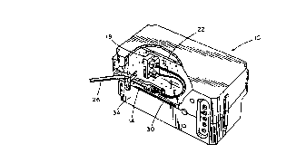
An optical fiber coupler including an optical fiber
having an end, and an electronic light pulse communication
assembly comprising an assembly housing, an electronic light
pulse communication device fixed within the assembly housing,
and a lens mounted on the assembly housing and in light pulse
communication with the electronic light pulse communication
device. The optical fiber coupler also includes a coupler
housing having an inlet well, an assembly well separated from
the inlet well by a coupler housing well and having the
assembly fixedly received therein, and a fiber passage which
extends between the inlet well and the assembly well and which
snugly receives the fiber so that the fiber end is adjacent
the assembly lens. The coupler housing further includes epoxy
in the inlet well so that the fiber is secured to the coupler
housing, and index matching gel surrounding the optical fiber
end to assembly lens junction so that substantially all of the
light passing between the assembly lens and the fiber does not
escape from the optical fiber end to assembly lens junction.


Claims

Note: Claims are shown in the official language in which they were submitted.


The embodiments of the invention in which an exclusive property
or privilege is claimed are defined as follows.
1. An optical fiber coupler comprising
an optical fiber having an end,
an electronic light pulse communication assembly comprising
an assembly housing,
an electronic light pulse communication device fixed within
said assembly housing, and
a lens mounted on said assembly housing and in light pulse
communication with said electronic light pulse communication
device, and
a coupler housing having
an inlet well,
an assembly well separated from said inlet well by a
coupler housing wall and having said assembly fixedly received
therein, and
a fiber passage which extends between said inlet well and
said assembly well and which snugly receives said fiber so that
said fiber end is adjacent said assembly lens,
said coupler housing further including
epoxy in said inlet well so that said fiber is secured to
said coupler housing, and
index matching gel surrounding said optical fiber end to
assembly lens junction so that substantially all of the light
passing between said assembly lens and said fiber does not
escape from said optical fiber end to assembly lens junction.

2. An optical fiber coupler in accordance with Claim 1
wherein said electronic light pulse communication device is an
emitter.
3. An optical fiber coupler in accordance with Claim 1
wherein said electronic light pulse communication device is an
detector.

11
4. A coupler for connecting a plurality of fibers to a
printed circuit board, the coupler including
a coupler housing adapted to be connected to the printed
circuit board, said housing having
a plurality of spaced-apart inlet wells,
a plurality of spaced-apart assembly wells separated from
said inlet wells by a coupler housing wall,
a plurality of fiber passages, each of which snugly
receives one of the plurality of fibers and which extends
between a separate one of said inlet wells and a separate one of
said assembly wells,
a detector assembly comprising
a detector assembly housing,
a detector fixed within said detector assembly housing and
electrically connected to the circuit board, and
a lens mounted on said detector assembly housing and in
light pulse communication with said detector, said detector
assembly being fixedly received in one of said assembly wells so
that said detector assembly lens is adjacent the fiber in said
assembly well's fiber passage, and
an emitter assembly including
an emitter assembly housing, an emitter fixed within said
emitter assembly housing and electrically connected to the
circuit board, and
a lens mounted on said emitter assembly housing and in
light pulse communication with said emitter, said emitter
assembly being fixedly received in another of said assembly

12
wells so that said emitter assembly lens is adjacent the fiber
in said assembly well's fiber passage.
5. A coupler in accordance with claim 4 wherein
each of said plurality of assembly wells has a plurality
of crushable nibs for fixedly securing each of said detector
assembly and said emitter assembly in its respective assembly
wells.

Description

Note: Descriptions are shown in the official language in which they were submitted.


2 ~ 9
OPTICAI F1BFR COUPI FF~
FIELD OF THE INVENTION
This invention relates to connections and couplers for
connecting optical fibers to other optical fibers and to printed
circuit boards.
SUMMARY OF THF ~NVENTION
This invention comprises an optical fiber coupler including
an optical fiber having an end, and an electronic light pulse
c ication assembly comprising an assembly housing, an :~
10 electronic light pulse c: lication device fixed within the -
assembly housing, and a lens mounted OD the assembly housing and
in light pulse c~ -ication with the electronic light pulse
c~ ication device.
The optical fiber coupler also includes a coupler housing
having an inlet well, an assembly well separated from the inlet
well by a coupler housing wall and having the assembly fixedly
received therein, and a fiber passage which extends between the
inlet well and the assembly well and which snugly receive~ the
fiber so that the fiber end is adjacent the assembly lens.
~he coupler housing further includes epoxy in the inlet
well so that the fiber is secured to the coupler housing, and
index matching gel surrounding the optical fiber end to assembly
lens junction so that substantially all of the light passing
; between the assembly lens and the fiber does not escape from the
optical fiber end to assembly lens junction.
~ ; . , . .:
.

2 ~ 9
One Gf the features of the invention is the provision of an
efficient and secure optical fibers to printed circuit board
coupler. This coupler insures a good fibers to printed circuit
board connection with substantially all of the light passing
between the fibers and the electronic communication device.
Prior art couplers have not been known to ~e able to both use an
epoxy to fix a fiber end in place while at the same time being
able to use an index gel at a fiber end to lens junction to help
insure all light passes between the fiber end and the lens.
Other features and advantaqes of the invention will become
apparent to those skilled in the art upon review of the
following detailed description, claims and drawings.
BRIFF DF~C~ ON OF THE D~AWINGS
Figure 1 is a perspective view, partially broken away, of a
fiber optical transceiver which embodies various of the features
of the invention.
Figure 2 is a side view of a coupler for connecting a
plurality of fibers to a printed circuit board which embodies
various of ~he features of the invention.
Figure 3 is an end view of the coupler illustrated in
Figure 2.
Figure 4 is a cross sectional view of the coupler
illustrated in Figure 2 taken along the line 9-~ in Figure 3.
Figure 5 is a cross sectional view of the coupler
illustrated in Figure 2 taken along the line 5-5 in Figure 2.
~ . .. .
:'-
. -
'

Figure 6 is an exploded view illustrating the fiber end to
lens junction in the coupler illustrated in Figure 9.
Figure 7 is a side view of a coupler housing used to
construct the coupler illustrated in Figure 2. The coupler
S housing is viewed from along the line 7-7 in Figure 5.
Figure 8 is a top view of the fiber to fiber connection
which is illustrated in Figure 1 and which embodies various of
the features of the invention. The connection includes a
coupler housing and is shown with a first fiber end only
partially inserted and with a shuttle in its second position.
Figure 9 is a cross sectional view of the shuttle and the
coupler housing taken along the line 9-9 in Figure 8.
~ igure 10 is top view of the fiber to fiber connection with
the first fiber end fully inserted and with the shuttle in its
lS first fiber connecting position.
Figure 11 is a cross sectional view of a clamp used to
grasp the first fiber end and fix it to the coupler housing
taken along the line 11-11 in Figure 10.
Before one embodiment of the invention is explained in
detail, it is to be understood that the invention is not limited
in its application to the details of construction and the
arrangement of c~ ents set forth in the following description
or illustrated in the drawings. The invention is capable of
other embodiments and if being practiced or being carried out in
various ways. Also, it is to be understood that the phraseology
and terminology used herein is for the purpose of description
and should not be regarded as limiting.
' : , ''' : '' .-,,; : ' -

,~,3 ~
DETAILED DESCRIPTION OF THE PREFERRED EMBODIMENT
OF THE INVENTION
Illustrated in the drawings is 2 fiber optic transceiver 10
for transmitting and receiving opticzl pulses. The transceiver
S 10 includes a fiber to fiber connection 14, an optical fiber
coupler 18, and a conventional transceiver processing and
indicating means including a printed circuit board 22.
More particularly, the fiber to fiber connection 14
includes a first optical fiber end 26, a second optical fiber
end 30, and a connector housing 34. The connector housing 34
has a connection chamber 38 (see Fig. 8), a first fiber inlet
passage 42 which - nicates with the connection chamber 38 and
which snugly but slidably receives the first fiber end 26, and a
second fiber inlet passage 46 which c~ icates with the
lS connection chamber 38 and which slidably receives the second
fiber end 30. The second fiber inlet passage 46 enters the
connection chamber 38 on a side opposite from the first fiber
inlet passage 42.
The fiber to fiber connection 14 further includes a shuttle
S0 slidably received within the connection chamber 38 and
movable between a first fiber connecting position (see Fig. 10)
and a second position ~see Fig. 8). The shuttle 50 has a fiber
receiving end 54, and a connection end 58 housing the second
fiber end 30. The connection end 58 is snugly but slidably
received within the first fiber inlet passage 42 so that the
second fiber end 30 faces the first fiber end 26. More
particularly, there are a plurality of second fiber ends 30
. : . ,
- , '- ' '
.: . . : ' .. ~

slidably received in the second fiber inlet passage 46 and each
of the second fiber ends 30 is housed by the shuttle connection
end 58 so that each of the second fiber ends 30 face the first
fiber 26 and so that the first fiber end 26 is held in
5 compression against all of the second fiber ends 30. In the
preferred embodiment, the second fiber ends 30 are fixed in the
connection end 58 with epoxy, and the connection end 58 is
ground down to where each of the fiber ends 30 are flush with
the connection end 58.
The fiber to fiber connection 14 further includes means
for biasing the shuttle 50 toward the first fiber inlet passage
42 from the first fiber connecting position (Fig. 10) to the
second position (Fig. 8). More particularly, the shuttle S0 has
an enlarged middle 62 between the fiber receiving end 54 and the
15 connection end 58, and the biasing means comprises a compression
spring 66 concentric about the fiber receiving end 54, the
spring 66 having one end bearing against the connector housing
34 and another end bearinq against the shuttle middle 62.
The fiber to fiber connection 14 further includes means 70
20 for fixing the first fiber end 26 within the first fiber inlet
passage 42 with the first fiber end 26 adjacent the shuttle
connection end 58 and with the shuttle 50 held by the first
fiber end 26 in the first fiber connecting position (Fig. 10) so
that the first fiber end 26 is held in compression against the
25 second fiber end 30. More particularly, the means 70 for fixing
the first fiber end 26 within the first fiber inlet passage 42
comprises a slot 74 in the connector housing 34 and extending
- . .. , .: . ,: ': .. . -
-: , . . ,. :, .. .
. ~
. . . ~ ~ . : -
.
': :, ....

across the first fiber inlet passage 42, and a clamp ?8 received
within the slot 79 and grasping the first fiber end 26.
The first fiber inlet passage 42 is curved so that the
first fiber end 26 is biased by its own resiliency against a
wall of the first fiber inlet passage 42 to effect a more exact
registry between the first fiber end 26 and the second fiber end
30.
The connector housinq 34 includes a first piece having a
first piece surface 82 (see Fig. 9) and a second piece having a
10 second piece surface 86 abutting the first piece surface 82.
The first fiber inlet passage 42, the connection chamber 38, the
second fiber inlet passage 46, and the slot 74 are defined by
the first and the second piece surfaces.
As illustrated in Figs. 2 t}~rough 7, the fibers to printed
lS circuit board coupler 18 includes a coupler housing 90 (see Fig.
5) adapted to be connected to the printed circuit board 22. The
coupler housing 90 has two spaced-apart inlet wells 99 (see Fig.
4), two spaced-apart assembly wells 9B separated from the inlet
wells 94 by a coupler housing wall 102, and two fiber passages
20 106. Each of the fiber passages 106 snugly receives at least
one of the plurality of fibers 30 and extends between a separate
one of the inlet wells 94 and a separate one of the assembly
wells 98. More particularly, two fibers 30 are received in one
assembly well 98 and one fiber is received in the other assembly
25 well 98.
The coupler 18 further includes a detector assembly 110
comprising a detector assembly housing 114, a detector 118 fixed
.. . . .
,
,:

2 $ ~t~ ~9
within the detector assembly housing 114 and electrically
connected (see Fig. S) to the printed circuit board 22, and a
detector assembly lens 122 mounted on the assembly housing 114
and in light pulse communication with the detector 118, the
S detector assembly 110 being fixedly received in one of the
assembly wells 98 so that the detector assembly lens 122 is
adjacent the fiber in the assembly well's fiber passage.
The coupler 18 further includes an emitter assembly 126
including an emitter assembly housing 130, an emitter 134 fixed
within the emitter assembly housing 130 and electrically
connected to the printed circuit board 22, and an emitter
assembly lens 138 mounted on the emitter assembly housing 130
and in light pulse c~ -;cation with the emitter 134, the
emitter assembly 126 being fixedly received in another of the
assembly wells 98 so that the emitter assembly lens 138 is
adjacent the fiber in the assembly well's fiber passage. More
particularly, as illustrated in Figures 5 and 7, each assembly
well 98 has a plurality of crushable nibs 150 for fixedly
securing each of the detector assembly 110 and the emitter
assembly 126 in its respective assembly well 98.
The coupler housinq 90 further includes epoxy 142 in each
fiber inlet well 94 so that the fiber is secured to the coupler
housing 90, and index mztching gel 146 surrounding each optical
fiber end tc assembly l- junction so that substantially all of
the light p_3sing betwe~ ~he assembly lens and the fiber does
not escape from the optical fiber end to assembly lens junction.
.
' ,,, :' ~ ,

2 $ ~
~he housing wall 102 keeps the indexing gel 196 from mixing with
the epoxy 192.
Various features of the invention are set forth in the
following claims.
- . ~ . : . , :
. ~ . .
:

Representative Drawing
A single figure which represents the drawing illustrating the invention.
Administrative Status

2024-08-01:As part of the Next Generation Patents (NGP) transition, the Canadian Patents Database (CPD) now contains a more detailed Event History, which replicates the Event Log of our new back-office solution.

Please note that "Inactive:" events refers to events no longer in use in our new back-office solution.

For a clearer understanding of the status of the application/patent presented on this page, the site Disclaimer , as well as the definitions for Patent , Event History , Maintenance Fee  and Payment History  should be consulted.

Event History

Description Date
Inactive: IPC from MCD 2006-03-11
Time Limit for Reversal Expired 2004-11-05
Letter Sent 2003-11-05
Grant by Issuance 1998-12-29
Inactive: RFE acknowledged - Prior art enquiry 1998-09-09
Inactive: Final fee received 1998-07-09
Pre-grant 1998-07-09
Inactive: Correspondence - Prosecution 1998-07-06
Inactive: Correspondence - Prosecution 1998-05-04
Notice of Allowance is Issued 1998-02-12
Letter Sent 1998-02-12
Inactive: Application prosecuted on TS as of Log entry date 1998-02-10
Inactive: Status info is complete as of Log entry date 1998-02-10
Inactive: IPC assigned 1998-01-02
Inactive: IPC removed 1998-01-02
Inactive: First IPC assigned 1998-01-02
Inactive: Approved for allowance (AFA) 1998-01-02
Inactive: IPC assigned 1998-01-02
Inactive: IPC removed 1998-01-02
Request for Examination Requirements Determined Compliant 1997-11-04
All Requirements for Examination Determined Compliant 1997-11-04
Application Published (Open to Public Inspection) 1991-05-10

Abandonment History

There is no abandonment history.

Maintenance Fee

The last payment was received on 1998-10-05

Note : If the full payment has not been received on or before the date indicated, a further fee may be required which may be one of the following

  • the reinstatement fee;
  • the late payment fee; or
  • additional fee to reverse deemed expiry.

Patent fees are adjusted on the 1st of January every year. The amounts above are the current amounts if received by December 31 of the current year.
Please refer to the CIPO Patent Fees web page to see all current fee amounts.

Fee History

Fee Type Anniversary Year Due Date Paid Date
MF (application, 7th anniv.) - standard 07 1997-11-05 1997-10-01
Request for examination - standard 1997-11-04
Final fee - standard 1998-07-09
MF (application, 8th anniv.) - standard 08 1998-11-05 1998-10-05
MF (patent, 9th anniv.) - standard 1999-11-05 1999-10-04
MF (patent, 10th anniv.) - standard 2000-11-06 2000-10-03
MF (patent, 11th anniv.) - standard 2001-11-05 2001-10-05
MF (patent, 12th anniv.) - standard 2002-11-05 2002-10-02
Owners on Record

Note: Records showing the ownership history in alphabetical order.

Current Owners on Record
SQUARE D COMPANY
Past Owners on Record
EDWIN RASBERRY NEWELL
Past Owners that do not appear in the "Owners on Record" listing will appear in other documentation within the application.
Documents

To view selected files, please enter reCAPTCHA code :


To view images, click a link in the Document Description column. To download the documents, select one or more checkboxes in the first column and then click the "Download Selected in PDF format (Zip Archive)" or the "Download Selected as Single PDF" button.

List of published and non-published patent-specific documents on the CPD .

If you have any difficulty accessing content, you can call the Client Service Centre at 1-866-997-1936 or send them an e-mail at CIPO Client Service Centre.


Document
Description 
Date
(yyyy-mm-dd) 
Number of pages   Size of Image (KB) 
Drawings 1994-03-30 2 72
Claims 1994-03-30 4 77
Abstract 1994-03-30 1 30
Description 1994-03-30 8 246
Representative drawing 1998-12-17 1 9
Reminder - Request for Examination 1997-07-04 1 117
Commissioner's Notice - Application Found Allowable 1998-02-11 1 165
Acknowledgement of Request for Examination 1998-09-08 1 177
Maintenance Fee Notice 2003-12-30 1 174
Correspondence 1998-07-08 1 38
Fees 1996-10-01 1 76
Fees 1995-10-09 1 47
Fees 1994-10-11 1 59
Fees 1993-10-27 1 44
Fees 1992-09-29 1 38
Prosecution correspondence 1997-11-03 1 71
International preliminary examination report 1991-07-01 17 548