Note: Descriptions are shown in the official language in which they were submitted.
YO9-90-084 1 20~5944
FIELD OF 1~ INVENTION
This invention relates to an optical system having a flat
image field. More particularly, this invention relates to
an optical system having an input subsystem which has a
curved image field which is the input object to a second
subsystem, the output of which is a flat image field,
wherein the first subsystem is designed to compensate for
the field curvature of the second subsystem to result in
the flat image field. Most particularly, this invention
relates to an optical system wherein the input subsystem
is a lX system and the output subsystem is an NX system.
Most particularly, this invention relates to a
microelectronic lithographic lens for projecting a
substantially flat and substantially aberration free
image of a flat mask onto a flat semiconductor chip or
semiconductor chip packaging substrate.
BACKGROUND OF T~E INVENTION
In the fabrication of mircoelectronic components,
optical systems are used to project the image of a mask
onto a substrate which is typically a resist covered
semiconductor chip or a resist covered semiconductor chip
packaging substrate. Also, these optical systems can be
used to directly ablate the image of the mask onto a
substrate.
The image field of an optical system is generally curved.
The degree of curvature is determined by the Petzval sum.
To increase the throughput through lithographic tools, it
is desirable to be able to project a large object field
so that fewer exposures are re~uired to form patterns on
a microelectronic substrate. If a large object field
were to be used with com;nonly available high resolution
optical systems, the projected image will not be in good
focus only over a limited image field since
YO9-90-084 2 204~944
microelectronic substrates, such as semiconductor chips
and semiconductor chip packaging substrates are planar
with increased resolution or numerical aperture the
correction of the Petzval sum becomes more and more
difficult, are generally curved.
One solution to this problem is to use a curved substrate
which has a curvature corresponding to the field
curvature of the optical system. This is a not a
realistic solution for fabrication of microelectronic
components, since these components are planar.
Alternatively, a mask having a curvature which is the
negative of the curvature of the optical system can be
used to result in an output image field which is
substantially flat. This solution is also not realistic
since the creation of a curved mask would be costly and
require special tooling to fabricate.
It is an object of the present invention to provide an
optical system where a substantially flat and
substantially aberration free image field is projected
onto a substantially flat planar surface.
In accordance with the present invention, an optical
system having the desired reduction ratio lX for
projecting a reduced image of a mask is provided. For
this optical system, preferably a lX projection optical
subsystem is provided which projects an image of the
substantially flat mask, wherein the image has the
opposite curvature of the reduction NX subsystem and
thereby the image field of the reduction subsystem is
substantially flat.
U.S. Patent 4,812,028 to Matsumoto described a reflection
type reduction projection optical system for optical
lithography. For the Matsumoto system consisting of a
plurality of monocentric reflecting and refracting
surfaces and at least one aplanatic refracting surfaces.
The Petzval sum of all the aplanatic refracting surfaces
together and of all the remaining reflecting and
Y09-90-084 3 20~5944
refracting surfaces is corrected independently of each
other. In contradistinction, the Petzval sum according to
the present invention, is corrected by compensation of
the field curvature of the input subsystem with that of
the output subsystem resulting in a field compensated
design. Also, the input and the output subsystems are
essentially separately corrected for the odd aberrations,
such as coma and distortion. But the even aberrations,
such as spherical aberration, astigmatism and field
curvature are substantially corrected by compensation
between the subsystems.
In the Matsumoto system, all refracting and reflecting
surfaces except the aplanatic surface operate in
substantially the lX monocentric mode which is not true
in the system of the present invention. Both the systems
of the present invention and Matsumoto s system have an
intermediate image. The systems of the present invention
present a curved intermediate image preferably formed by
a lX input subsystem to serve as a curved input to an
output NX subsystem. This approach reduces the burden of
field correction in the refractor by presenting to the
refractor a compensatory curved field.
It is another object of the present invention to provide
an optical system having a flat image field wherein the
optical system has a lX subsystem which provides a curved
image which is the object of a second NX subsystem. The
output of the combined system is a substantially
aberration free and flat image field with very high
resolution.
It is another object of the present invention to
substantially correct for odd aberrations separately in
each subsystem.
It is another object of the present invention to
substantially correct for even aberrations by
compensating the even aberrations of one subsystem with
even aberrations in the other subsystem.
2045944
YO9-90-084 4
These and other objects, features and advantages of the
present invention will be readily apparent to those of
skill in the art from the following specification and the
appended drawings.
SUMMARY OF T~E INVENTION
In its broadest aspect the present invention is an
optical system having a substantially flat object field
and a substantially flat image field.
In more particular aspect of the present invention, one
optical subsystem compensates for the field curvature of
a second optical subsystem to form the substantially flat
image field.
In another more particular aspect of the present
invention, one optical subsystem provides a focused image
of an object on an image surface which has a curvature
that is substantially the opposite of the field curvature
of the second optical subsystem, so that the output of
the second optical subsystem is a substantially flat
image field.
In another more particular aspect of the present
invention, each subsystem is separately corrected for the
odd aberrations, such as coma and distortion.
In another more particular aspect of the present
invention, the even aberrations of the subsystems, such
as spherical aberration, astigmatism and field curvature
are compensated by each subsystem.
In another more particular aspect of the present
invention, one of the optical subsystems is a lX input
optical system and the other optical subsystem is an NX
output optical subsystem.
204594~
YO9-90-084 5
In another more particular aspect of the present
invention, the input optical subsystem is a catadioptric
subsystem and the output optical subsystem is a dioptric
subsystem.
In another more particular aspect of the present
invention, between the input optical subsystem and the
output optical subsystems there is an air-spaced lens
group which does reimaging of the primary stop.
In another more particular aspect of the present
invention, the air-spaced lens which is used for
reimaging the primary stop into the dioptric system has
the effect of providing image space telecentricity.
In another more particular aspect of the present
invention, one or more fold mirrors can be used to make
the system more compact.
BRIEF DESCRIPTION OF 1~ DRAWINGS
ig. 1.1 is a schematic representation of a full field
image.
ig. 1.2 is a schematic representation of a ring field
image.
ig. 2 is a schematic diagram of an optical system
according to the present invention.
ig. 3 is a cross-sectional view of the optical
elements in a specific embodiment of the
present invention.
ig. 4 is an expanded view of the catadioptric lX
system of Fig. 3.
ig. 5 shows an expanded view of two final optical
YO9-90-084 6 20459~4
components of the NX reduction subsystem of the
embodiment of Fig. 3.
ig. 6 shows how the beam splitting cube of the
catadioptric lX system of Fig. 4 is used to
image a mask.
ig. 7 shows an alternate embodiment to the
catadioptric lX system of Fig. 4, wherein a
reflecting prism combination is used to split
the field in order to generate an off axis
image field, such as a scanning ring or a slot
image field.
ig. 8 is a schematic of the optical system of Fig. 3
with full aperture rays from the object to the
image.
ig. 9 shows the embodiment of Fig. 7 without the
reflecting prism combination.
ETAILED DESCRIPTION OF THE PREFERRED EMBODIMENT
Fig. 1.1 and 1.2 show a comparison of the image field
output of a ring field system as compared to a full field
system. The shaded area 2 in Fig. 1.1 corresponds to a
circular image field of a full field system having axis
6. The image field of a full field system is not limited
to a circular field but it can have any geometrical shape
within the circular field. The shaded area 4 in Fig. 1.2
corresponds to an image field of a ring field system
having axis 8. For the ring field system to achieve a
useful image area equal in size to the full field system
and without scanning, the ring field image size will have
to be substantially larger. Therefore, for a non-scanning
ring field system to achieve the same useful image area
as the full field system, the optics of the ring field
system become substantially larger.
YO9-90-084 7 20459~4
The most practical use of the system described in U.S.
patent 4,812,028 to Mastsumoto is as a ring field type
system as is evident from location of the object O and
the image I in Fig 1. of Matsumoto. For the Matsumoto
system to achieve a useful image area comparable to that
of the full field system of the present invention, the
optical system of Matsumoto as shown in Matsumoto Fig. 1
must become substantially larger. Moreover, the
intermediate image I of Fig. 1 of Matsumoto appears to be
a flat image, which is the object, O of subsystem S2 of
the Matsumoto system of Fig. 1. Moreover, in the
Matsumoto system of Fig. 1 the input object O is
substantially in the same location as the output image
I . The optical system of Fig. 1 of Matsumoto is
therefore of limited utility as a reduction
photolithographic lens. To achieve a more practical
useful system wherein the input object O and the output
image I are not substantially in the same location
Matsumoto introduces substantial additional complexity,
shown, for example, in Fig. 6 and Fig. 7 of Matsumoto.
Furthermore, mirror M2 of Fig. 1 of Matsumoto is an
obstruction, for field point on axis, which prevents the
systems of Matsumoto from being used in the on-axis mode,
and therefore prevents these systems from achieving a
high numerical aperture.
The systems according to the present invention compensate
for the Petzval sum between subsystems, which makes the
correction of chromatic aberration less problematic,
particularly when an excimer laser is used for
illumination.
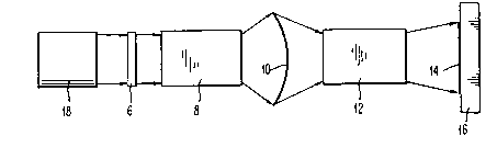
Fig. 2 is a schematic representation of an optical
subsystem according to the present invention. Object 6
is imaged through an optical subsystem 8 which projects a
real curved image 10 which is the input to optical
subsystem 12 which projects a real image 14 which is
substantially flat and substantially free of aberrations.
In the preferred embodiment, object 6 is a
photolithographic mask and image 14 is projected onto
20~5944
Y09-90-084 8
substrate 16 which is a semiconductor chip or a
semiconductor chip packaging substrate. The mask is
preferably illuminated by an illuminating system 18 which
transmits electromagnetic radiation, preferably
ultraviolet radiation through a pattern of opaque and
transparent regions on mask 6.
In the preferred embodiment, the optical system is a
reduction catadioptric lens having a quarter micron or
better resolution over the full bandwidth of an excimer
laser source of ultraviolet radiations. In the preferred
embodiment the correction of Petzval sum is obtained by
combining a low numerical aperture catadioptric lX system
with a dioptric NX reduction lens of high numerical
aperture and wide image field. The concave spherical
mirror of the catadioptric system serves as a primary
stop of the combined system. This primary stop is
re-imaged into the dioptric reduction lens to obtain
telecentricity in the final image space. To permit
independent correction of the dioptric subsystem for odd
aberrations with a small number of optical elements it is
desirable to reimage the primary stop to the dioptric
system so as to provide some symmetry in the distribution
of optical power within the dioptric system between those
portions in front of, and behind the re-imaged stop.
The catadioptric system as designed is symmetrical about
the stop since the beam passes through the same lenses
before being incident on the stop as it does after
reflection from the stop. The intermediate image field
generated by the catadioptric lX system becomes an object
field for the reduction lens. A beam-splitting cube of
fused silica with appropriate coatings may be used to
form an accessible image of an object, which would most
commonly be a mask used to pattern a wafer located at the
final image. Alternatively, an off-axis ring or slot
image field may be obtained by replacing the
beam-splitting cube with a field-splitting reflection
prism combination, as will be described herein below.
The beam splitting or field splitting takes place in a
yog-90-084 9 2 0 4 5 9 4 ~
low aperture beam, eliminating all restrictions on the
image space numerical aperture obtainable from designs
deploying a key principle of this invention, that the
Petzval sum of a dioptric lens be compensated with that
of a catadioptric system, as illustrated in the preferred
embodiment described herein below.
This invention relates to optical systems for forming
high quality images of integrated electronic circuit
patterns having submicron design rules. In the preferred
embodiment a catadioptric lX system feeds a curved image
field into a dioptric reduction lens. Refracting
correctors with certain preferred features of curvature
relationships in both the lX and the reduction optical
sub-systems of the preferred embodiment cooperate to
produce a highly corrected NX image with submicron
features over an extended field. The reduction factor N
is preferably between about 2 and 20, and most preferably
about 4 or 5.
The optical system, according to the present invention
provides a substantially telecentric reduction
catadioptric relay lens with diffraction limited
performance, particularly over the narrow spectral
bandwidths of excimer lasers, and may be specifically
configured to operate at any of the different
ultra-violet excimer laser wavelengths, such as 157nm,
193nm, 248nm, or 308nm.
The optical system according to the present invention
permits the use of very sensitive deep UV resists and
highly intense excimer laser beams for optical
microlithography of microelectronic integrated circuits,
permitting the sacrifice of net transmittance of the
optical system, which occurs with the beam splitting
technique employed in one embodiment to form an
accessible and useable image, and which also results from
the large total glass path needed to obtain the excellent
performance of the optical system.
Y09-90-084 10 2 0 4 5 9 4 4
The optical systems according to the present invention
permit the extension of the limits of the optical
microlithography to quarter micron resolution, or beyond,
by employing a numerical aperture of 0.7, or higher.
Fig. 3 shows a specific embodiment of an optical system
according to the present invention. Optical system 20 is
a lX catadioptric subsystem. Subsystem 22 is a dioptric
subsystem. Subsystem 20 contains a beam splitting cube
24 and a curved mirror 26. Between subsystem 20 and
subsystem 22 there is an air spaced lens group 28.
Between air spaced lens 28 and subsystem 22 there is a
folding mirror 30. The folding mirror 30 is optional and
serves only to reduce the size of the overall optical
system.
The kinds of materials used in constructing the lens
systems according to the present invention hardly have
limitations. Glasses must only transmit well at the
wavelengths desired for the specific application. The
construction parameters for the embodiment of Fig. 3 are
given in the Table. The embodiment of Fig. 3 and the
Table is preferably used with illumination from a KrF
excimer laser emitting light at a wavelength of about
2480 angstroms. This system is designed to operate at a
reduction ratio of 4 but it is possible to reconfigure
the system at any other reduction ratio without
sacrificing the performance. The reduction ratio is
essentially achieved by the dioptric lens. If an image
space numerical aperture of 0.7 is desired at a reduction
ratio of 5, the catadioptric lX system will be working at
a numerical aperture of 0.14, whereas for a reduction
ratio of 4, it must work at a numerical aperture of
0.175. The compensating amounts of spherical aberration
and astigmatism which must be generated to correct the
aberrations of these same types originating in the
dioptric lens are obtained by changing the powers of the
negative meniscus 38 in front of the mirror 26 or the
shell 36 in the catadioptric lX system, whereas the
concave mirror is used to take care of much of the field
Y09-90-084 11 204~944
curvature. Although the embodiment of Fig. 3 and the
Table shows meniscus 38 and shell 36 as single elements,
it will be apparent to those with skill in the art that
these elements may, in some circumstances, be preferably
replaced with more complicated of groups of lens
elements.
In the embodiment of Fig. 3 and the Table, all lenses are
made of fused silica on account of its excellent
transmission at the KrF excimer laser wavelength of about
2480 Angstroms. For applications where longer
wavelengths are adequate, there exists a whole variety of
usable optical glasses in the catalogues of manufacturers
such as Schott Glass Technologies, Inc. Chromatic
correction need not be addressed further because of the
availability of line-narrowed excimer lasers. The
negative meniscus lens in front of the concave spherical
mirror 26 and the thin shell 38 in the lX catadioptric
lens help to reduce chromatic aberration. However, the
design may be achromatised in the usual manner by
combining glasses of differing dispersions to make field
correcting and spherical aberration correcting modules to
substitute for meniscus 38 and shell 36, in applications
where such a choice of glasses exists. For use in the
deep ultraviolet, the achromatization could be performed
with lenses made from alkali halides, as well as fused
silica. This same method of achromatization can be
applied in the NX reduction subsystem.
Fig. 4 is an expanded view of optical subsystem 20 of
Fig. 3. Fig. 5 is an expanded view of the last two lenses
at the image side 34 of the sub system 22 of Fig. 3.
Fig. 8 is a shows the optical system of Fig. 3 with full
aperture rays traced from the mask to the wafer operating
with a beam splitter configuration to eliminate
obscuration of the reduction catadioptric lens. The
principle of field compensation of a dioptric lens with a
catadioptric system is of general applicability in
systems requiring high numerical apertures over a wide
field.
Y09-90-084 12 2045944
The Table lists the preferred construction parameters of
the embodiment of Fig. 3. for a 4X field compensated
reduction catadioptric lens according to the present
invention having an output numerical aperture of 0.7 and
a circular field on the output image 34 of diameter 22 mm
sufficient to cover a 15 mm ~times. 15 mm square area.
The system of Fig. 3 with the parameters specified in the
the Table has a resolution better than a quarter micron.
An embodiment of the lX catadioptric subsystem shown in
Fig. 8 is the beam splitting optical element 24 of Fig.
3. Details on the design of the beam splitting surface 27
can be found in U.S. application, Serial No. 07/185,187
filed April 20, 1988 entitled, "THIN FILM BEAM SPLITTER
OPTICAL ELEMENT FOR USE IN AN IMAGE-FORMING LENS SYSTEM"
to A. E. Rosenbluth, which describes the beam splitter
optical element 24 and its construction including a
triangular substrate, such as a prism 25 having a
substantially plane face 27 corresponding to the
hypotenuse of the prism which is coated with a thin film
structure having the materials and thicknesses, which
affect the division of each light beam into a reflected
and transmitted portion in such a way that the beam
suffers no net aberration as a result of multiple
reflections in the thin film structure and a second
triangular substrate, such as a prism 29 having a
substantially plane face, corresponding to the
hypotenuse, optically bonded to the thin film structure
31 deposited on the hypotenuse of the first prism. The
teaching of Rosenbluth is incorporated herein by
reference. Following the teaching of Rosenbluth, a
person of skill in the art can design coatings for the
beam splitting surface for a particular wavelength and
optical subsystem.
The order of the surfaces in the Table is for a beam from
the object 32 through the beam splitting cube 24 through
lenses 36 and 38 to curved reflecting surface 26 and back
through lens elements 38 and 36 to reflect off of beam
splitting cube hypotenuse 27 through lens elements 40 and
2045914
Y09-90-084 13
42 of the air space lens group 28 through the following
lenses of optical subsystem 22: 44, 46, 48, 50, 52, 54,
56, 58, and 60. Folding mirror 30 is not listed in the
Table since its only function is to fold the beam between
air space lens group 28 and optical subsystem 22. In the
Table the sign of the radius of curvature is positive if
the center of curvature at the surface is either to its
left or is above the surface. For example, for a beam
propagating from mask 32 towards concave mirror 36, the
surface 108 of concave mirror 26 has a positive radius of
curvature. In the preferred embodiment surface 134 of
folding mirror 30 is 60 mm from surface 113 and 650 mm
from surface 114. Surface 134 of folding mirror 30 is
preferably the front surface on a plate of Zerodur,
coated and protected by standard techniques for
reflection at the KrF or other excimer wavelength.
2045944
YO9-90-084 14
TABL~ 1
Surface Radius Distance to Index
Curvature Next Surface of
mm mm Refraction
to next
surface
n=1.5085507
a= 1.0
Mask 100 Planar 5 a
Cube Face 101 Planar 67.925 n
Cube Diagonal 102 Planar 67.925 n
Cube Face 103 Planar 293.069 a
104 201.354 29.996 n
105 211.068 510.222 a
106 242.520 28.816 n
107 522.878 25.0 a
Mirror 108 516.823 25.0 a
Cube Face 103 Planar 67.925 n
Cube Diagonal Planar 67.925 n
Cube Face 109 Planar 359.233 a
110 1329.498 30.005 n
111 587.498 25.0 a
112 25820.8 60.0 n
113 1064.070 1250 a
114 549.336 110.0 n
115 895.404 2.214 a
116 -2859.931 125.0 n
117 1067.446 5.0 a
118 -2007.148 100.0 n
119 3505.177 15.0 a
120 -1032.353 100.00 n
121 -536.889 838.341 a
122 -707.878 150.0 n
123 -4440.978 118.438 a
124 -383.670 100.00 n
YO9-90-084 15 20~944
125 -1196.545 1.0 a
126 -214.168 175.0 n
127 -118.494 75.0 a
128 -120.095 75.0 n
129 -233.331 5.0 a
130 -106.809 55.0 n
131 699.946 0.5 a
Target 132 Planar
2045944
Y09-90-084 16
Fig. 7 shows an alternate embodiment to subsystem 20,
shown in Fig. 3. The only difference is that beam
splitting cube 24 is replaced by reflecting prism
combination 62. Reflecting prism combination 62 is
formed from a glass prism 64 having a diagonal 66. Half
68 of diagonal 66 is transmitting and half 70 of diagonal
66 is reflecting at the wavelength of radiation used. A
second prism 72 which is truncated as shown in Fig. 9 has
a diagonal 74 which is disposed against diagonal 66 of
prism 64. This provides a surface 76 of prism 62 which
is substantially perpendicular to the axis of the light
coming from the object which is irradiated onto surface
76. Prisms 64 and 62 can be optically contacted along
surface 74. The reflecting prism combination of Fig. 7
splits the field to generate an off axis scanning ring or
slot image field. For the reflecting prism combination
one half of the hypotenuse 66 of prism 64 is used to
transmit light and the other half of the hypotenuse is
used to reflect light, therefore the field is split by
this surface. As shown in Fig. 7, rays 80 emerging from
surface 76 are off axis. Rays 80 pass through lenses 36
and 38, reflect off concave mirror 26 and back through
lenses 38 and 36 to surface 70 of hypotenuse 66 which is
off axis, and reflects off of surface 70 as rays 82 which
are off axis. The reflecting prism may be replaced by a
plano mirror, which is located in the position of face
44. Any combination of reflecting and refractive
surfaces, preferably plano surfaces, which allows two
beams to separate can be used.
Since the embodiment of Fig. 7 is an off-axis system, it
can be used without the reflecting prism combination and,
therefore, without the bend in the optical axis between
the catadioptric subsystem and the airspace lens group.
Using a means to bend the optical axis permits a large
mask to be used as the system object, permitting use of
the optical system in a photolithographic stepper stepper
apparatus. Fig. 11 shows the embodiment of Fig. 7
without the reflecting prism combination 36. Rays 80 are
YO9-90-084 17 2045944
directed towards mirror 26 which are reflected as rays 82
without being deflected from the axis 84 of mirror 36.
Without the use of the beam splitting cube or reflecting
prism combination, or the like, there will always be
present an obstruction in the pupil which is not
well-suited for in optical microlithography, principally
on account of variations the size of obscuration with
field leading to a nonuniformed exposure dose falling
onto the silicon wafer. Further, the diffraction-limited
impulse response obtained in the presence of an
obstruction may result in poorer quality image patterns.
A high resolution, reaching quarter micron, or better, is
achievable with a numerical aperture of 0.7, or higher,
provided by the design shown in the table. However, the
field covered depends on the scale at which the lens
system is built. The design of the Table is a lens with
a circular field of 22 mm diameter. Calculation of the
lens diameters required in the design of the table will
be straightforward to those with skill in the art. The
kinds of materials used in the constructing the lens
embodying in this invention hardly have limitations
except that they must transmit well at the wavelengths
desired for the specific application.
In summary, the invention herein is an optical system
deploying the principle of field compensation of input
and output optical subsystems, in particular of a
dioptric lens with a catadioptric system, which is of
general applicability in systems requiring high numerical
aperture over a wide field. Odd aberrations are
separately corrected for in the dioptric and in the
catadioptric systems. Even aberrations and field
curvature are compensated for between the catadioptric
and dioptric systems to result in an output image which
is substantially flat.
It is to be understood that the above described
embodiments are illustrative of the principles of the
invention. There are however, innumerable modifications
20~S944
Y09-90-084 18
and changes which may be devised by those of skill in the
art which may embody the principles of the invention and
fall within the spirit and scope thereof, and will be
performing in a similar, satisfying manner.