Note: Descriptions are shown in the official language in which they were submitted.
-1- 204622 1
Electrt)l~-minlqsc~nt Device with a M~n~ m/.Al~lminllm Cathode
Field Q~ ~he Invention
This invention relates to organic electro-
luminescent devices. More specifically, this invention
S relates to organic electroluminescent devices which
contain separate hole and electron transporting zones.
Backgrolln~ Q~ ~h~ Invention
Electroluminescent devices (hereinafter also
referred to as EL devices) contain spaced electrodes
separated by an electroluminescent medium that emits
electromagnetic radiation, typically light, in response
to the application of an electrical potential
difference across the electrodes. The electro-
luminescent medium must not only be capable of
lS luminescing, but must also be capable of fabrication in
a continuous form (i.e., must be pin hole free) and
must be sufficiently stable to facilitate fabrication
and to support device operation.
Initially organic EL devices were fabricated
using single crystals of organic materials, as
illustrated by Mehl et al U.S. Patent 3,530,325 and
Williams U.S. Patent 3,621,321. Because single crystal
organic electroluminescent layers were relatively
difficult to fabricate and further did not readily lend
themselves to thin layer constructions in thicknesses
below about 50 ~m, the art turned to the use of thin
film deposition techniques to form the organic layer of
EL devices. Unfortunately, thin film deposition
techniques produced devices which exhibited performance
efficiencies 1 to 2 orders of magnitude below that
obtained with single organic crystal devices.
In the last decade the art has developed a
new class of organic EL devices hereinafter referred to
as internal junction organic EL devices which lend
f. : *
- 20~6~21
--2--
themselves to thin film deposition techniques for
fabrication of the organic layers and which exhibit
performance characteristics comparable to or better
than those of single organic crystal EL devices. This
S new class of organic EL devices has been made possible
by dividing the organic medium separating the
electrodes into a hole injecting and transporting zone
and an electron injecting and transporting zone. The
interface of the two organic zones constitute an
internal junction allowing injection of holes into the
electron injecting and transporting zone for
recombination and luminescence, but blocking electron
injection into the hole injecting and transporting
zone. Examples of internal junction organic EL devices
lS are provided by Tang U.S. Patent 4,356,429, VanSlyke et
al U.S. Patents 4,539,507 and 4,720,432, and Tang et al
U.S. Patent 4,769,292.
Internal junction organic EL devices can be
driven into luminescence using either an alternating
current (AC) or direct current (DC) power source.
Since luminescence occurs only when the electrode
contacting the electron injecting and transporting zone
is more negative than the electrode contacting the hole
injecting and transporting zone (i.e., the device is
2S forward biased), the former electrode is referred to as
the device cathode while the latter electrode is
referred to as the device anode.
While the art has encountered little
difficulty in constructing fully acceptable stable
anodes for internal junction organic EL devices,
cathode construction has been a matter of extended
investigation. In selecting a cathode metal, a balance
must be struck between metals having the highest
electron injecting efficiencies and those having the
3S highest levels of stability. The highest electron
`- 20~;221
--3--
injecting efficiencies are obtained with alkali metals,
which are too unstable for convenient use, while metals
having the highest stabilities show limited electron
injection efficiencies and are, in fact, better suited
S for anode construction.
Tang U.S. Patent 4,356,429 teaches to form
cathodes of organic EL devices of metals such as
indium, silver, tin, and aluminum. VanSlyke et al U.S.
Patent 4,539,507 teaches to form the cathodes of
organic EL devices of metals such as silver, tin, lead,
magnesium, manganese and aluminum.
Tang et al U.S. Patent 4,885,211 found that a
practical and efficient cathode for an internal
junction organic EL device could be produced by
IS employing at least 50 percent (atomic basis) magnesium
in combination with at least 0.1 percent (atomic basis)
of one other metal. Tang et al demonstrated that
cathodes constructed entirely of magnesium were too
unstable for practical use. Extended internal junction
organic EL device operation was demonstrated by
substituting for minor proportions of magnesium one or
more of the metals silver, indium, tin, titanium,
chromium, europium, antimony, tellurium, and manganese.
In those instances in which the additional metal was a
higher work function metal efficiencies were much
higher than when the higher work function metals were
used alone. The instability of magnesium only cathodes
prevented establishing their efficiency level with
certainty. When the proportion of the higher work
function metal was increased above 50 percent (atomic
basis), illustrated by a magnesium-silver concentration
series, the initial and extended performance
efficiencies of the cathode were significantly reduced.
Apart from listing aluminum among known high (>4.0 eV)
3~ work function metals, Tang et al contains no teaching
- 2~fi221
--4--
relating specifically to the construction of aluminum
containing electrodes.
Sll~m~ry Qf the Tnvention
In one aspect this invention is directed to
S an internal junction electroluminescent device
comprising in sequence, an anode, an organic hole
injecting and transporting zone, an organic electron
injecting and transporting zone forming a junction with
organic hole transporting zone, and a cathode comprised
of a layer contacting the organic electron injecting
and transporting zone containing a combination of
magnesium and at least one higher work function metal.
The invention is characterized in that aluminum
accounts for at least 80 percent of the cathode layer.
The invention is predicated on the discovery
that only minor amounts of magnesium are required to
obtain the electron injection efficiencies magnesium is
capable of imparting to the cathode layer. At the same
time, by employing aluminum as the major component of
the cathode layer it is possible to construct a more
practical and stable cathode. Employing aluminum as a
major component in cathode construction of internal
junction EL devices has the advantage that it is
entirely compatible with the aluminum contact systems
widely employed in integrated and hybrid circuitry and
allows the cathodes of the internal junction EL devices
to be fabricated and patterned by the same procedures.
The magnesium and aluminum containing cathodes of the
internal junction EL devices exhibit high levels of
stability, both in fabrication and in subsequent use.
Further, the layer nonuniformities demonstrated by Tang
et al to occur with magnesium only cathodes are
avoided.
Brief DescriDtion ~f the Drawings
- 20~221
--5--
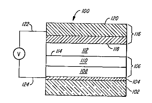
Figure 1 is a schematic diagram of an
internal ~unction organic EL device according to the
invention.
Figure 2 is a plot of light output in mW/cm2
S versus hours of operation.
DescriDtion of Preferred Embodiments
A preferred internal junction organic EL
device 100 satisfying the re~uirements of the invention
is shown in Figure 1. The device is comprised of a
transparent support 102 onto which is coated a
transparent conductive layer 104. The transparent
support and the transparent conductive layer together
form a transparent anode element of the device.
Overlying and in contact with the transparent
conductive layer is a hole injecting and transporting
zone 106. In the preferred form of the invention the
hole injecting zone consists of a hole injecting layer
108 and a hole transporting layer 110. An electron
injecting and transporting zone is provided by layer
112, which forms a junction 114 with the hole injecting
and transporting zone, specifically the hole
transporting layer 110.
Overlying and in contact with the organic
electron injecting and transporting zone, specifically
layer 112, is a cathode 116 comprised of an interfacial
layer 118 located in contact with the electron
injecting and transporting zone, specifically the layer
112. Overlying the interfacial layer of the cathode is
- capping layer 120 chosen to achieve minimal cathode
resistance.
In operation, a voltage source V is connected
to the anode conductive layer 104 by electrical
conductor 122 and to the cathode 116 by electrical
conductor 124. When the voltage source is a continuous
or interrupted DC voltage source the voltage source
-6- 20~6221
biases the cathode negative with respect to the anode
to drive the internal junction organic EL device into
luminescence. When the voltage source is an AC source,
the cathode is biased negative with respect to the
S anode during half of each cycle.
With the cathode biased negative with respect
to the anode electrons are injected into the electron
injecting and transporting zone represented by layer
112. The efficiency of electron injection is
controlled by the interfacial layer 118 of the cathode.
Concurrently, at the anode conductive layer 104 holes
are injected into the hole injecting and transporting
zone 106. Specifically, holes are injected into hole
injecting layer 108 and then transported to the hole
transporting layer 110. Holes are transported within
the hole transporting layer and across the junction 114
to the electron injecting and transporting zone. Hole-
electron recombination occurs in the electron injecting
and transporting zone. As the electron moves out of
the conduction band into a valence band vacancy energy
is released in the form of electromagnetic radiation--
i.e., luminescence occurs.
The present invention is based on the
discovery that a cathode which has at least its
interfacial layer contacting the electron injecting and
transporting zone formed of only a minor amount of
magnesium and a major amount of aluminum can exhibit
both high levels of stability in fabrication and use
and additionally is capable of realizing electron
injection efficiencies comparable to those previously
obtained only by constructing the cathode of greater
than 50 percent (atomic basis) magnesium.
Several alternative cathode constructions are
possible:
~7~ 2~3~;~221
I. The interfacial layer and the backing layer
of the cathode can be of the same composition--i.e.,
the cathode can be a unitary single layer element. In
this instance the cathode contains magnesium and
aluminum in the same proportion throughout.
II. The cathode contains magnesium and aluminum
throughout, but magnesium is present in a reduced
proportion in the backing layer.
III. The cathode contains magnesium and aluminum
in the interfacial layer and aluminum without magnesium
in the backing layer.
IV. The cathode contains magnesium and aluminum
in the interfacial layer and one or a combination of
other metals in the backing layer.
The constant feature of all embodiments is
that the interfacial layer contains magnesium and at
least 80 percent aluminum. (Except as otherwise
indicated, percent is in each instance weight percent
based on total weight.) In the simplest possible
construction the cathode interfacial layer consists
essentially of magnesium and aluminum. At least about
0.05 percent, preferably at least O.lO percent,
magnesium is present in the interfacial layer.
Magnesium can be present in the interfacial layer in a
2S concentration of up to 20 percent, but is preferably
present in a concentration of up to lO percent.
So long as the required concentrations of
magnesium and aluminum are present minor amounts of
other metals can be tolerated. It is generally
preferred that any other metal present have a work
function more positive than that of magnesium, since
magnesium alone is capable of providing the electron
injection efficiencies sought and the stability of a
metal generally increases with increasing work function
3S levels. Minor amounts (< about 5%) of one or more of
- 20~6~1
--8--
the elements commonly present in aluminum electronic
contact systems are specifically contemplated, such as
silicon, copper, titanium, germanium, tin and gallium.
Any thickness of the interfacial layer of the
S cathode capable of covering the surface of the layer
forming the electron injecting and transporting zone
can be employed in constructing the internal junction
organic EL device. Generally, an interfacial layer
thickness of at least 25A, preferably at least 50A and
optimally at least lO0A, is contemplated. The overall
thickness of the cathode can be varied in any
convenient manner to accommodate specific application
requirements. When thin film deposition techniques
such as vacuum vapor deposition or sputtering are
employed to form the cathode, cathode thicknesses of up
to about 2 ~m can be conveniently constructed, with
cathode thicknesses of up to about 5000A being
preferred.
The surprisingly low levels of magnesium
required for efficient device operation allow the
entire cathode to be constructed of a low magnesium
content that lends itself to the fabrication techniques
conventionally employed in constructing aluminum
contact systems for integrated and hydrid circuits.
The aluminum composition is particularly advantageous
for forming patterned cathode arrangements, such as
those required for internal junction organic EL device
arrays. A typical array of this type is demonstrated
by European Patent Application 349,265, published March
14, 1990.
The remaining features of the internal
junction organic EL devices of the invention can take a
variety of forms. Any one of the internal junction
organic EL device constructions disclosed by Tang U.S.
Patent 4,356,429, VanSlyke et al U.S. Patent 4,539,507,
- 2Q46~21
Tang et al U.S. Patent 4,769,292 and Tang et al U.S.
Patent 4,885,211, each cited above, can be combined
with the particular cathode construction of this
invention to produce an improved internal junction
organic EL device. Device constructions shown in these
references in which luminescence occurs through the
cathode are compatible with the invention. The
cathodes in such devices preferably consist of only the
interfacial layer and are optimally less than 300A in
thickness.
In a preferred form of the invention a layer
containing a porphyrinic compound forms the hole
injecting layer of the internal junction organic EL
device. A porphyrinic compound is any compound,
natural or synthetic, which is derived from or includes
the porphyrin structure. Any of the porphyrinic
compounds disclosed by Adler U.S. Patent 3,935,031 or
Tang U.S. Patent 4,356,429 can be employed.
Preferred porphyrinic compounds are those
of structural formula (I):
T ~=~T
~MI--N~
Q~Q
T T2
wherein
Q is -N= or -C(R)=;
M is a metal, metal oxide, or metal halide;
20~ 6221
--10--
R is hydrogen, alkyl, aralkyl, aryl, or alkaryl,
and
Tl and T2 represent hydrogen or together
complete a unsaturated 6 membered ring, which can
S include substituents, such as alkyl or halogen.
Preferred alkyl moieties contain from about 1 to 6
carbon atoms while phenyl constitutes a preferred
aryl moiety.
In an alternative preferred form the
porphyrinic compounds differ from those of structural
formula (I) by substitution of two hydrogen for the
metal atom, as indicated by formula (II):
(II)
T ~ Tl
Highly preferred examples of useful
porphyrinic compounds are metal free phthalocyanines
and metal containing phthalocyanines. While the
porphyrinic compounds in general and the phthalo-
cyanines in particular can contain any metal, the
metal preferably has a positive valence of two or
higher. Exemplary preferred metals are cobalt,
magnesium, zinc, palladium, nickel, and,
particularly, copper, lead, and platinum.
Illustrative of useful porphyrinic
2S compounds are the following:
-- 2Q~6~21
--11--
PC-1 Porphine
PC-2 1,10,15,20-Tetraphenyl-21H,23H-porphine
copper (II)
PC-3 1,10,15,20-Tetraphenyl-21H,23H--porphine
zinc (II)
PC-4 S,10,15,20-Tetrakis(pentafluorophenyl)-
21H,23H-porphine
PC-5 Silicon phthalocyanine oxide
PC-6 Aluminum phthalocyanine chloride
PC-7 Phthalocyanine (metal free)
PC-8 Dilithium phthalocyanine
PC-9 Copper tetramethylphthalocyanine
PC-10 Copper phthalocyanine
PC-ll Chromium phthalocyanine fluoride
PC-12 Zinc phthalocyanine
PC-13 Lead phthalocyanine
PC-14 Titanium phthalocyanine oxide
PC-15 Magnesium phthalocyanine
PC-16 Copper octamethylphthalocyanine
The hole transporting layer of the organic
EL device contains at least one hole transporting
aromatic tertiary amine, where the latter is
understood to be a compound containing at least one
trivalent nitrogen atom that is bonded only to carbon
atoms, at least one of which is a member of an
aromatic ring. In one form the aromatic tertiary
amine can be an arylamine, such as a monoarylamine,
diarylamine, triarylamine, or a polymeric arylamine.
Exemplary monomeric triarylamines are illustrated by
Klupfel et al U.S. Patent 3,180,730. Other suitable
triarylamines substituted with vinyl or vinylene
radicals and/or containing at least one active
hydrogen containing group are disclosed by Brantley
lS et al U.S. Patents 3,567,450 and 3,658,520.
2~622~
-12-
A preferred class of aromatic tertiary
amines are those which include at least two aromatic
tertiary amine moieties. Such compounds include
those represented by structural formula (III):
S (III)
Q1 Q2
G
wherein
Q1 and Q2 are independently aromatic tertiary
amine moieties and
G is a linking group such an arylene, cyclo-
alkylene, or alkylene group or a carbon to carbon
bond.
lS A particularly preferred class of
triarylamines satisfying structural formula (III) and
containing two triarylamine moieties are those
satisfying structural formula (IV):
(IV)
R2
R1- C - R3
R4
2S where
R1 and R2 each independently represents a
hydrogen atom, an aryl group or alkyl group or R1 and
R together represent the atoms completing a
cycloalkyl group and
R3 and R4 each independently represents an aryl
group which is in turn substituted with a diaryl
substituted amino group, as indicated by structural
formula (V):
(V)
R5
- 2~46~1
-13-
S wherein R5 and R6 are independently selected aryl
groups.
Another preferred class of aromatic
tertiary amines are tetraaryldiamines. Preferred
tetraaryldiamines include two diarylamino groups,
such as indicated by formula (V), linked through an
arylene group. Preferred tetraaryldiamines include
those represented by formula (VI).
(VI)
R7 R8
lS
N Aren N
Ar R9
wherein
Are is an arylene group,
n is an integer of from 1 to 4, and
Ar, R7, R8, and R9 are independently
selected aryl groups.
The various alkyl, alkylene, aryl, and
2S arylene moieties of the foregoing structural formulae
(III), (IV), (V), and (VI) can each in turn be
substituted. Typical substituents including alkyl
groups, alkoxy groups, aryl groups, aryloxy groups,
and halogen such as fluoride, chloride, and bromide.
The various alkyl and alkylene moieties typically
contain from about 1 to 5 carbon atoms. The
cycloalkyl moieties can contain from 3 to about 10
carbon atoms, but typically contain five, six, or
seven ring carbon atoms--e.g., cyclopentyl,
3S cyclohexyl, and cycloheptyl ring structures. The
2~221
-14-
aryl and arylene moieties are preferably phenyl and
phenylene moieties.
Representative useful aromatic tertiary
amines are disclosed by Berwick et al U.S. Patent
S 4,175,960 and Van Slyke et al U.S. Patent 4,539,507.
Berwick et al in addition discloses as useful hole
transporting compounds N substituted carbazoles,
which can be viewed as ring bridged variants of the
diaryl and triarylamines disclosed above.
Following the teachings of VanSlyke et al
(II), cited above, it is possible to achieve higher
organic EL device stabilities both during short term
and extended operation by substituting for one or
more of the aryl groups attached directly to a
tertiary nitrogen atom in the aromatic tertiary
amines described above an aromatic moiety containing
at least two fused aromatic rings. The best
combination of both short term (0-50 hours) and long
term (0-300+ hours) of operation are achieved when
the aromatic tertiary amines are those which (1) are
comprised of at least two tertiary amine moieties and
(2) include attached to a tertiary amine nitrogen
atom an aromatic moiety containing at least two fused
aromatic rings. The following is a listing of
exemplary aromatic compounds containing at least two
fused aromatic rings and from 10 to 24 ring carbon
atoms:
Naphthalene,
Azulene,
Heptalene,
as-Indacene,
~-Indacene,
Acenaphthylene,
Phenalene,
Phenanthrene,
2Q~622 1
-15-
Anthracene,
Fluoranthrene,
Acephenathrylene,
Aceantrylene,
S Triphenylene,
Pyrene,
Chrysene,
Naphthacene,
Pleiadene,
Picene,
Perylene,
Pentaphene,
Hexaphene,
Rubicene, and
Coronene.
The fused aromatic ring moieties of the tertiary
amines preferably contain from about 10 to 16 ring
carbon atoms. While unsaturated 5 and 7 membered
rings can be fused to six membered aromatic rings
(i.e., benzene rings) to form useful fused aromatic
ring moieties, it is generally preferred that the
fused aromatic ring moiety include at least two fused
benzene rings. The simplest form of a fused aromatic
ring moiety containing two fused benzene rings is
naphthalene. Therefore, the preferred aromatic ring
moieties are naphthalene moieties, where the latter
is understood to embrace all compounds containing a
naphthalene ring structure. In monovalent form the
naphthalene moieties are naphthyl moieties, and in
their divalent form the naphthalene moieties are
naphthylene moieties.
Illustrative of useful aromatic tertiary
amines are the following:
- 20~6221
-16-
ATA-l 1,1-Bis(4-di-p-tolylaminophenyl)cyclohexane
ATA-2 1,1-Bis(4-di-p-tolylaminophenyl)-4-phenyl-
cyclohexane
ATA-3 4,4'-Bis(diphenylamino)quadriphenyl
ATA-4 Bis(4-dimethylamino-2-methylphenyl)-
phenylmethane,
ATA-5 N,N,N-Tri(p-tolyl)amine
ATA-6 4-(di-p-tolylamino)-4'-[4(di-p-tolylamino)-
styryl]stilbene
ATA-7 N,N,N',N'-Tetra-p-tolyl-4,4'-diaminobi-
phenyl
ATA-8 N,N,N',N'-Tetraphenyl-4,4'-diaminobiphenyl
ATA-9 N-Phenylcarbazole
ATA-10 Poly(N-vinylcarbazole)
ATA-11 4,4'-Bis[N-(1-naphthyl)-N-phenylamino]-
biphenyl
ATA-12 4,4~-Bis[N-(1-naphthyl)-N-phenyl-amino]-p-
terphenyl
ATA-13 4,4'-Bis[N-(2-naphthyl)-N-phenylamino]-
biphenyl
ATA-14 4,4'-Bis[N-(3-acenaphthenyl)-N-phenyl-
amino]biphenyl
ATA-15 1,5-Bis[N-(1-naphthyl)-N-phenylamino]-
naphthalene
ATA-16 4,4'-Bis[N-(9-anthryl)-N-phenylamino]-
biphenyl
ATA-17 4,4~-Bis[N-(1-anthryl)-N-phenylamino]-p-
terphenyl
ATA-18 4,4'-Bis[N-(2-phenanthryl)-N-phenylamino]-
biphenyl
ATA-19 4,4'-Bis[N-(8-fluoranthenyl)-N-phenyl-
amino]biphenyl
ATA-20 4,4'-Bis[N-(2-pyrenyl)-N-phenylamino]bi-
phenyl
21!~6221
-17-
ATA-21 4,4'-Bis[N-(2-naphthacenyl)-N-phenylamino]-
biphenyl
ATA-22 4,4'-Bis[N-(2-perylenyl)-N-phenylamino]-
biphenyl
ATA-23 4,4'-Bis[N-(1-coronenyl)-N-phenylamino]-
biphenyl
ATA-24 2,6-Bis(di-~-tolylamino)naphthalene
ATA-25 2,6-Bis[di-(1-naphthyl)amino]naphthalene
ATA-26 2,6-Bis[N-(1-naphthyl)-N-(2-naphthyl)-
amino]naphthalene
ATA-27 4,4~-Bis[N,N-di(2-naphthyl)amino]terphenyl
ATA-28 4,4'-Bis{N-phenyl-N-[4-(1-naphthyl)phenyl]-
amino}biphenyl
ATA-29 4,4'-Bis[N-phenyl-N-(2-pyrenyl)amino]bi-
phenyl
ATA-30 2,6-Bis[N,N-dit2-naphthyl)amine]fluorene
ATA-31 4,4~-Bis(N,N-di-p-tolylamino)terphenyl
ATA-32 Bis(N-1-naphthyl)(N-2-naphthyl)amine
Any conventional electron injecting and
transporting compound or compounds can be employed in
forming the layer of the organic electroluminescent
medium adjacent the cathode. This layer can be formed
S by historically taught luminescent materials, such as
anthracene, naphthalene, phenanthrene, pyrene,
chrysene, and perylene and other fused ring luminescent
materials containing up to about 8 fused rings as
illustrated by Gurnee et al U.S. Patent 3,172,862,
Gurnee U.S. Patent 3,173,050, Dresner, ~Double
Injection Electroluminescence in Anthracene~, BS~
Review, Vol. 30, pp. 322-334, 1969; and Dresner U.S.
Patent 3,710,167, cited above. Although such fused
ring luminescent materials do not lend themselves to
forming thin (e 1 mm) films and therefore do not lend
themselves to achieving the highest attainable EL
device performance levels, organic EL devices
- 20~6221
-18-
incorporating such luminescent materials when
constructed according to the invention show
improvements in performance and stability over
otherwise comparable prior art EL devices.
S Among electron transporting compounds useful
in forming thin films are the butadienes, such as 1,4-
diphenylbutadiene and tetraphenylbutadiene; coumarins;
and stilbenes, such as trans-stilbene, disclosed by
Tang U.S. Patent 4,356,429, cited above.
Still other thin film forming electron
transporting compounds which can be used to form the
layer adjacent the cathode are optical brighteners,
particularly those disclosed by VanSlyke et al U.S.
Patent 4,539,507, cited above. Useful optical
brighteners include those satisfying structural
formulae (VII) and (VIII):
(VII)
R ~ Z ~ R4
or
(VIII)
Rl ~ ~ ~ y ~
whereln
Rl, R2, R3, and R4 are individually
hydrogen; saturated aliphatic of from 1 to 10 carbon
atoms, for example, propyl, t-butyl, heptyl, and the
like; aryl of from 6 to 10 carbon atoms, for example,
phenyl and naphthyl; or halo such as chloro, fluoro,
and the like; or Rl and R2 or R3 and R4 taken
~ ~ ~ 6 2 ~ 1
-
--19--
together comprise the atoms necessary to complete a
fused aromatic ring optionally bearing at least one
saturated aliphatic of from 1 to 10 carbon atoms,
such as methyl, ethyl, propyl and the like;
S R5 is a saturated aliphatic of from 1 to 20
carbon atoms, such as methyl, ethyl, n-eicosyl, and
the like; aryl of from 6 to 10 carbon atoms, for
example, phenyl and naphthyl; carboxyl; hydrogen;
cyano; or halo, for example, chloro, fluoro and the
like; provided that in formula (VII) at least two of
R3, R4 and R5 are saturated aliphatic of from 3 to 10
carbon atoms, e.g., propyl, butyl, heptyl and the
like;
Z iS -O-, -NH-, or -S-; and
lS Y is
-R6-(CH=CH-)R6-,
J=X
~ Y
- ~ m
, -CH=CH-,
-(CH=CH-)R6-(CH=CH-) n~ '
~/ ' Z "
or
~S~
whereln
20~622~ :
-
-20-
m is an integer of from 0 to 4;
n is arylene of from 6 to 10 carbon atoms,
for example, phenylene and naphthylene; and
Z' and Z- are individually N or CH.
S As used herein ~aliphatic~ includes substituted
aliphatic as well as unsubstituted aliphatic. The
substituents in the case of substituted aliphatic
include alkyl of from 1 to 5 carbon atoms, for
example, methyl, ethyl, propyl and the like; aryl of
from 6 to 10 carbon atoms, for example, phenyl and
naphthyl; halo, such as chloro, fluoro and the like;
nitro; and alkoxy having 1 to 5 carbon atoms, for
example, methoxy, ethoxy, propoxy, and the like.
Still other optical brighteners that are
lS contemplated to be useful are listed in Vol. 5 of
Chemistry of Synthetic ~yes, 1971, pages 618-637 and
640. Those that are not already thin-film-forming
can be rendered so by attaching an aliphatic moiety
to one or both end rings.
Particularly preferred for use in forming
the electron injecting and transporting layers of the
organic EL devices of this inventions are metal
chelated oxinoid compounds, including chelates of
oxine (also commonly referred to as 8-quinolinol or
2S 8-hydroxyquinoline). Such compounds exhibit both
high levels of performance and are readily fabricated
in the form of thin films. Exemplary of contemplated
oxinoid compounds are those satisfying structural
formula (IX):
(IX)
,Z~ ~ M e ~ n = ,Z~o~ M e
~ n - ~ n
~ 2Q~6221
-21-
wherein
Me represents a metal;
n is an integer of from 1 to 3; and
Z independently in each occurrence represents
S the atoms completing a nucleus having at least two
fused aromatic rings.
From the foregoing it is apparent that the
metal can be monovalent, divalent, or trivalent
metal. The metal can, for example, be an alkali
metal, such as lithium, sodium, or potassium; an
alkaline earth metal, such as magnesium or calcium;
or an earth metal, such as boron or aluminum.
Generally any monovalent, divalent, or trivalent
metal known to be a useful chelating metal can be
employed.
Z completes a heterocyclic nucleus
containing at least two fused aromatic rings, at one
of which is an azole or azine ring. Additional
rings, including both aliphatic and aromatic rings,
can be fused with the two required rings, if
required. To avoid adding molecular bulk without
improving on function the number of ring atoms is
preferably maintained at 18 or less.
Illustrative of useful chelated oxinoid
compounds are the following:
C0-1 Aluminum trisoxine
[a.k.a., tris(8-quinolinol) aluminum]
C0-2 Magnesium bisoxine
[a.k.a., bis(8-quinolinol) magnesium]
C0-3 Bis[benzo{f}-8-quinolinol] zinc
C0-4 Aluminum tris(5-methyloxine)
[a.k.a., tris(5-methyl-8-quinolinol)
aluminum]
C0-5 Indium trisoxine
[a.k.a., tris(8-quinolinol) indium]
r ; 2 ~D ~9 6 ~ 2 ~
-22-
C0-6 Lithium oxine
[a.k.a., 8-quinolinol lithiuml
C0-7 Gallium tris(5-chlorooxine)
[a.k.a, tris(5-chloro-8--quinolinol)
gallium]
C0-8 Calcium bis(5-chlorooxine)
[a.k.a, bis(5-chloro-8-quinolinol) calcium]
C0-9 Poly[zinc (II)-bis(8-hydroxy-5-
quinolinyl)methane]
C0-10 Dilithium epindolidione
It is possible to modify the wavelength of
emission from the electron injecting and transporting
zone and, in some instances, to increase the stability
of the organic EL device in operation by incorporating
in the electron injecting and transporting zone a dye
capable of emitting light in response to hole-electron
recombination. To be useful for this purpose the dye
must have a bandgap no larger than that of the host
material in which it is dispersed and a reduction
potential less negative than that of the host material.
Tang et al U.S. Patent 4,769,292, describes internal
junction organic EL devices containing dyes selected
from a variety of classes dispersed in electron
injecting and transporting zone host materials.
In the organic EL devices of the invention it
is possible to maintain a current density compatible
with efficient light emission while employing a
relatively low voltage across the electrodes by
limiting the total thickness of the organic
electroluminescent medium to less than 1 ~m (10,000
Angstroms). At a thickness of less than 1 ~m an
applied voltage of 20 volts results in a field
potential of greater than 2 X 10⁵ volts/cm, which is
compatible with efficient light emission. An order of
magnitude reduction (to 0.1 ~m or 1000 Angstroms) in
20~21
-23-
thickness of the organic electroluminescent medium,
allowing further reductions in applied voltage and/or
increase in the field potential and hence current
density, are well within device construction
S capabilities.
One function which the organic
electroluminescent medium performs is to provide a
dielectric barrier to prevent shorting of the
electrodes on electrical biasing of the EL device.
Even a single pin hole extending through the organic
electroluminescent medium will allow shorting to occur.
Unlike conventional EL devices employing a single
highly crystalline electroluminescent material, such as
anthracene, for example, the EL devices of this
invention are capable of fabrication at very low
overall organic electroluminescent medium thicknesses
without shorting. One reason is that the presence of
three superimposed layers greatly reduces the chance of
pin holes in the layers being aligned to provide a
continuous conduction path between the electrodes.
This in itself permits one or even two of the layers of
the organic electroluminescent medium to be formed of
materials which are not ideally suited for film
formation on coating while still achieving acceptable
2S EL device performance and reliability.
The preferred materials for forming the
organic electroluminescent medium are each capable of
fabrication in the form of a thin film--that is,
capable of being fabricated as a continuous layer
having a thickness of less than 0.5 ~m or 5000
Angstroms.
When one or more of the layers of the organic
electroluminescent medium are solvent coated, a film
forming polymeric binder can be conveniently co-
deposited with the active material to assure a
20~6221
-24-
continuous layer free of structural defects, such as
pin holes. If employed, a binder must, of course,
itself exhibit a high dielectric strength, preferably
at least about 2 X 10⁶ volt/cm. Suitable polymers can
S be chosen from a wide variety of known solvent cast
addition and condensation polymers. Illustrative of
suitable addition polymers are polymers and copolymers
(including terpolymers) of styrene, ~-butylstyrene, N-
vinyl carbazole, vinyltoluene, methyl methacrylate,
methyl acrylate, acrylonitrile, and vinyl acetate.
Illustrative of suitable condensation polymers are
polyesters, polycarbonates, polyimides, and
polysulfones. To avoid unnecessary dilution of the
active material binders are preferably limited to less
lS than 50 percent by weight, based on the total weight of
the material forming the layer.
The preferred active materials forming the
organic electroluminescent medium are both film forming
materials and capable of vacuum vapor deposition.
Extremely thin defect free continuous layers can be
formed by vacuum vapor deposition. Specifically,
individual layer thicknesses as low as about 50
Angstroms can be present while still realizing
satisfactory EL device performance. Employing a vacuum
vapor deposited porphorinic compound as a hole
injecting layer, a film forming aromatic tertiary amine
as a hole transporting layer, and a chelated oxinoid
compound as an electron injecting and transporting
layer, thicknesses in the range of from about 50 to
5000 Angstroms are contemplated, with layer thicknesses
in the range of from 100 to 2000 Angstroms being
preferred. It is generally preferred that the overall
thickness of the organic electroluminescent medium be
at least about 1000 Angstroms.
~ r
_ 2Q9~6221
-25-
The anode of the organic EL device can take
any convenient conventional form. Where it is intended
to transmit light from the organic EL device through
the anode, this can be conveniently achieved by coating
S a thin conductive layer onto a light transmissive
substrate--e.g., a transparent or substantially
transparent glass plate or plastic film. In one form
the organic EL devices of this invention can follow the
historical practice of including a light transmissive
anode formed of tin oxide or indium tin oxide (ITO)
coated on a glass plate, as disclosed by Gurnee et al
U.S. Patent 3,172,862, Gurnee U.S. Patent 3,173,050,
Dresner, ~Double Injection Electroluminescence in
Anthracene~, B~ Review, Vol. 30, pp. 322-334, 1969;
lS and Dresner U.S. Patent 3,710,167, cited above. While
any light transmissive polymeric film can be employed
as a substrate, Gillson U.S. Patent 2,733,367 and
Swindells U.S. Patent 2,941,104 disclose polymeric
films specifically selected for this purpose.
As employed herein the term ~light
transmissive~ means simply that the layer or element
under discussion transmits greater than 50 percent of
the light of at least one wavelength it receives and
preferably over at least a 100 nm interval. Since both
specular (unscattered) and diffused (scattered) emitted
light are desirable device outputs, both translucent
and transparent or substantially transparent materials
are useful. In most instances the light transmissive
layers or elements of the organic EL device are also
colorless or of neutral optical density--that is,
exhibiting no markedly higher absorption of light in
one wavelength range as compared to another. However,
it is, of course, recognized that the light
transmissive electrode supports or separate
3S superimposed films or elements can be tailored in their
_ 2~46221
light absorption properties to act as emission trimming
filters, if desired. Such an electrode construction is
disclosed, for example, by Fleming U.S. Patent
4,035,686. The light transmissive conductive layers of
S the electrodes, where fabricated of thicknesses
approximating the wavelengths or multiples of the light
wavelengths received can act as interference filters.
~xam~les
The invention and its advantages are further
~0 illustrated by the specific examples which follow. The
term ~cell~ as employed in the examples denotes an
organic EL device. Examples with a number bearing the
suffix E represent embodiments of the invention while
Examples with a number bearing the suffix C are
lS included for the purpose of comparing variations in
construction.
~xam~le 1~ Preparation of an Internal Junction
Organic Device with a Two Layer Cathode
An internal junction organic EL device
containing a two layer cathode was prepared in the
following manner:
a) A transparent anode of ITO coated glass was
ultrasonically cleaned in a 3% solution of DeconexTM
12PA detergent (Borer Chemie AG) for a few minutes. It
2S was then rinsed with deionized water and isopropyl
alcohol, and finally immersed in toluene vapor for
about 15 minutes.
b) A hole injecting layer (375A) of copper
phthalocyanine was deposited onto the anode by vacuum
deposition. It was sublimed from a quartz boat heated
by a tungsten filament.
c) A hole transporting layer (375A) of N,N,N',N'-
tetra-p-tolyl-4,4'-diaminobiphenyl was deposited on top
_ 2Q~6221
-27-
of the copper phthalocyanine. It was also evaporated
from a quartz boat.
d) An electron injecting and transporting layer
(600A) of tris(8-quinolinol) aluminum was then
S deposited on top of the hole transporting layer, again
by sublimation from a quartz boat.
e) On top of the tris(8-quinolinol) aluminum was then
deposited a mixed metal (200A) of magnesium and
aluminum in a volume ratio of l:50. This was
accomplished by subliming Mg from a resistively heated
tantalum boat while simultaneously evaporating aluminum
from an electron beam heated graphite crucible.
f) On top of the mixed metal was then deposited 2000A
of pure aluminum, again from an electron beam heated
graphite crucible, as a capping layer, steps e) and f)
together completing the cathode.
When a negative voltage was connected to the
cathode and the anode was connected to ground,
luminescence was visible through the transparent anode.
The efficiency of the device (optical output in watts
per ampere of electrical current passing through the
cell) was 0.014 Watt/Amp. At a current density of 20
mA/cm2, the drive voltage was 9.l volts and the
emission intensity was 0.28 mW/cm2. The cell
characteristics are shown in Table I.
~amDle 2C A Single Layer Cathode of Pure Aluminum.
An internal junction organic EL device was
constructed identically to that of Example lE, except a
: pure aluminum layer (2000A) was deposited on top of the
organic films. The efficiency of this cell was 0.0l0
W/A. At 20 mA/cm2 the drive voltage was 12.5 volts and
the light intensity was 0.20 mW/cm2 (Table I). The
poorer characteristics of this cell demonstrate that
for optimum performance, magnesium needs to be mixed
with aluminum.
20~622~1
-
-28-
~x~m~les 3~ 4C an~ 5C Single Layer Mg:Al Cathodes
- with a Range of Concentrations
Internal junction organic EL devices were
constructed identically to that of Example lE, except
S the Mg:Al volume ratios were 1:20, 1:1 and 10:1. The
thickness of the mixed layers in each case was about
2000A and no aluminum capping layer was deposited.
These devices exhibited comparable behavior to the
device of Example lE as set forth in Table I and
demonstrate that the electron injection efficiency is
only minimally dependent on the magnesium concentration
for Mg:Al cathodes.
~xam~les 6~. 7C and 8C Two layer Al:Mg/Al Cathodes
with a Range of Concentrations.
Internal junction organic El devices were
constructed identically to that of Example lE, except
that the concentration of the mixed layer adjacent to
the organic electroluminescent medium was varied. As
shown in Table I, these cells show only a m;n;m~l
concentration dependence and behave comparably to
Example lE. This demonstrates that even though the
mixed layer thickness is quite thin, the cathode
properties are relatively unaffected.
~xam~les 9C; lOC ~n~ llC Comparison of Al:Mg with Mg:Ag
Cathodes
Two layer cathodes of Al:Mg~Al and Mg:Ag/Al
were prepared as in Example lE, except that in one
sample Ag was mixed with magnesium in order to compare
its binder properties with that of aluminum. The
silver was evaporated in the same manner as the
aluminum from an electron beam heated graphite
crucible. As shown in Table I, the 62.4% magnesium in
silver cathode behaved comparable to the 81.5%
magnesium in aluminum cathode, however, all attempts at
204622~
,
-29-
making a cathode with a magnesium content of less than
50% in silver were unsuccessful due to shorting of the
device. This demonstrates that Mg:Al cathodes behave
comparably to Mg:Ag cathodes (with high Mg content) but
S have the added virtue that the concentration of the Mg
can be quite low.
~x~m~le 12 Operational Stability of Example 1-11
Cells
The internal junction organic EL devices of
Examples 1-11 were stability tested under constant
current conditions using 1 kHz AC excitation. The
current was set at a level which produced the same
light output as 20 mA/cm2 direct current. Figure 2
shows a plot of the normalized light output versus time
~S for the cell described in Example lE. The light output
clearly stayed above 0.1 mW/cm2 for over 1000 hours
(initial light output level 0.28 mW/cm2). All of the
Example 1-11 cells exhibited about the same normalized
drop in light output level, as shown in Table II, with
the loss in light output being about 40% after 300
hours operation. The drive voltage increased in each
instance, reflecting an increasing cell resistance with
continued operation. However, all of the example cells
showed a voltage rise of <0.5 volt AC over 300 hours of
2S operation. For the 100% aluminum cathode, the voltage
rise was more rapid during operation (increasing about
2 volts AC in the first 300 hours), and the initial
efficiency was considerably less, demonstrating the
need for a small amount of magnesium to be incorporated
in the cathode to achieve optimum performance.
These results demonstrate cathode composition
independence on the stability of electroluminescent
cells which employ a mixed metal cathode of Mg and Al.
Further the mixed metal layer can be quite thin, and a
_ 20~6221
-30-
pure aluminum capping layer can be deposited to
complete the cathode, but is not required.
TABT~ T
Example Number of Weight Efficiency Voltage at
SNo. cathode percent (W/A) 20 mA/cm2
layers Mg (Volts)
lE 2 1.3 0.014 9.1
2C 1 0.0 0.01012.5
3E 1 3.4 0.015 9.3
4C 1 39.2 0.014 9.2
5C 1 86.6 0.015 8.6
6E 2 3.4 0.015 9.2
7C 2 39.2 0.016 8.6
8C 2 86.6 0.016 8.4
lS 9C 2 81.5 0.016 8.1
lOC 2* 62.4 0.017 7.7
llC 2* 14.2 - - - - shorted - - -
*mixed layer is MgAg
TABT .E T T
Initial % Initial
Example No. of Weight light light out- Voltage
No. cathode % Mg output put after rise (AC
layers (mW/cm2) 300 hours volts)
lE 2 1.3 0.28 62 0.2
2S 2C 1 0.0 0.21 60 2.0
3E 1 3.4 0.30 67 0.4
4C 1 39.2 0.28 63 0.4
5C 1 86.6 0.29 63 0.7
6E 2 3.4 0.30 64 0.4
7C 2 39.2 0.31 64 0.4
8C 2 86.6 0.32 63 0.6
9C 2 81.5 0.32 59 0.4
lOC 2* 62.4 0.33 62 0.4
llC 2* 14.2 - - - - - - shorted - - - -
20~ 6221
-31-
*mixed layer is MgAg
The invention has been described in detail
with particular reference to preferred embodiments
thereof, but it will be understood that variations and
S modifications can be effected within the spirit and
scope of the invention.