Note: Descriptions are shown in the official language in which they were submitted.
2~4 6250
27879-68
TITLE OF THE INVENTION
HYBRID CIRCUIT HAVING A TWO-WIRE/FOUR-WIRE
CONVERTING FUNCTION
FIELD OF INVENTION
The present invention generally relates to a hybrid
circuit having a two-wire/four-wire converting function, and more
particularly to a hybrid circuit having a digital balancing
circuit.
BRIEF DESCRIPTION OF THE DRAWINGS
Other objects, features and advantages of the present
invention will become apparent from the following detailed
description when read in conjunction with the accompanying
drawings, in which:
FIGURE 1 is a block diagram of a hybrid circuit having a
hybrid transformer in a PCM channel unit;
FIGURE 2 is a block diagram of a hybrid circuit having
an active hybrid circuit in a PCM channel unit;
FIGURE 3 is a circuit diagram of an active hybrid
circuit shown in FIGURE 2;
FIGURE 4 is a block diagram of a balancing network
circuit;
FIGURE 5 is a block diagram of an overview of a hybrid
circuit of the present invention;
FIGURE 6 is a block diagram of a first preferred
embodiment of the present invention;
FIGURE 7 is a circuit diagram of an impedance
approximation circuit used with a hybrid transformer employed;
. . ~
2046250
2 27879-68
FIGURE 8 is a circuit diagram of an impedance
approximation circuit used with an active hybrid circuit employed;
FIGURE 9 is a block diagram of a digital balancing
circuit;
FIGURE 10 is a block diagram of a second preferred
embodiment of the present invention;
FIGURE 11 is a block diagram of an interpolation filter
used in the configuration shown in FIGURE 10; and
FIGURE 12 is a graph of a loss characteristic of the
interpolation filter shown in FIGURE 10.
DESCRIPTION OF THE RELATED ART
A conventional two-wire PCM channel unit having a two-
wiretfour-wire converting function includes a power receiving
unit, and a power supply unit, which supplies a voltage of -48V to
a terminal. Conventionally, these units are coupled with each
other by a hybrid transformer having the two-wire/four-wire
converting function.
FIGURE 1 is a block diagram of a related hybrid circuit
in a PCM channel unit using a hybrid transformer. As shown, the
PCM channel unit includes terminals TIP and RING for a two-wire
line, and signal sending and receiving terminals SOUT and RIN for
a four-wire line. Further, the PCM channel unit includes a hybrid
transformer 61, rough gain adjustment circuit 62 and 63, a
conversion block 64, an adder 67, a balancing circuit 68,
equalizers 69 and 70, a compressing unit 71, and de-compressing
(expanding) unit 72. The conversion block 64 is composed of an
analog-to-digital (A/D) converter 65, and a digital-to-analog
(D/A) converter 66. Each of the equalizers 69 and 70 executes a
,f
- 2a 2046250 27879-68
fine level adjustment procedure and a loss equalizing procedure.
The compressing unit (L/~) 71 converts a linear code L into a
compressed code based on the ~-rule, and the expanding unit (~/L)
72 converts the ~-rule based compressed code into the linear code
L. The functions
. .. --
,~
2046250
1 of the elements 67 - 72 are implemented by a digital
signal processor.
The compressed code based on the lu rule is
input to the expander 72 via the signal receiving
terminal RIN. The expander 72 converts the received
compressed code into a linear code, which is subjected
to the fine level adjustment procedure and the loss
equalizing procedure by the equalizer 70. An output
signal of the equalizer 70 is input to the D/A converter
66 and the balancing circuit 68. The D/A converter 66
converts the digital signal into an analog signal, which
is amplified by the rough gain adjustment circuit 63 and
sent out to the two-wire line coupled to the terminals
TIP and RING via the hybrid transformer 61.
Meanwhile, an analog signal transmitted via
the terminals TIP and RING is input to the A/D converter
65 via the hybrid transformer 61 and the rough gain
adjustment circuit 62. Then, the analog signal is
converted into a digital signal by the A/D converter 65,
and applied to a plus terminal of the adder 67. The
balancing circuit 68 outputs a pseudo echo to a minus
terminal of the adder 67. Thereby, a return echo
contained in the signal from the A/D converter 65 is
canceled by the pseudo echo. An output signal of the
adder 67 is input, via the equalizer 69, to the
compressor 71, which converts the output signal from the
adder 67 into the compressed code based on the lu rule.
The compressed code is sent out via the terminal SOUT.
The balancing circuit 68 produces a transform
characteristic identical to that of an echo return
route. The balancing circuit 68 can be realized,
together with other functions, by a digital signal
processor. An equalizing function (EQ), an
interpolation filtering function (FIL), and a transfer
function (Ht) of an echo return route are realized by
digital processing. It will be noted that the echo
return route includes the D/A converter 66, the rough
f
~f 2046250
1 gain adjustment circuit 63, the hybrid transformer 61,
the rough gain adjustment circuit 62 and the A/D
converter 64, and the return echo pass through these
elements in this order. As has been described
previously, the adder 67 functions to cancel the return
echo by the pseudo echo generated by the balancing
circuit 68.
FIG.2 is a block diagram of another related
hybrid circuit in the PCM channel unit using an active
hybrid circuit. The PCM channel unit includes a
non-inverting amplifier 81, an inverting amplifier 82, a
differential amplifier 83, rough gain adjustment
circuits 84 and 85, a conversion circuit 86, an adder
89, a balancing circuit 90, equalizers 91 and 92, a
compressor 93, and an expander 94. The conversion
circuit 86, which includes an A/D converter 87 and a D/A
converter 88, operates in the same way as the conversion
circuit 64 shown in FIG.1. The compressor 93 and the
expander 94 function in the same way as the compressor
20 71 and the expander 72 shown in FIG.1. Further, the
hybrid circuit shown in FIG.2 includes a resistor R1 and
a capacitor C1, both of which form a terminating
impedance. Generally, the elements 89 - 94 are realized
by a digital signal processor.
The balancing circuit 90 has the equalizing
function (EQ) and the interpolation filtering function
(FIL) in the same way as the balancing circuit 68 shown
in FIG.l. Further, the balancing circuit 90 has a
transfer function (Ha) of an echo return route, which
function is different from that of the balancing circuit
68. The echo return route in the configuration shown in
FIG.2 includes the D/A converter 88, the rough gain
adjustment circuit 85, the non-inverting amplifiers 81
and 82, the differential amplifier 83, the rough gain
adjustment circuit 84 and the A/D converter 87, and the
return echo passes through these elements in this
order. The balancing circuit 90 generates a pseudo
-
~ 2046250
1 echo, which is subtracted from the signal from the A/D
converter 87, so that the return echo contained in the
output from the A/D converter 87 is canceled.
FIG.3 is a block diagram of the active hybrid
circuit shown in FIG.2. In FIG.3, those parts which are
the same as those shown in FIG.2 are given the same
reference numerals. The active hybrid circuit shown in
FIG.3 includes transistors 95 and 96, an adder 97, and
an echo canceller 98. A voltage of -48V is applied to
the terminal RING via the transistor 96, so that
electricity is supplied to the two-wire line coupled to
the terminals TIP and RING.
The transfer function Ht of the echo return
route formed in the hybrid circuit using the hybrid
transformer 61 shown in FIG.1 is expressed as follows:
Ht = (1/4)[(Z - Rl)/(Z + Rl)~ (1)
where Z is an impedance obtained by viewing the two-wire
line from the terminals TIP and RING, and Rl is a
standard impedance of the hybrid transformer 61, which
is twice a resistor connected between an intermediate
tap of the hybrid transformer 61 and the system ground.
The transfer function Ha of the echo return
route formed in the hybrid circuit using the active
hybrid circuit shown in FIGS.2 and 3 is expressed as
follows:
Ha = (~Z-Z')/(Z + Z') (2)
where Z' is the impedance of a series circuit consisting
of the resistor Rl and the capacitor Cl, and ~ is a
constant having the dimension of admittance. It can be
seen from the above description that the balancing
circuit 90 must be formed in a way different from that
of the balancing circuit 68.
In order to realize a return echo cancelling
circuit in the analog domain, a circuit is used which is
composed of an operational amplifier, a resistor and a
capacitor. FIG.4 is a circuit diagram of the balancing
circuit 90 used for the active hybrid circuit type. An
i
2046250
6 27879-68
operational amplifier has a non-invertlng input terminal which is
grounded, and an inverting lnput terminal whlch recelves an lnput
signal via a resistor R. The impedance between the inverting
input terminal of the operatlonal amplifier 99 and an output
terminal thereof is indlcated by Zx. Thus, the following formulas
are obtained taking into account the aforementloned formula (2):
Zx = (Z .Z')/(Z + Z')
R = 1/a.
Thus, if the above two formulas stand, it is possible for the
adder 97 to cancel the return echo.
Generally, the impedance Z obtained by viewlng the two-
wlre llne depends on the length and type of cable. Thus, a plura-
llty of impedance Zx elements are prepared in order to conform to
typical types of cable, and are selectively used. The most typi-
cal impedance Zx is equal to Z'/2, in which Z' is a standard
terminating lmpedance of a system. The lmpedance Z is equal to
the impedance Z' if cables and so on are ideal ones.
A scheme is known in which a circuit for cancelling a
return echo in the two-wire/four-wire converting means using the
hybrid transformer is formed of a digital signal processor (see
Alfred Fettweis, "WAVE DIGITAL FILTER: THEORY AND PRACTICE",
Proceedings of the IEEE, Vol. 74, No. 2, Feb., 1986, pp. 314.
Recently, the active hybrid circuit type has been more
widely used, and many hybrid transforms which are working tend to
be replaced by the active hybrid circuit type. Under such a
circumstance, it is required to provide a PCM channel unit in
conformity with both the hybrid transformer type and the active
hybrid circuit type. In order to meet this requirement, lt may be
possible to provide two balanclng circuits 68 and 90 in the PCM
channel unit. However, this increases the
20462S0
1 size and cost of the PCM channel unit. Further, in the
case where the transfer function Ha used in the active
hybrid circuit type is realized by only digital signal
processing, if a large-amplitude signal is input to the
A/D converter 87 of the PCM channel unit, the A/D
converter 87 will overflow, so that the output signal of
the A/D converter 87 will be distorted.
SUMMARY OF THE INVENTION
It is a general object of the present
invention to provide a hybrid circuit in which the
above-mentioned disadvantages are eliminated.
A more specific object of the present
invention is to provide a simple and less expensive
hybrid circuit having a balancing circuit in conformity
with both the hybrid transformer type and the active
hybrid circuit type.
The above-mentioned objects of the present
invention are achieved by a hybrid circuit comprising:
two-wire/four-wire conversion means for
forming an interface between a two-wire line and a
four-wire line, the four-wire line having a signal
receiving terminal and a signal sending terminal; and
digital balancing means, operatively coupled
to the two-wire/four-wire conversion means, for
canceling a return echo passing through an echo return
route including the two-wire/four-wire conversion means,
the digital balancing means comprising:
first means for determining values of elements
of a ladder type circuit composed of resistors and
capacitors, the ladder type circuit corresponding to an
original equivalent circuit having an impedance obtained
by viewing the two-wire line from the two-wire/four-wire
conversion means;
second means, operatively coupled to the first
means, for generating an impedance function of the
original equivalent circuit in the form of a z function
.,
,
8 204 6250 27879-68
in accordance with a bilinear transform using an over-sampling
frequency;
third means, operatively coupled to the second means,
for generating filter coefficients of a digital filter by
inserting the impedance function into a transfer function of the
echo return route; and
fourth means, which is coupled to the third means and
has the digital filter, for generating, from a signal transferred
via the signal receiving terminal, an echo cancel signal by the
digital filter having the filter coefficients generated by the
third means and for canceling the return echo by the echo cancel
signal.
DESCRIPTION OF THE PREFERRED EMBODIMENTS
Referring to FIGURE 5, the hybrid circuit of the present
invention includes a two-wire/four-wire conversion unit 1, a
digital balancing circuit 2 and an interpolation filter 3. TIP
and RING are terminals for the two-wire line (cable~, and SOUT and
RIN are respectively signal sending and receiving terminals for
the four-wire line (cable). The digital balancing circuit 2,
which can be implemented by a digital signal processor, has the
first, second and third functions, which will be described below.
The first function of the digital balancing circuit 2 determines,
on the basis of a cable condition about the two-wire line, the
terminating impedance and so on, the values of elements forming a
ladder type network composed of a plurality of capacitors and
resistors which represent an impedance obtained by viewing the
two-wire line from the conversion unit 1. The second function
transforms the determined element values into an impedance
.......
- 8a 204 6250 27879-68
function of the z function by a bilinear transform. The third
function inserts the impedance function into a transfer function
in order to generate filter coefficients. With this arrangement,
it is possible to cancel a return echo leaking from the signal
receiving terminal RIN of the four-wire line to the signal sending
terminal SOUT thereof by the same circuit configuration in common
to the hybrid transformer and the active hybrid circuit.
A description will now be given of a first preferred
embodiment of the present invention with
_
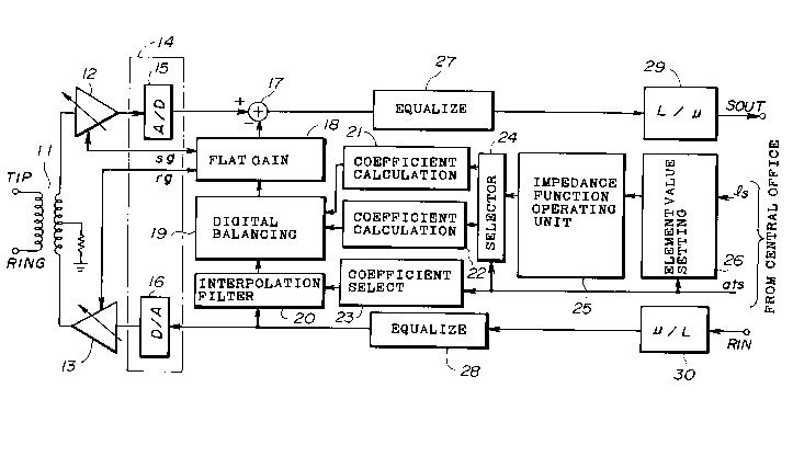
- 9 ~046250
1 reference to FIG.6. The configuration shown in FIG.6
includes a hybrid transformer 11, rough gain adjustment
circuits 12 and 13, a conversion circuit 14, an A/D
converter 15, a D/A converter 16, an adder 17, a flat
gain operation unit 18, a digital balancing circuit 19,
an interpolation filter operation unit 20, a hybrid
transformer coefficient calculating unit 21, an active
hybrid circuit coefficient calculating unit 22, an
interpolation filter coefficient selecting unit 23, a
selector 24, an impedance function operating unit 25, an
element value setting unit 26, two equalizers 27 and 28,
a compressor 29 and an expander 30. Further, the
configuration shown in FIG.6 includes the terminals DIP
and RING for the two-wire line, and signal sending and
receiving terminals SOUT and RIN for the four-wire
line. The above structural elements 17 - 30 can be
realized by a digital signal processing circuit, such as
a digital signal processor.
The embodiment shown in FIG.6 uses a hybrid
transformer 11 which forms a two-wire/four-wire
conversion circuit. The two-wire line is connected to
the terminals TIP and RING. Line information ls and
discrimination information ats are input to the element
value setting unit 26 from a central office (not shown
for the sake of simplicity) in a PCM system. The line
information ls indicates a cable condition such as the
length and type of the two-wire line (cable), and a line
(cable) terminating impedance. The discrimination
information ats indicates the type of the hybrid circuit
(that is, whether the hybrid transformer type or the
active hybrid circuit type is used). The element value
setting unit 26 determines the values of elements which
form a circuit shown in FIG.8. The element values
determined by the element value setting unit 26 are
input to the impedance function operating unit 25. The
discrimination information ls is input to the selector
24 and the coefficient selecting unit 23.
- lO - 2046250
Information sg roughly indicat;n~ ~ 5ig nc~l
sending gain and information rg roughly indicating a
signal receiving gain are input to the rough gain
adjustment circuits 12 and 13, respectively, and to the
5 flat gain operating unit 18. The information sg and rg
are used for controlling the gains of the circuits 12
and 13, respectively. The flat gain operating unit 18
controls the gain of a signal applied to the minus
terminal of the adder 17 on the basis of the information
10 sg and rg. The information sg and rg are generated by
the digital signal processor which forms the operation
units and coefficient calculating units shown in FIG.6.
The routes through which the information sg and rg are
transmitted are simply depicted for the sake of
15 simplicity.
When the hybrid transformer 11 is used as the
two-wire/four-wire conversion circuit, an equivalent
circuit obtained by viewing the two-wire line side from
the terminals TIP and RING is a ladder circuit which
20 includes resistors R2 and R3 and capacitors C2 and C3
like an impedance approximation circuit shown in FIG.7.
The equivalent circuit based on such an impedance
approximation circuit has a fixed element value such
that C3 = 2.16 llF. The other elements C2 and the
25 resistors R2 and R3 depend on the cable condition, such
as the cable length and cable type. However, the
impedance approximation circuit substantially shows the
impedance of a pair cable having a remote end which is
terminated by an impedance equal to 600~2 + 2.16 luF or
30 goo Q + 2.16 ,uF.
Meanwhile, the balancing circuit used with the
active hybrid circuit employed corresponds to an
impedance approximation circuit shown in FIG.8, which
shows Z~Z'/(Z + Z'). That is, the balancing circuit
35 corresponds to a circuit obtaining by adding a resistor
Rl and a capacitor Cl to the circuit shown in FIG.7.
Thus, the ladder-type circuit shown in FIG.8 is used as
2096250
1 the original equivalent circuit, and the resistor Rl is
set infinite or the capacitor C1 is set to be zero when
the hybrid transformer is used. As a result, it is
possible to use the equivalent circuit shown in FIG.8 as
a common equivalent circuit in common to the case where
the hybrid transformer is used and the case where the
active hybrid circuit is used.
The two-terminal impedance of the circuit
shown in FIG.8 can be obtained as follows:
Z(s) = (A~s3 + B s2 + C~s + D)/(s3 +
Eos2 + F s) (3)
where:
A = (Rl~R2)/(R1 + R2)
B = (C2.C3-R2~R3)/[Cl C2~C3(Rl + R2)R3]
+ [C2~R2 + C3~R2 + C3 R3)C1-R1]/[Cl C2~C3
(R1 + R2)R3]
C = [Cl~R1 + C2~R2 + C3~R2 + C3~R3]/[Cl C2~C3
(R1 + R2)R3]
D = 1/[Cl C2~C3(R1 + R2)R3]
E = [(C1 + C2)C3~R3]/[Cl~C2~C3(R1 + R2)R3]
+ [Cl(C2 + C3)(R1 + R2)]/[Cl C2~C3(R1 + R2)R3]
F = (C1 + C2 + C3)/[Cl~C2~C3(R1 + R2)R3]
s = j~
The above-mentioned formula (3) is transformed
into the z function by a bilinear transform defined by
the following transform formula (4). In this case, the
frequency range of an audio signal is between 300 Hz and
3400 Hz, and the sampling frequency is determined to be
32kHz which is four times the basic sampling frequency
equal to 8kHz in order to match the impedance
characteristic in the z domain with that in the s domain
with respect to the same frequency. That is, the
bilinear transform at the over-sampling frequency is
carried out. Thus, the transform formula is as follows:
S = [2/T][(1 - z-1)/(1 I z-1)]
where T = 1/32 kHz, and z = exp(-j~T)-
It is necessary to provide, at the previous
- 12 -
2046250
1 stage of the balancing circuit, an interpolation filter
for converting the signal at intervals equal to 8kHz to
a signal at intervals equal to 32kHz. For this
requirement, the coefficient selecting unit 23 and the
interpolation filter operating unit 20 are provided.
An impedance obtained by the z transform,
Ia(z ), is written as follows:
I (z-1) = (a + b~z 1 + c.z + d,z )/
(1 + e.z-1 + f~z-2 + _3
(5)
where:
a = (8A + 4BT + 2CT + DT )/
(8 + 4ET + 2FT )
b = (-24A - 4BT + 2CT2 + 3DT3)/
(8 + 4ET + 2FT )
c = (24A - 4BT + 2CT2 + 3DT3)/
(8 + 4ET + 2FT2)
d = (-8A + 4BT - 2CT + DT )/
(8 + 4ET + 2FT )
e = (-24 - 4ET + 2FT )/
(8 + 4ET + 2FT )
f = (24 - 4ET - 2FT )/
(8 + 4ET + 2FT2)
g = (-8 - 4ET + 2FT )/
(8 + 4ET + 2FT )
Since the formula (5) is obtained by subjecting the
impedance Z.Z'/(Z + Z') to the z transform procedure,
the following is obtained by inserting the formula (5)
into the formula (2):
Ha(z ~ Ia(z 1)
= (A0 + Al.z 1 + A20z 2 + A3-z 3)/
(1 + Bl~z l + B2rz 2 + B3-z 3)
(6)
where A0 = ~-a, A1 = ~b, A2 = ~.c, A3 = ~ d, B1 =
e, B2 = f and B3 = g.
The formula (6) is obtained, as the digital
balancing circuit used with the active hybrid circuit
~ 13 ~ 2046250
1 employed, by transforming the CR ladder type circuit in
the analog domain shown in FIG.8 into the function of
z , and can be realized by a circuit shown in FIG.9.
The circuit shown in FIG.9 includes an
interpolation filter, a decimation circuit 32~ an adder
33 and multipliers A0 ~ A3 and Bl ~ B3, which multiply
respective input signals by coefficients A0 ~ A3 and Bl
~ B3 in the formula (6). It will be noted that z
denotes a delay element having one sampling period. The
interpolation filter 31 transforms a train of signals at
intervals equal to 8 kHz into a train of over-sampling
signals at intervals equal to 32 kHz. The output
signals of the interpolation filter 31 are output at
intervals equal to 32 kHz. The decimation circuit 32
selects one signal from the adder 33 each time four
consecutive signals are output from the adder 33~ Thus,
a train of signals obtained by the 8kHz sampling is
output by the decimation circuit 32~
The balancing circuit used with the hybrid
transformer 11 employed corresponds to the impedance
approximation circuit shown in FIG.7. However, as has
been described previously, in the present embodiment,
the impedance approximation circuit shown in FIG.8 is
used as the standard circuit. Thus, the balancing
circuit in the case being considered is obtained by
setting the resistance Rl infinite. The impedance in
this case is Z(s) defined by the formula (3)~ and the
z 1 function thereof is expressed by Ia(z 1) defined
by the formula (5). By changing the formula (1),
assuming that the formula (5) is considered as Z in the
formula (1), the following formula is obtained:
Ht(z 1) = (1/4)[(Ia(z~l) - Rl)/
(Ia(z~l) + Rl)]
Thus,
(Z ) = (A0 + Aloz~l + A2 z-2 + A3 ~3
(1 + Bl-z 1 + B2 z 2 + B3~z-3)
(7)
- 14 - 20g~ 250
1 where:
k = 1/[1 + (a/R1)]
A0 = (k/4)[(a/Rl) - 1]
Al = (k/4)[(b/Rl) - e]
A2 = (k/4)[(c/Rl) - f]
A3 = (k/4)[(d/Rl) - g]
Bl = k[(b/Rl) + e]
B2 = k[(c/Rl) + f]
B3 = k[(d/Rl) + g]-
As has been described previously, by
transforming the CR ladder type circuit shown in FIG.8
into the z 1 function, it is possible to realize the
function of the digital balancing circuit for the hybrid
transformer type, and realize the balancing circuit
having the transfer function defined by the formula (7)
on the basis of the circuit shown in FIG.8 in the same
way as the balancing circuit used with the active hybrid
circuit employed.
As has been set forth previously, the
discrimination information ats, which indicates whether
the hybrid transformer type or the active hybrid circuit
type is used, is input to the element value setting unit
26, to which the line information ls is also input. The
element value setting unit 26 determines the element
values based on the received information. The impedance
function operating unit 25 transforms the original
equivalent circuit into the impedance function of the z
domain by the bilinear transform using the over-sampling
frequency. The selector 24 selects either the
coefficient calculating unit 21 or the coefficient
calculating unit 22, so that the filter coefficients of
the digital balancing circuit are calculated by the
selected unit. The filter coefficients are then output
to the digital balancing unit 19. The signal received
via the signal receiving terminal RIN of the four-wire
line is input to the digital balancing unit 19 via the
20~6æ~o
1 interpolation filter 20, so that an output signal based
on the transfer function of the echo return route can be
obtained. The output signal thus obtained passes
through the flat gain operation unit 18, and is input to
the adder 17, so that the return echo contained in the
signal applied to the plus terminal of the adder 17 is
canceled by the output signal from the flat gain
operation unit 18.
In the case where the hybrid transformer ll is
used, the return echo is suppressed to a certain extent
due to the function of resistance R1/2. Thus, it is
enough to suppress residual components of the return
echo by Ht. Thus, the input signal of the A/D converter
15 has an amplitude smaller than that of the input
signal applied to the terminal RIN. With this
arrangement, it is possible to effectively prevent the
A/D converter 15 from having an overload. However, a
problem would occur in the case where the active hybrid
circuit is employed because a return echo transmitted
via the active hybrid circuit is not suppressed at all.
In this case, the A/D converter 15 would have an
overload.
The second embodiment of the present invention
is intended to overcome the above-mentioned problem. A
description will now be given of the second embodiment
of the present invention with reference to FIG.10. The
configuration shown in FIG.10 includes a series circuit
consisting of Rl and Cl and forming a terminating
impedance, two transistors 41 and 42, a non-inverting
amplifier 43, an inverting amplifier 44, a differential
amplifier 45, an adder 46, and rough gain adjustment
circuits 47 and 48. Further, the configuration shown in
FIG.10 includes a bypass circuit having a fixed gain
(the transfer function thereof is equal to, for example,
~-R1/2), a conversion unit 50, an adder 53, a digital
balancing circuit 54, an interpolation filter 55,
equalizers 56 and 57, a compressor 58 and an expander
- 16 - 2046Z50
1 59. The conversion unit 50 is composed of an A/D
converter 51 and a D/A converter 52.
The active hybrid circuit is almost the same
as that shown in FIG.2. In addition, a means for
preventing the A/D converter 51 from having an overload
is provided. Such a means is formed by the bypass
circuit 49 having the fixed gain. The received signal
input via the terminal RIN partially passes through the
bypass circuit 49, and is input to the minus terminal of
the adder 46, so that it is subtracted from the return
echo. Since the return echo is partially canceled, the
rest of the return echo is canceled by the digital
balancing circuit 54.
The bypass circuit 49 has a gain within a
certain range. Assuming that the sum of the gains of
the rough gain adjustment circuit 47 and the A/D
converter 51 is 1 and the sum of the gains of the rough
gain adjustment circuit 48 and the D/A converter 52 is
also 1, the optimal value of the bypass circuit 49
corresponds to a gain from the four-wire line input side
of the active hybrid circuit to the four-wire line
output side thereof obtained when the terminals TIP and
RING are terminated by the standard impedance realized
by the series circuit consisting of the resistor Rl and
the capacitor Cl. The above gain increases in a
low-frequency range due to the capacitor Cl, while the
capacitor Cl is negligible in a high-frequency range
since the capacitor Cl has a large capacitance equal to,
for example 2.16 ~F. Thus, the gain of the bypass
circuit 49 corresponds to~ Rl/2 obtained when the
terminals TIP and RING are terminated by the series
circuit consisting of the resistor Rl and the capacitor
Cl and the impedance of the capacitor C1 is negligible.
The bypass circuit 49 roughly cancels the
return echo, and the transfer function of the digital
balancing circuit 54, Ha'(z 1), is defined by the
following formula (8):
_ - 17 - 204S2~0
1 Ha'(z-l) = Ha(z 1) _ ~ Rl/2
= (A0 + Al^z 1 + A2~z + A3 Z )/
(1 + Bloz 1 + B2,z + B3.Z
(8)
where:
A0 = ~ [a - (Rl/2)]
Al = ~ [b - (Rl e)/2]
A2 = ~ [c - (Rl~f)/2]
A3 = ~ [d - (Rl~g)/2]
B1 = e
B2 = f
B3 = g.
The above-mentioned embodiment of the present
invention will now be described in short. First, the
values of the elements of the original equivalent
circuit shown in FIG.8 are determined based on the cable
condition about the cable length and cable type as well
as the cable terminating impedance. Since the
resistance R1 and the capacitance C1 present the
standard impedance, they are known. It will be noted
that the resistance R1 is set infinite when the hybrid
transformer 11 is employed. After the element values
regarding the original equivalent circuit are
determined, the coefficients A, B, C, D, E and F are
calculated using the formula (3).
Second, the function of z 1 is obtained by
using the formula (5). That is, the coefficients a, b,
c, d, e, f and g are calculated based on the
coefficients A - F and T = 1/32000 (sampling period).
Third, the coefficients A0, A1, A2, A3, B1, B2 and B3
are calculated by using the formula (7) with the hybrid
transformer used or the formula (8) with the active
hybrid circuit used. By the above-mentioned procedure,
it is possible to obtain the coefficients of the
transfer function of the digital balancing circuit. The
above-mentioned procedure can be carried out at an
initial stage of operating the PCM channel unit, and the
- 18 - 2~25~
l load of the digital signal processor does not increase.
Control or input data used for the above-mentioned
procedure are the values of elements Rl, R2, R3, C1, C2
and C3. Particularly, since C1 is fixed to 2.16 luF, it
is not necessary to input the capacitance C1, so that it
is possible to reduce the amount of control or input
data used for the aforementioned procedure. Since the
resistance R1 is 600 ohms, 900 ohms or infinite, it is
possible to input the resistance value Rl by inputting a
corresponding identification number, such as l, 2 or 3.
The resistance Rl is set infinite when the hybrid
transformer ll is used. Thus, it is possible to
determine whether the formula (7) or formula (8) should
be used. That is, it is possible to control the
selector 24 by using the discrimination information
ats.
In general, assuming that the impedance
function in the form of the z function, It(z 1), is as
follows when the hybrid transformer 11 is used:
It(z~1) = (aO + al-z 1 + a2~z 2 + .. -
+ am~z )/(1 + bl-z +
b2.z 2 + ... + bm~z );
the following filter coefficients are calculated:
AO = (k/4)[(aO/R1) - 1]
Al = (k/4)[(al/R1) - bl]
A2 = (k/4)[(a2/R1) - b2]
Am = (k/4)~(am/Rl) - bm]
B1 = k[(al/Rl) + bl]
B2 = k[(a2/Rl) + b2]
.
Bm = k[(am/R1) + bm]
k = 1/[1 + (aO/Rl)]
In this case, the digital filter of the digital
balancing circuit 19 (FIG.6) has a transfer function
Ht(z 1) as defined by:
Ht(z-1) = (AO + Al,z 1 + A2~Z + ... +
-- 19 --
20~250
1 Am.z )/ (1 + Bl~z +
B2-z 2 + . + Bm.-z
Meanwhile, in the case where the active hybrid
circuit is used, the following filter coefficients are
calculated:
AO = ~ao
A1 =~ al
A2 = ~ a2
t
Am = ~-am
k = 1/tl + (aO/R1)]
The digital filter of the digital balancing circuit 54
(FIG.10) has a transfer function Ht(z 1) as defined by:
Ht(z-1) = (AO + Al~z 1 + A2~z + ... +
Am~z )/ (1 + bloz +
b2-z 2 + ... + bm-z ).
The echo return route includes the A/D
converter, the D/A converter and the rough gain
adjustment circuits, it is necessary for the digital
balancing circuit to have the amplitude and phase
characteristics identical to those of the elements. It
is necessary to change the amplitude of Ht or Ha because
the gain of the echo return route changes when the rough
gain changes. For example, regarding the configuration
shown in FIG.10, the digital balancing circuit 54 must
have a gain equal to ~ Ht or ~ Ha where ~ is the
product of the gains of the rough gain adjustment 12,
the A/D converter 15, the D/A converter 16 and the rough
gain adjustment circuit 13. Further, since ~ varies
depending on the setting of the gains of the rough gain
adjustment circuits 12 and 13, the setting thereof can
be carried out by digital signal processing, and the
setting information sg and rg obtained by the digital
signal processing is used for controlling the circuits
12 and 13 as well as the flat gain operation unit 18.
Regarding the frequency characteristic showing
a change in the amplitude with frequency, it is
- 20 -
- 2~46250
1 necessary to consider a loss characteristic of a filter
contained in the D/A converter in a signal range for
compensating for an aperture effect. Such a loss
characteristic shows that the amplitude decreases as the
frequency increases. Further, it is necessary to
compensate for the degradation of the phase
characteristic, since filters provided on the analog
sides of the A/D and D/A converters 15 and 16 cause a
delay distortion. For the above-mentioned requirements,
the amplitude and phase characteristics of the
interpolation filter 20 near a bandpass range are
designed to match with those of the structural elements
in the echo return route other than the hybrid
transformer 11 or the active hybrid circuit. With this
arrangement, it is possible to omit an amplitude
equalizer and a phase equalizer.
In order to generate interpolated data, the
interpolation filter 20 must be a bandpass or lowpass
filter which operates in a frequency four times the
sampling frequency equal to 8 kHz. This is attained by
matching the attenuation characteristic of such a filter
around a cutoff frequency thereof with a composite
characteristic of the filters included in the A/D
converter 15 and the D/A converter 16.
FIG.11 is a block diagram of the interpolation
filter 20 shown in FIG.6, and FIG.12 is a graph of the
loss characteristic of the interpolation filter 20.
Solid line (a) shown in FIG.12 relates to the case where
the active hybrid circuit is used, and dotted line (b)
relates to the case where the hybrid transformer 11 is
used. The interpolation filter 20 is composed of an 8
kHz sampling unit FA, a 16 kHz sampling unit FB and a 32
kHz sampling unit FC. References a80 - a83 and b81 -
b84 are coefficients of multipliers of the 8 kHz
sampling unit FA. References al60 -al63, bl61 and bl62
are coefficients of multipliers of the 16 kHz sampling
unit FB. References b321 and b322 are coefficients of
- 21 - 2~2~B
1 multipliers of the 32 kHz sampling unit FC. The
coefficients al60 - al63 of the 16 kHz sampling unit FB
are changed based on the discrimination information ats
showing whether the hybrid transformer or the active
hybrid circuit is used. For example, each of the
multipliers al60 - al63 has a plurality of values of the
corresponding coefficient, and one of them is selected.
Alternatively, a plurality of multipliers having
different values of the coefficients al60 - al63 are
provided in the respective triangular blocks of the
multipliers, and one of them is selected for each of the
respective blocks.
As shown in FIG.12, the interpolation filter
20 has the zero-point of the transfer function in a low
frequency range lower than 100 Hz. This is due to the
fact that the filter provided on the analog side of the
A/D converter functions as a bandpass filter, which has
a sharp phase characteristic in a range between 300 Hz
and 500 Hz. If the interpolation filter is not the
bandpass filter but a lowpass filter, it is impossible
to obtain a phase characteristic almost the same as that
of the echo return route. The loss characteristic in
the bandpass range, which shows a decrease in the level
with an increase in the frequency, is designed to make
it possible for the D/A converter on the analog side of
the D/A converter to compensate for the aperture
effect.
It will be noted that the absolute delay
amount with the hybrid transformer 11 used is different
from that with the active hybrid circuit used. More
specifically, it is considered that use of the active
hybrid circuit needs an increased number of operational
amplifiers and causes an absolute delay amount greater
than that for use of the hybrid transformer. By
changing the coefficients of the interpolation filter
20, it is possible to compensate for the difference (for
example, 12.5 lus) between the absolute delay times
- 22 - 20~C250
1 without changing the loss characteristic in the bandpass
range. As a result, it is not necessary to prepare for
different interpolation filters, so that a phase
equalizer for compensating for the difference between
the absolute delay times. In this case, it is possible
to prepare for two different coefficient units like the
coefficient selector 23 shown in FIG.6 and select one of
them by the discrimination information ats. It is also
possible to use a digital filter having substantially
fixed coefficients and change some of the fixed
coefficients by the discrimination information ats
- because the interpolation filter 20 is independent of
the line information such as the cable length.
The present invention uses only a small number
of parameters such as the cable length and cable type.
More specifically, only three parameters (R2, R3 and C2
shown in FIG.8) are substantially used for the CR ladder
type circuit. The z 1 transfer function of the
circuit shown in FIG.8 uses seven parameters A0, Al, A2,
A3, Bl, B2 and B3. Assuming that 240 combinations of
the cable type, cable length and the standard impedance
(5 x 24 x 2 = 240) are available, 960 words can be
omitted from the words stored in the form of the
transfer function of z 1 by storing words in the form
of parameters of the CR ladder type circuit.
The original equivalent circuit with the
hybrid transformer 11 used differs from that with the
active hybrid circuit used in that the latter includes
the resistor R1 and the capacitor C1 both forming the
line terminating impedance. Thus, it is not necessary
to separately store the parameters, so that the storage
capacity necessary for storing such parameters can be
reduced.
The digital balancing circuit 2 is used in
common to the active hybrid circuit type and the hybrid
transformer type. Thus, it is possible to reduce the
size and cost of the hybrid circuit and thus the PCM
- 23 - 204~250
1 channel unit. Further, when the active hybrid circuit
is used, the return echo is roughly canceled by the
bypass circuit 49 (FIG.10), so that the occurrence of an
overload of the A/D converter 51 can be prevented and
the amount of operation in the digital balancing circuit
2 can be reduced.
The interpolation filter 3 or 20 has the
function for compensating for the amplitude and phase
characteristics of the echo return route, so that the
phase equalizer and so on can be omitted and the amount
of operation in the hybrid circuit can be reduced. As a
result, it is possible to execute procedures for two
channels by a single digital signal processor. Further,
it is possible to compensate for the difference between
the absolute delay times obtained with the active hybrid
circuit and the hybrid transformer used by changing only
some of the parameters of the interpolation filter 20,
so that the hybrid circuit can be made compact.
The present invention is not limited to the
specifically disclosed embodiments, and variations and
modifications may be made without departing from the
scope of the present invention.