Note: Descriptions are shown in the official language in which they were submitted.
CA 02046268 1999-03-04
-- 1 --
METHOD AND DEVICE FOR OPEN LOOP CONTROL OF SINGLE
PHASE OR MULTIPHASE A.C. POWER CONTROLLERS
The present lnvention relates to a method and a
devlce for open loop control of slngle phase or multiphase
A.C. power controllers through phase-angle control of
semiconductor valves.
Alternating current (A.C.~ power controllers are
used to provlde for closed-loop control of the power supplied
to an electrlcal load in an A.C. system. These power
controllers are trlggered through the phase-angle control of
semiconductor valves. Particularly during the operatlon of an
A.C. motor, changlng operational conditions, such as different
loading of the motor during start-up or lag phases when it is
turned ON and OFF, require a closed-loop control of the power
supplled to the motor to protect the power system, the motor
and the drlvlng gear from unnecessary loads.
~ rltlsh Patent 2 084 359 dlscloses a devlce for open
loop control of an A.C. power controller for an A.C. motor.
This device is supposed to lmprove an unfavorable power factor
caused, for example, by underloadlng of the motor. For thls
purpose, controllable semlconductor valves, ln partlcular a
trlac, a bidirectional triode thyrlstor, or an antiparallel
thyristor clrcuit, are assigned to the motor for each lag
phase. These semiconductor valves enable power to be supplied
in dependence upon the prevailing operatlng condltlons of the
motor by means of
20365-3109
2046268
'_
phase-angle control. The power factor is improved with
this known device because the phase difference between
the current and voltage is detected for each phase in a
forward controlling element and reduced by properly
increasing the ignition angle, i.e., the period of time
that elapses between the current zero crossing and the
point of ignition.
In the case of the known device, the instant of
time of current zero crossing, which is determined by
measuring the voltage applied across the triac, is used
as the time reference for determining the point of
ignition. This voltage is fed to a comparator, whose
output states correspond to the circuit states of this
triac. The current zero crossing corresponds then to an
edge of the output signal from the comparator. From
this edge and with the help of a monoflop, a strobe
pulse is generated for a ramp voltage that is
synchronized with the zero crossing of the supply
voltage. The sampled value of the ramp voltage is
subtracted from a reference voltage that is input
externally by way of a potentiometer and transmitted to
the inverting input of a differential amplifier, whose
output voltage is fed, together with the ramp voltage to
a further comparator. That second generator generates a
primary firing signal via a downstream trigger pulse
generator, when the ramp voltage exceeds the output
voltage of the differential amplifier. Therefore, with
this circuit arrangement, the phase shift between the
motor current and the motor voltage, and thus the power
factor, is stabilized at a value which is specified by
the reference voltage set on the potentiometer.
Practice has shown, however, that there are
problems when the instants of current zero crossings are
determined by measuring the voltage drop across the
semiconductor valve, reactions can occur as the result
of induced voltages, particularly when there are
inductive loads. These reactions make it more difficult
CA 02046268 1999-03-04
to rellably determlne the lnstants when the current goes to
zero. Then, as a result of lnductlve reactlons emanatlng from
a contlnuously turnlng rotor, for example, lt can happen that
the voltage measured across the semlconductor valve does not
reach the threshold value requlred to swltch over the
comparator, so that dlsturbances occur ln the course of the
flrlng sequence. In multlphase A.C. motors, dlrect-current
components can then bulld up and result ln the motor belng
sub~ected to shock or sudden lmpact loads.
To substantlally ellmlnate these types of
dlsturbances, one must select the lowest posslble threshold
value for the comparator. However, thls types of solutlon
entalls lncreaslng sensltlvlty and ln turn susceptlblllty to
faults caused by system dlsturbances and lnductlve voltage
surges ln the control of lnductlve loads.
Therefore, ln vlew of the sensltlvlty of the
measurlng devlce, a compromlse must always be made when
determlnlng a reference lnstant for the tlme control of the
phase angles.
The present lnventlon addresses the problems glvlng
rlse to thls compromlse and speclfles a method for open loop
control of a slngle phase or multlphase A.C. power
controllers, whlch ls substantlally lnsensltlve to external
dlsturbances, whlle provldlng a hlgh performance rellablllty.
The present lnventlon also provldes a devlce for lmplementlng
the method.
20365-3109
CA 02046268 1999-03-04
.
- 3a -
In a method accordlng to the present lnventlon there
ls open loop control of a slngle phase or multlphase A.C.
power controller through phase angle control of semlconductor
valves. Reference slgnals are detected from the current
flowlng ln at least one phase to derlve tlme delayed flrlng
slgnals. A safety flrlng slgnal always follows a speclfled
tlme lnterval, that ls derlved from the tlme delayed flrlng
slgnals, when no
20365-3109
' 2Q~6268
,
reference signal is detected in the specified time
interval.
Since the semiconductor valves are even fired when
the reference signal that controls the chronological
sequence of the firing signals fails for one or more
periods, the thresholds required for generating a
reference signal can be increased. Therefore, it is
less likely for the chronological sequence of the firing
to be disturbed by unintentional firings, and one does
not have to put up with the firing being interrupted for
one or more phases. This is particularly advantageous
for open-loop control of motors, since these measures
permit an operation that is less susceptible to faults.
The time interval between the firing signal and the
subsequent safety firing signal can thereby be constant
and preferably corresponds to an angular distance of
about 18~.
A preferred embodiment of the method according to
the present invention provides for a variable time
interval which is dependent on the number of reference
signals that are missing in succession or that come too
late. From one period to another namely, fluctuations
in the phase relation between current and voltage can
occur and can cause the subsequent reference signal to
be shifted by more than 18~. This can lead to a
continuous firing in the case of firing angles which lie
within the range of these fluctuations, which is not
desirable. To avoid this, a time interval that
corresponds to an angle greater than 18~, preferably
about 185 is provided for the first safety firing
signal. According to a particularly preferred
embodiment of the method, to prevent the accepted phase
shift from adding up when the reference signal fails
repeatedly during subsequent periods, the time interval
to a second safety firing signal is selected to be less
than 18a, for example 175. With N successive safety
firing signals, one must ensure then that their
CA 02046268 1998-11-18
respectlve tlme lntervals Pl, P2, Pn~ ~-- Pn-l~ Pn~ PN satlsfy
the condltlon
N
I ~ (Pnf . 360~) - N . 180~1 < F
n=l
whereby f represents the system frequency and F the permltted
phase error, whlch should always be less than 15~, preferably
less than 10~.
The reference slgnal ls essentlally used thereby to
obtaln a tlme reference for the open-loop control. It can be
derlved from characterlstlc lnstants ln the temporal current
path or voltage waveshape. To determlne a reference slgnal,
lt ls advantageous to use the current zero crosslngs as
characterlstlc lnstants; they are preferably derlved then from
the voltage drop across the semlconductor valve. In a
preferred embodlment of the present lnventlon, thls reference
slgnal ls avallable ln the form of a blnary slgnal wlth two
levels, whose edges are partlcularly well sulted for tlmlng
control.
In accordance wlth the present lnventlon there ls
provlded a method for the open-loop control of slngle-phase or
multlphase A.C. power controllers through the phase-angle
control of semlconductor valves comprlslng the steps of:
detectlng reference slgnals from a current flowlng ln at least
one phase; derlvlng tlme-delayed flrlng slgnals from the
detected reference slgnals; and produclng a safety flrlng
slgnal that follows ln a speclfled tlme lnterval after a
precedlng tlme-delayed flrlng slgnal when no reference slgnal
20365-3109
CA 02046268 1998-11-18
- 5a -
ls detected wlthln sald tlme lnterval, sald safety flrlng
slgnal belng derlved from a precedlng tlme-delayed flrlng
slgnal.
In accordance wlth the present lnvention there ls
further provlded a devlce for open-loop control of slngle
phase or multlphase A.C. power controllers comprlslng: a
semlconductor valve ln serles connectlon between a load and a
phase of the A.C. system, the semlconductor valve havlng a
control electrode; a reference detector shuntlng off reference
slgnals from the semlconductor valve; a forward controlllng
element connected to sald reference detector for supplylng
tlme-delayed flrlng slgnals, whereln the forward controlllng
element comprlses means for derlvlng a safety flrlng slgnal
that follows wlthln a preset tlme lnterval, that ls always
derlved ln each case from the tlme-delayed flrlng slgnals,
when no reference slgnal ls detected wlthln thls preset tlme
lnterval.
To further clarlfy the lnventlon, reference ls made
to the drawlngs, ln whlch,
FIG. 1 lllustrates a block dlagram of an embodlment of a
devlce for lmplementlng the method accordlng to the present
lnventlon;
FIGS. 2 through 5 show electrlc slgnals used to control
the flrlng operatlon that are plotted ln a dlagram over tlme
to clarlfy the method accordlng to the present lnventlon;
FIG. 6 shows a block dlagram of another embodlment of a
devlce for lmplementlng the method accordlng to the lnventlon;
20365-3109
CA 02046268 1998-11-18
- 5b -
FIG. 7 ls a flow chart illustratlng the operation of the
embodlment of FIG. 6.
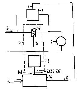
Accordlng to FIG. 1, a load, for example a motor Z,
ls connected vla a semlconductor valve 4, for example a trlac
or a clrcult conslstlng of several semlconductor valves, such
as a thyrlstor clrcult arrangement, to the
20365-3109
2~46268
~. . .~ .
phase of a single-phase alternating system. The
semiconductor valve 4 is provided with a control
electrode 5 and is part of a firing device 10, which
contains an ignition amplifier 12, for example an opto-
triac or an ignition transformer, that is required foroperating the semiconductor valve 4. An optically fired
semiconductor valve can also be provided in place of an
electrically fired semiconductor valve.
The open-loop control of the semiconductor valve 4
takes place through phase-angle or ignition-phase
control. To this end, in dependence upon the phase
relation, a firing signal that causes the semiconductor
valve 4 to be fired, is applied to the control electrode
5.
In the preferred specific embodiment according to
the FIG. 1, a reference detector 6 is assigned to the
semiconductor valve 4. This reference detector 6
determines, for example, the current zero crossing of
the current I flowing in the electric circuit as a
function of the voltage drop across the semiconductor
valve 4. The current zero crossing is used to establish
a time reference for the phase-angle control. A
corresponding reference signal X is made available at
the output 8 of the reference detector 6. For this
purpose, the reference detector 6 contains, for example,
a comparator, which compares the absolute value of the
voltage drop across the semiconductor valve 4 to a
defined threshold value.
Thus, a reference signal X with two levels is
applied to the output 8. One level is a state that
indicates that a current is flowing in the phase. If
this current is smaller than a limiting current value
that corresponds to the threshold voltage value the
second state for the reference signal is provided. By
properly selecting a low value for this threshold, for
example about 10 V, this level essentially corresponds
then to zero current and the reference signal X
~4~21i8
~.
essentially reproduces the circuit states of the
semiconductor valve 4. The edges between these two
circuit states then coincide in time at least roughly
with the current zero crossing of the current I flowing
through the semiconductor valve 4.
To establish a time reference for the phase-angle
control, one can also draw upon another characteristic
parameter in the current's time slope, for example the
maximum or minimum, or upon a characteristic parameter
in the time slope of the voltage.
The output 8 of the reference detector 6 is
connected to a forward controlling element 14, which
shunts off a time-delayed firing signal Z and holds it
ready at a control output 141. This firing signal Z is
either a safety firing signal ZS derived from the
preceding firing signal Z or a firing signal ZX derived
from the reference signal X and time-delayed in
accordance with a specified firing angle.
The firing angle is defined by the forward
controlling element 14, for example within the scope of
a control program that can be selected externally, as
well as within the scope of motor parameters that can be
input externally. It is also possible for the firing
angle to be time-dependent through a program that runs
internally in the forward controlling element 14. Thus,
for example, the motor 2 is able to start smoothly as
the result of a time-dependent firing angle, which
starting from a specified starting value is reduced to a
minimal value.
In FIG. 2, the current I flowing through the
semiconductor valve and, in FIG. 3, the voltage drop VT
existing across the semiconductor valve, are plotted
over time. When the current is extinguished at the
instant Tl, the voltage drop increases and, due to the
inductive reaction of the rotating motor, at a later
instant, T2, attains the threshold value -L required to
switch the comparator that follows. The comparator
2Ql~6268
configured in the reference detector 6 then switches, in
accordance with FIG. 4, from a signal level 30 to a
signal level 32.
These two signal levels 30 and 32 correspond to two
logic states, which indicate whether the voltage drop
across the semiconductor valve is smaller or greater in
value than the threshold value L. The signal levels 30
and 32 are separated from each other by a first, in the
example of the figure, falling edge 34 and a second, in
the example of the figure, rising edge 36. In the ideal
case, these edges correspond to the instant the current
zero point is reached and the firing instant
respectively.
Starting from the edge 34, the forward controlling
element 14 generates a firing signal Z at the instant T2
+ DT. This firing signal Z is delayed by the delay time
DT and results in the current being re-ignited at the
instant T3. The firing signal Z is generated by the
reference signal X and therefore, in addition,
designated as ZX in FIG. 5.
At the instant T4, the current is once more
extinguished and the voltage drop VT across the
semiconductor valve rises. However, in the example of
FIG. 3, it does not attain the threshold value +L, which
is required to generate an edge 34 for the reference
signal X. This can be the case, for example, when the
motor is underloaded for the short term and the voltages
induced in the motor windings when the motor continues
to run prevent the voltage drop VT across the
semiconductor valve from being large enough to attain
the threshold value +L required for switching. In this
case, at the instant T5, the forward controlling element
makes available a safety firing signal ZS, which is
delayed with respect to the preceding firing signal Z by
an absolute or preset time interval P and causes the
current to be fired at the instant T6. This time
interval P corresponds to an angular distance, which is
~0~6268
'_
preferably greater than 175 and smaller than 185, in
particular about 18a.
At the instant T7, the current is once again
extinguished and, in the example of FIG. 3, a voltage
drop is generated across the semiconductor valve and, at
the instant T8, reaches the threshold value -L required
to switch the comparator. After a time delay DT, a
firing signal Z is generated, which causes the current
to be re-ignited at the instant T9. This firing signal,
in turn, is generated by the reference signal X and is
therefore likewise designated as ZX in FIG. 5.
A safety firing signal ZS' is likewise drawn with a
dotted line in FIG. 5. This safety firing signal ZS'
would then be applied when no reference signal X is
transmitted within the time interval T5 + P by the
reference detector to the forward controlling element.
In the example of FIG. 5, a time interval P2 for the
safety firing signal ZS' is also drawn in. It
corresponds to the time interval P1 between the firing
signal ZX and the safety firing signal ZS. According to
an advantageous modification, for example, the danger of
continuously firing with the same small firing angle
differential can be avoided by having variable time
intervals Pl and P2. In this case, it is particularly
advantageous for P1 to correspond to an angular distance
of 18~ + D and P2 to an angular distance of 18~ - D.
Here, D preferably amounts to about 5, so that generally
the relationship
P2n~1 . f . 36~ = 18a + D and P2n . f . 36~ = 18~ - D
is satisfied, whereby the running index represents the
number of safety firing signals in series that are not
triggered by a reference signal. This guarantees that
the phase error is still limited even when safety firing
signals occur repeatedly in series.
2046268
In an advantageous specific embodiment according to
FIG. 6, the forward controlling element comprises a
control unit 16, which is connected to the reference
detector. The control unit 16 is connected to a free-
running counter 22 and reads the counter reading at aninstant that is specified by the reference signal X, for
example, by means of its falling edge. This value is
stored in a register 20 that is connected to the control
unit 16. The counter 22 and the register 20 are
connected to a comparator unit 18, which continually
compares the reading of counter 22 to the reading of
register 20 and, when there is conformity, causes the
control unit 16 to apply a firing signal.
In a preferred specific embodiment, the forward
controlling element 14 comprises a microprocessor, in
which three asynchronous processes are provided. They
are illustrated on the basis of the flow charts of FIG.
7. In a first process, the system waits for a reference
signal X to appear and then, for example, when a falling
edge 34 appears, a preset delay time DT is added to the
current reading TI of the free-running counter 22 and
recorded in the register 20. Moreover, a further
process is provided, which reads out the current reading
TI of the free-running counter 22 when a firing signal Z
appears, for example at the rising edge of the firing
signal Z, adds a specified value P to it, and likewise
stores the sum in register 20. A further process tests,
if the reading TI of the free-running counter 22 is
greater or equal to the reading T of register 20. If
this is the case, then a firing signal Z is applied.
The present invention is clarified for single-phase
A.C. power controllers on the basis of FIGS. 1 through
7. The same considerations also apply, however, for
each phase of a multiphase A.C. power controller.