Note: Descriptions are shown in the official language in which they were submitted.
1
E~H 158 CA
July 16, 1991
Arrangement far Processing Sensor Signals
The invention consists in an arrangement for processing sensor
signals furnished by a capacitive sensor which includes a
measuring capacitance influenceable by a physical measured
quantity to be determined and at least one refer'snce capacitor
having a reference capacitance infl.u~nceable in another manner
and furnishing a measuring effect dependent on_said measuring
capacitance and said reference capacitance, comprising a signal
processing circuit which operates by the principle of quantized
charge transport by means of switch-capacitor structures and
charge balancing at least in time average and which receives
said sensor signals representing said measuring effect and
furnishes an output signal corresponding to said measuring
effect, wherein first electrodes of said capacitors of said
sensor lie at a fixed potential and second electrodes of them
for performing said charge transport are connectable to a first
input of an input operational amplifier, a second input of
which lies at a reference potential, and wherein a reverse
charging of said capacitors of said sensor necessary for
forming transported charge packets is effected by switching
over said reference potential of said input operational
amplifier.
In the periodical "IEEE Transactions on Instrumentation and
Measurement", Dec. 1987, pp. 873 to 878, an arrangement for
processing sensor signals furnished by a capacitive sensor is
described which includes a measuring capacitance influenceable
z~~s~~~
by a physical measured quantity to be determined and at least
one reference capacitor having a reference capacitance
influenceable in another manner and furnishing a measuring
effect dependent on said measuring capacitance and said
reference capacitance, comprising a signal processing circuit
which operates by the principle of quantized charge transport
by means of switch-capacitor structures and charge balancing at
least in time average and which receives said sensor signals
representing said measuring effect and furnishes an output
signal corresponding to said measuring effect.
Signal processing by the principle of quantized charge
transport by means of switch-capacitor structures and charge
balancing has the advantages that offset voltages of the
operational amplifiers used have no influence on the output
signal, that the circuits are completely integrable in CMOS
technology and that no accurate long-term reference voltage is
necessary. Furthermore, from the clock pulses with which the
switch-capacitor structures are controlled for performing the
charge transports two clock signals can be derived, the
frequency or pulse ratio of which is directly proportional to
the measuring effect so that the measurement result is
available in digital form.
In this pre-described circuit, one electrode of each of the
capacitors of the sensor or an electrode common to them is
connected by the signal line leading to the signal processing
circuit to an input of an operational amplifier, the other
input of which lies at a fixed reference potential, for example
ground potential. By periodically actuated switches the
voltages which are necessary for reverse charging in order to
produce the charge packets to be transported, are applied to
the other electrodes of the sensor capacitors.
3
A disadvantage of this pre-described arrangement is that all
said electrodes are active. The function can, therefore, be
disturbed if charges are coupled onto the electrodes connected
to the signal line by external electric fields. Shieldings
necessary to suppress such charge couplings restrict the
construction and use possibilities and consequently cannot
always be applied.
An object of the invention is to provide an arrangement which
whilst retaining the advantages of the signal processing by the
principle of quantized charge transport by means of switch-
capacitor structures and charge balancing permits a one-sided
fixed connection of said capacitors to any desired potential.
In the arrangement according to the invention use is made of
the fact that the two inputs of an operational amplifier,
except for the offset voltage, lie virtually at the same
potential. By switching over the reference potential of the
input operational amplifier the potential of the respective
capacitor electrode connected to the other input is therefore
changed in the same manner. In this way the voltage changes
necessary for reverse charging of the sensor capacitors can be
executed at the capacitor electrodes connected to the signal
line so that only said electrodes are active. In contrast, the
other electrodes, which are always inactive, can be applied to
any desired potential which may for example be the housing
potential of a corresponding sensor. The only condition for
this potential is that it must be stable in the short-time
range relatively to the supply signal used for the signal
processing.
Advantageous embodiments of further developments of the
invention are characterized in the subsidiary claims.
4
Further features and advantages of the invention will be
apparent from the following description of examples of
embodiment which are illustrated in the Figures of the drawing.
Fig. 1 shows a fundamental scheme for explaining the problem
underlying the invention,
Fig. 2 shows a sectional view of a capacitive sensor,
Fig. 3 shows the circuit diagram of a first embodiment of a
signal processing circuit working with quantized
charge transport by means of switch-capacitor
structures and charge balancing and furnishing a
frequency as output signal,
Fig. 4 shows time diacjramms of signals occuring in the signal
processing circuit of Fig. 3 during its operation,
Fig. 5 shows the circuit diagram of a second embodiment of a
signal processing circuit working with quantized
charge transport by means of switch-capacitor
structures and charge balancing and furnishing an
analog output signal, and
Fig. 6 shows time diagramms of signals occuring in the signal
processing circuit of Fig. 5 during its operation.
~fl~~~3t~~
(o improve understanding, in Fig. 1 the principle of the
processing of sensor signals on which the invention is based
is shown. Fig. 1 shows a capacitive sensor 1 with the aid of
which a physical quantity G is to be measured and a signal
processing circuit 2 connected to the sensor 1. The sensor 1
contains a measuring capacitor the capacity of which is
variable in dependence upon the physical quantity to be
measured. A supply signal source 3 furnishes to the sensor 1 a
supply signal V which makes it possible to convert the change
of the measuring capacitance to an electrical sensor signal
which is supplied to the signal processing circuit 2 and
expresses the measuring effect M representing the relationship
of the physical quantity G to be measured and the measuring
capacitance. The signal processing circuit 2 converts the
sensor signal to an output signal S of the desired form which
is preferably related to a reference signal Sref' Depending on
the construction of the signal processing circuit 2, the output
signal S may for example be an analog signal, a digital signal
or a frequency.
If it is assumed for example that the physical quantity G to
be measured is a pressure the capacitive pressure sensor 10
illustrated in sectional view in Fig. 2 may be used for the
sensor 1. The pressure sensor 10 has a base body 11 and a
diaphragm 12 which are connected together at the periphery by
a spacer ring 13. The face of the diaphragm 12 facing the base
body 11 is provided with a metallization 14 which is connected
to a connection conductor 15 led through the spacer ring 13
and the base body 11. The face of the base body 11 facing the
diaphragm 12 carries a central circular metallization 16 which
is connected to a connection conductor 17 led through the base
body 11 and an annular metallization 18 surrounding the
metallization 16 and connected to a connection or terminal
conductor 19 led through the base body 11.
2~~~~r~~
6
When a pressure P acts on the outer surface of the diaphragm
12 the latter is deformed so that the distance between the
centre region of the metallization 14 and the opposite central
metallization 16 varies in dependence upon said prossure. The
two metallizations 14 and 16 therefore form the electrades of
a measuring capacitor having a capacitance Cx which depends on
the pressure P and can be measured between the connection
conductors 15 and 17. In contrast, the distance between the
edge region of the metallization 14 and the opposite annular
electrode 18 remains substantially unchanged during the
pressure-dependent deformation of the diaphragm 12 because
said distance is fixed by the spacer ring 13. The two
metallizations 14 and 18 therefore form the electrode of a
reference capacitor having a capacitance Cref which is
independent of the pressure P and can be measured between the
connection conductors 15 and 19.
The measuring effect M dependent on the pressure and used in
the signal processing circuit 2 for generating the output
signal S/Sref is therefore in such a capacitive pressure
sensor the change of the measuring capacitance Cx relatively
to the reference capacitance Cref' Depending on the particular
use, the measuring effect can be differently represented. For
example, the measuring effect M1 can correspond to the
capacitance ratio Cx/Cref between the measuring capacitance
and the reference capacitance but preferably the capacitance
ratio (Cx - Cref~~Cref is used because by forming the
difference larger relative changes are obtained. A further
possibility would be the capacitance ratio (Cx - Cref~/Cx' Df
course, the pressure-dependent measuring capacitance Cx may be
used as measuring effect on its own but the quotient formation
has the advantage that the measuring effect remains largely
unaffected by disturbing influences acting in the same manner
on the two capacitances Cx and Cref'
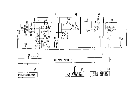
Fig, 3 shows an example of embodiment of the signal processing
circuit of Fig. 1 for the signal processing of the sensor
signal furnished by a capacitive sensor 20. The sensor 20
includes a measuring capacitor 21 of capacitance Cx and a
reference capacitor 22 of capacitance Cref. An electrode.24 is
common to the measuring capacitor 21 and the reference
capacitor 22. The measuring capacitor 21 is formed by an
electrode 26 cooperating with the common electrode 24 and the
reference capacitor 22 is formed by an electrode 28 cooperating
with the common electrode 24. The capacitive sensor 20 may for
example have the structure illustrated in Fig. 2, the electrodes
24, 26, 28 of Fig. 3 then corresponding to the metallizations
14, 16 and 18 respectively of Fig. 2. The measuring effect M
of interest is the capacitance ratio (Cx - Cref,~Cref'
The common electrode 24 is connected via its connection
conductor 25, corresponding to the connection conductor 15 of
Fig. 2, to a fixed potential which may for example be the housing
potential of the sensor 20. The sensor 20 is thus potential-
bound on one side. In Fig. 3 the potential at the connection
conductor 25 differs by a fixed voltage U1 from the potential
of a reference conductor 30; the voltage U1 corresponds to the
supply signal V of Fig. 1.
The electrodes 26, 28 are connected via shielded signal lines
27, 29 corresponding to the connection conductors 17 and 19 of
Fig. 2 to a function block 31 of the signal processing circuit.
The function block 31 contains two switch groups 32 and 33.
The function block further includes a voltage divider 34
having three series-connected resistors 35, 36, 37 to which
the voltage U1 existing between the connection conductor 25
and the reference conductor 30 is applied. The voltage divider
34 has a first tap 38 between the resistors 35 and 36 and a
second tap 39 between the resistors 36 and 37. When the
voltage U1 is present at the voltage divider 34 the voltage U2
is present between the tap 38 and the reference conductor 30
and the voltage U3 between the tap 39 and the reference
conductor 30.
~0~~~~~~:
8
The function block 31 is followed by a buffer 40 including an
operational amplifier A1, a storage capacitor 41 of capacitance
Cs and two switches S1 and S2. When the switch S1 is closed it
connects the output of the operational amplifier A1 to the
noninverting input thereof. When the switch S2 is closed it
connects the output of the operational amplifier A1 to the one
electrode of the storage capacitor 41, the other electrode of
which is connected to the inverting input of the operational
amplifier A1 so that the storage capacitor 41 then lies in the
feedback circuit of the operational amplifier A1. The reference
potential of the operational amplifier A1 present at the non-
inverting input differs from the potential of the reference
conductor 30 by a voltage U4. The potential at the inverting
input differs from the reference potential of the noninverting
input by the offset voltage U01 of the operational amplifier
A1. .
Between the inverting input of the operational amplifier A1
and the reference conductor 30 there is a parasitic capacitance
Cp represented in Fig. 3 by a capacitor symbol.
The switch group 32 includes four switches S3, S4, S5. S6~
When the switch S3 is closed it connects the electrode 26 of
the measuring capacitor 21 to the inverting input of the
operational amplifier A1 and when the switch S4 is closed it
connects the electrode 26 of the measuring capacitor 21 to the
reference potential at the noninverting input of the
operational amplifier A1. When the switch S5 is closed it
connects the electrode 28 of the reference capacitor 22 to the
inverting input of the operational amplifier A1 and when the
switch S6 is closed it applies the electrode 28 of the
reference capacitor 22 to the reference potential at the
noninverting input of the operational amplifier A1.
9
The switch group 33 contains two switches S~ and S8. When the
switch S~ is closed it connects the noninverting input of the
operational amplifier A1 to the tap 38 of the voltage divider
34 so that the voltage U4 present at the noninverting input of
the operational amplifier A1 is formed by the voltage U2. When
the switch S8 is closed it connects the noninverting input of
the operational amplifier Al to the tap 39 of the voltage
divider so that the voltage U4 present at the noninverting
input of the operational amplifier A1 is formed by the voltage
U3.
The buffer 40 is followed by an integrator 42. The integrator
42 includes an operational amplifier A2, an integration
capacitor 43 of capacitance C1 lying in the feedback circuit
of the operational amplifier A2 and a switch S9. When the
switch S9 is closed it connects the inverting input of the
operational amplifier A2 to the storage capacitor 41 in the
buffer 40. The noninverting input of the operational amplifier
A2 is applied to ground.
The potential at the inverting input differs from the ground
potential of the noninverting input by the offset voltage U02
of the operational amplifier A2. Between the output of the
operational amplifier A2 and the reference conductor 30 the
output voltage UA2 appears.
A comparator 45 following the integrator 42 includes an
operational amplifier A3 which is connected in known manner as
threshold value comparator in that its feedback circuit is
open. The inverting input of the operational amplifier A3 is
connected to the output of the operational amplifier A2 in
the integrator 42 and a threshold voltage US is applied to the
noninverting input of the operational amplifier A3 with
respect to the reference conductor 30. The offset voltage U03
is present between the two inputs of the operational amplifier
A3. In accordance with the known function of such a threshold
i
value comparator the output voltage UA3 of the operational
amplifier A3 has a low value when the voltage UA2 lies above
the threshold voltage US and it assumos a high value when the
voltage UA2 drops below the threshold voltage US.
The switches S1 to S9 are actuated by control signals. which
are furnished by a control circuit 46 which is synchronized by
a clock signal furnished by a clock generator 47. For
simplification, the control signals are denoted by the same
reference numerals S1, S2, ... S9 as the switches controlled
by them. The time profile of the control signals is shown in
the diagrams of Fig. 4. Each switch Si, S2 ... S9 is open when
the signal controlling it has the low signal value and is
closed when the signal controlling it has the_high signal
value.
The switches S1, S2 ... S9 are represented symbolically as
mechanical switch contacts but in reality of course they are
highspeed electronic switches, for example field-effect
transistors.
The control circuit 46 has a control input which is connected
to the output of the operational ampl~.fier A3 in the comparator
45. Furthermore, the control circuit 46 has an output to which
a measuring cycle counter 48 is connected and a further output
to which a compensation cycle counter 49 is connected.
The circuit illustrated in Fig. 3 operates on the principle of
charge balancing. In consecutive cycles, controlled by the
switches S1 to S8 charge packets are applied to the capacitors
21 and 22 of the sensor 20, said packets depending on the
voltages U2, U3 a.nd on the capacitances Cx, Cref of said
capacitors. The maximum magnitude of the charge packets within
the circuit for given capacitance values of the sensor 20 is
defined by the voltage divider 34. The charge packets are
buffered in the storage capacitor 41 and by closing of the
~o4s~~~~
11
switch S9 transferred to the integration capacitor 43 in which
they are summated. The voltage UA2 corresponds to the voltage
at the integration capacitor 43 which in turn depends on the
charge integrated on the integration capacitor. The sequence
of the circuit is controlled so that for Cx > Cref the voltage
UA2 becomes progressively smaller. If the voltage UA2 drops
below the predetermined threshold voltage US of the comparator
45 the output voltage UA3 of the latter flips to its maximum
value, the control circuit 46 thereby being caused to perform
a compensation cycle. In the compensation cycle the switches
S1 to S8 are controlled in such a manner that on the next
closing of the switch S9 a compensation packet is transferred
to the integration capacitor 43 which is substantially
proportional to the capacitance Cref of the reference
capacitor 22 with a sign such that the voltage UA2 is again
raised above the threshold voltage US. As a result, charge
balancing takes place in the integration capacitor 43 because
on a time average the sum of all the integrated charge packets
is equal to zero. This equilibrium is always present at the
instants in which the voltage UA2 drops below the threshold
voltage US of the comparator 45.
The sequence of the function described generally above will
now be explained in detail with the aid of the diagrams of
Fig. 4. Apart from the already mentioned time profile of the
switch control signals S1 to Sg the diagrams of Fig. 4 also
show the time profile of the voltages U4, UA2 and UA3 and of
the voltage Ups at the storage capacitor 41 in several cycles,
one of which is a compensation cycle K. The other cycles,
which are not compensation cycles, are referred to as measuring
cycles M. Each cycle consists of six phases numbered 1 to 6.
The switches S1 and S2 are controlled by a periodic square-
wave signal in antiphase relationship so that the switch S1 is
open when the switch S2 is closed and vice-versa. In each
2~4~~~~
12
cycle the switch S1 is closed during the phases 1-2 and 4-5
and open during the phases 3 and 6. When the switch S1 is
closed and the switch S2 is open the capacitors 21 and 22 of
the sensor 20 lying in the input circuit of the operational
amplifier A1 can be connected by the switches S3 and S5,
respectively, to the voltage present at the inverting input of
the operational amplifier A1 and correspondingly charged
without thereby influencing the charge in the storage
capacitor 41. This state is referred to as "conditioning
phase".
The switches S7 and S8 are likewise controlled by a periodic
square-wave signal in antiphase relationship so that the
switch S7 is open when the switch S8 is closed and vice-versa.
When the switch S7 is closed and the switch S8 is open the
voltage U4 is equal to the voltage U2; when the switch S~ is
closed and the switch S7 is open the voltage U4 is equal to
the voltage U3. Thereat U2 > U3. The measuring and compensation
charge packets are generated substantially by these abrupt
changes in the voltage U4.
The switch Ss is actuated in each case synchronously with the
switch S3 and the switch S4 is actuated synchronously with the
switch S5, except for the compensation cycles. The purpose of
the switches S4 and Ss is to apply the respective inactive
signal line 27 or 29 of the sensor 20 to a potential which
differs from the potential of the active signal line only by
the offset voltage U01 of the operational amplifier A1. As a
result, the coupling of erroneous charges via the respective
inactive sensor capacitor 21 or 22 and the signal line 27 or
29 thereof to the active signal line is avoided. This function
is presumed in the following description; the respective
positions of the switches S4 and S6 will therefore not be
separately mentioned.
Hereinafter the time sequence of the operation of the signal
processing circuit will be described first for a measuring
cycle M and then for a compensation cycle K.
20~~~t~j~
1. Measuring cycle M
Phase 1:
At the start of phase 1 of each measuring cycle M the charge
applied in the preceding cycle is still present on the storage
capacitors. The switches S1 and SS are closed whilst at the
same time the switch S2 is opened. As a result the storage
capacitor is separated from the output of the operational
amplifier A1 and connected to the input of the integrator 42
so that a charge transfer takes place from the storage
capacitor 41 to the integration capacitor 43. Furthermore, in
phase 1 the switch S~ is open and the switch S8 closed so that
the voltage U4 at the noninverting input of the operational
amplifier A1 is formed by the voltage U3. After the discharge
of the storage capacitor 41 the impressed voltage
UCs - U02 U3 U01 (1)
is present at said storage capacitor 41. Thus, on the storage
capacitor 41 there is the residual charge
QCs(R) - (U02 U3 U01) ~ Cs (2)
The reverse charge amount flows to the integration capacitor
43. In all further phases 2 to 5 of each cycle the switch S9
is open so that in these phases no reverse charging can take
place from the storage capacitor 41 to the integration
capacitor 43.
Furthermore, in phase 1 the switch S3 is closed so that the
measuring capacitor 21 is connected to the inverting input
of the operational amplifier A1. Since at the same time the
switch S1 is closed and the switch S2 open, the circuit is in
the conditioning phase for the measuring capacitor 21. The
measuring capacitor 21 is charged with U4 = U3 to the charge
QCx(1) _ (U01 + U3 _ U1) (3)
(conditioned) without thereby influencing the charge on the
storage capacitor 41.
Phase 2:
In phase 2 the switch S3 is opened whilst the switch S5
remains open so that the two capacitors 21 and 22 of the
sensor 20 are separated from the inputs of the operational
amplifier A1. At the same time the switch S~ is closed and the
switch S8 opened so that the voltage U4 jumps from the value
U3 to the value U2. The parasitic capacitance Cp is
correspondingly reverse charged. Since the swatch S1 is still
closed and the switch S2 open, the entire charge necessary for
reverse charging the parasitic capacitance Cp is furnished by
the output of the operational amplifier A1. The charges on the
storage capacitor 41 and on the integration capacitor 43
remain uninfluenced by this reverse charging.
Phase 3:
In phase 3 the switch S1 is open and the switch S2 closed so
that the buffer 40 is ready for the transfer of charge to the
storage capacitor 41. At the same time the switch S3 is closed
again so that the measuring capacitor 21 is connected to the
inverting input of the operational amplifier A1 and reverse
charged to the charge
qCx(3) _ (U01 + U2 - U1) (4)
The reverse charge amount
dQCx (3) = QCx (3) QCx (1) - (U2 U3) ~ Cx ( 5)
flows to the storage capacitor 41.
2~~~~~~
Phase 4:
Phase 4 is the conditioning phase for the reference capacitor
22 because the switch S1 is closed and the switch S2 is open
and at the same time the switch S5 is closed so that the
reference capacitor 22 is connected to the inverting input of
the operational amplifier A1. Since the switch S~ is still
closed and the switch S8 open, the voltage U4 has the value
U2. The reference capacitor 22 is thus charged (conditioned)
to the charge
OCref(4) - (U01 + U2 U1) ~ Cref
without the charge on the storage capacitor 41 being influenced
thereby.
Phase 5:
The switch S5 is opened so that the reference capacitor 22 is
separated from the inverting input of the operational
amplifier A1. The switch S~ is opened and the switch S8 closed
so that the voltage U4 jumps from the value U2 to the value U3
and the parasitic capacitance Cp is correspondingly reverse
charged. Since the switch S1 is still closed and the switch
S2 open, the entire charge necessary for reverse charging the
parasitic capacitance Cp is furnished by the output of the
operational amplifier A1 without the charges on the storage
capacitor 41 and on the integration capacitor 43 being
influenced thereby.
Phase 6:
In phase 6 the switch S1 is open and the switch S2 closed so
that the buffer 40 is ready for the transfer of charge to the
storage capacitor 41. At the same time the switch S5 is again
closed so that the reference capacitor 22 is connected to the
inverting input of the operational amplifier A1 and is reverse
charged to the charge
16
aCref(6) - (U01 ~ U3 U1)
The reverse charge amount
dQCref (6) - QCref (6) aCref (4) - (U2 U3) ~ Cref
flows to the storage capacitor 41.
This completes the measuring cycle M. At the end of the
measuring cycle M the storage capacitor 41 contains the
resultant charge
QCs = QCs(R) + dQCx(3) + dWCref(6) (9)
- qCs (R) + (U2 U3) ~ (Cx Cref)
In phase 1 of the following cycle the storage capacitor 41 is
again discharged to the residual charge WCs(R) according to
the equation (2), the reverse charge amount
dQM = QCs(R) qCs - (U2 U3)~ (Cx Cref) (10)
being transferred to the integration capacitor 43. The reverse
charge amount dQM is referred to as measuring charge packet.
With Cx > Cref and U2 > U3, the measuring charge packet dQM is
negative so that is causes a negative voltage jump in the
voltage UA2.
The phases 1 to 6 of each measuring cycle M are cyclically
repeated until the voltage UAZ drops below the threshold
voltage US of the comparator 45 and the level of the voltage
UA3 changes from a low to a high value. The control circuit 46
is thereby caused to perform a compensation cycle K.
~O~b~~~~
2. Compensation cycle K
The sequence for a compensation cycle K is identical to the
sequence of the measuring cycles M except for the difference
that~the switch S3 remains open and the switch S4 remains
closed all the time. As a result, during the entire
compensation cycle K no charge flows from the measuring
capacitor 22 into the storage capacitor 41. Accordingly,
instead of equation (5) we have
dQCx(3) - ~ (11)
if equations (11) and (8) are inserted into equation (9), this
gives as resultant charge in the storage capacitor 41 at the
end of the compensation cycle K:
QCs - QCs(R) + dQCx(3) + dQCref(6) (12)
- QCs(R) (U2 - U3) ~ Cref
In phase 1 of the following cycle the storage capacitor 41 is
again discharged to the residual charge QCs(R) according to
equation (2), the reverse charge amount
dQK - QCs (R) QCs - fi(U2 U3) ~ Cref (13)
being transferred to the integration capacitor 43. The reverse
charge amount dQK is referred to as compensation charge
packet. With U2 > U3 the compensation charge packet dQK is
positive so that it causes a positive voltage jump in the
voltage UA2. The positive voltage jump results in the voltage
UA2 again being raised above the threshold voltage US so that
the level of the voltage UA3 again goes from the high value to
the low value. This causes the control circuit 46 to perform
measuring cycles M again, the compensation cycle K thereby
being completed.
20463~~~
Charge balance
Equations (10) and (13) describe the measuring charge packets
dQM and the compensation charge packets dQK respectively. The
measuring method operates by the process of charge balancing,
i.e. a charge equilibrium arises in the integration capacitor
43. The charge equilibrium in a time average is always present
at the instants when the voltage drops below the threshold
voltage US. If the charge state of the integration capacitor
43 is considered, then a predetermined number of measuring
charge packets dQM is integrated until the voltage drops below
the threshold voltage US; the integrated measuring charge
packets are then compensated by a compensation charge packet
dQK and the process starts again.
On each execution of a measuring cycle M the control circuit
46 supplies a pulse to the counting input of the measuring
cycle counter 48 and on each execution of a compensation cycle
a pulse to the counting input of the compensation cycle
counter 49. If a time interval in which the measuring cycle
counter 48 has counted a..~total of n measuring cycles M and the
compensation cycle counter 49 a total of k compensation cycles
K is considered, due to the charge balancing the following
must be true:
n~dQM + k~dQK = 0 (14)
-n' (UZ - U3) ~ (Cx Cref) + k~ (U2 - U3) ' Cref = 0 (15)
Thus, the desired capacitance ratio is obtained directly from
the ratio of the pulses counted in the counters 48 and 49 in
the time interval considered:
k Cx ~ Cref
a _ (16)
n Cref
20463~~4
19
The same result is obtained if the ratio of the repetition
frequencies of the pulse trains supplied to the two counters 48
and 49 is formed.
The capacitance values of the capacitors 41 and 43, the offset
voltages of the operational amplifiers, the reference potential
U1 of the sensor 20, the operating voltage of the circuit and
the frequency with which the control circuit 46 is clocked, do
not enter into the measurement result, as is apparent from
equation (16).
The value of the voltage U1 is limited only by the working
range of the circuit.
In Fig. 3 the shields of the signal lines 27 and 29 are
connected to the line leading from the switch group 33 to the
noninverting input of the operational amplifier A1. The
potential of the shields is thereby made to follow up the
changing reference potential of the input operational
amplifier and thus always substantially corresponds to the
potential of the shielded conductors. This step also
contributes to avoiding error charges being coupled onto the
active signal line.
Fig. 5 shows a second embodiment of the signal processing
circuit 2 according to Fig. 1 for the signal processing of the
sensor signal furnished by the capacitive sensor 20. The signal
processing circuit according to Fig. 5 differs from that of
Fig. 3 by the following features: The comparator 45 and the
counters 48, 49 are not present, but the other circuit parts of
Fig. 3 bearing the same reference numerals are present. A
further difference consists in the presence of a third switch
group 50 consisting of the switches S10, S11-
~~L.~~~3~~.~
The terminal of the voltage divider 34 not facing the reference
conductor 30 is connected either via the switch S10 to the
output of the integrator 42 or via the switch S11 to the
connection conductor 25. The switches S11, S12 the control
signals of which are also generated by the control circuit 46
are never closed at the same time. Furthermore, they are open -
lii;,e the switches 51...59 - when the control signal has its low
level and they are closed when the control signal has its high
level. Again the control signals of the switches 511, S12 are
denoted by the same reference numerals as the switches
themselves. They are realized by means of fast electronic
switches as already mentioned above.
The circuit of Fig. 5 operates like that of Fig. 3 according to
the principle of charge balance. Again controlled by the
switches S1...S8 charge packets are transferred to the
capacitors 21, 22 of the sensor 20 during consecuting cycles.
The charge packets are depending on the voltages U1, U3 and on
the capacitances Cx, Cref of these capacitors. The maximum
value of the charge packets of a given circuit and given capac-
itances of the sensor 20 is defined by the voltage divider 34.
The charge packets are buffered in the storage capacitor 41 and
by closing of the switch S9 transferred to the integration
capacitor 43 in which they are summated. The voltage UA2
corresponds to the voltage at the integration capacitor 43
which in turn depends on the charge integrated thereon.
The sequence of the common function of Fig. 5 just described
will now be explained only so far as it deviates from the
function of Fig. 3 and its diagramms of Fig. 4. Apart from the
time profile of the switch control signals Sl...sll the Fig. 6
shows also the time profile of the voltages U4, UA2 and of the
voltage UCs at the storage capacitor 41 in several cycles, each
second of which is a compensation cycle K. The other cycles,
which are not compensation cycles, are again referred to
2040~1~~
21
measuring cycles M. The alternate sequence of the cycle types
of Fig. 6 is only an example; an optional number of compens-
ation cycles can rather follow to an optional number of
measuring cycles. Each cycle consists of six phases numbered
again by 1 to 6.
Controlling of the switches S1...S8 and the functions thereby
generated are equal to those of the switches 51...58 of Fig.3.
In contrary to Fig. 3 the switch S9 is open during each com-
pensation cycle. Therefore, charge is transferred to the
integration capacitor 43 only during phase 1 of the measuring
cycles M.
Furthermore, switch S11 is closed during the measuring cycles M
as well as during phase 1 of the compensation cycles. There-
fore, at these moments the terminal of the voltage divider 34
not facing the reference conductor 30 lies at the connection
conductor 25 and at the fixed voltage U1.
In this phase the following equation holds:
U2 U3 - U1~R36~~R35 + R36 + R37~ Ul~vR (17)
In the phases 2 to 6 of the compensation cycles K switch S11 is
open and switch S10 is closed. Therefore, the voltage divi-
der 34 is connected to the output of the integrator 42 and the
analog output voltage UA2 of the operational amplifier A2 lies
at the voltage divider 34.
In these phases the following equation holds:
U2 - U3 - UA2~R36~~R35 + R36 + R37~ - UA2~vR ~18~
2U~6~~4
2z
The reference numerals R35, R36, R37 of equations (17), (18)
designate the resistances of the resistors 35, 36, 37 of the
voltage divider 34.
The equations (15), (16) holding for optional numbers n, k of
cycles change, therefore, to:
-n'U1°VR°(Cx Cref) + k~UA2~vR~Cref - 0 (19)
(kin)°(UA~~U1) ° (Cx - Cref)~Cref (20)