Note: Descriptions are shown in the official language in which they were submitted.
204677D ~:
.; -- 1 --
.
RD-19,669
~S~ " ';
Ei~l~ Qf the Inventio~ -
The present invention relates generally to power
supplies. More particularly, the present invention relates -
5 to a high-efficiency, high-density, power supply including a -~
dc-to-dc converter with an integral boost power supply for
maintaining the converter input voltage within its steady-
state range. ~ -
In an exemplary distributed power system, a single, ~ -
relatively high power supply converts input line voltage to a
semi-regulated voltage which is then supplied to a multitude
of individual "point-of-load" power supplies located at the
loads to be served. Power ls usually distributed to the
15 point-of-load supplies along the back-plane of a modular ~
assembly, and the relatively high power supply is thus often ~ -
referred to as a "back-plane" power ~upply. Typically, the
back-plane supply has its input derived from a prime power
source which may exhibit substantial voltage transients. The
back-plane supply must continuously supply the regulated
power to the point-of-load supplie~ despite these normal ~;
transient disturbances. In a military application of ;-
distributed power, for example, the prime power is often ~ -
specified to be that defined by military standard MIL-STD-
704D. The steady-state input voltage defined by this
standard is in the range from 250 to 280 Vdc. However, under
this standard, normal dc operation i~ defined as including an
envalope of voltage transients tha~ can make the effective
input voltage vary between 125 and 475 Vdc. Unfortunately,
however, high-frequency power supply topologies which meet
the aforementioned input voltage range requirement while
,'~: ,
.;:
2~77~
-- 2
RD-19,669
still maintaining high-efficiency, ste~dy-state operation
have been heretofore unavailable. In particular, as the
lower limit of the voltage range requirement decreases,
efficiency decreases. For example, in a resonant circuit
topology, which advantageously enables operation at high
frequencies and hence the use of small circuit components,
the decrease in efficiency is primarily due to the fact tha~
peak circulating currents in the resonant components and
primary-side active d~vices are determined by the minimum
voltage requirement. Since the peak circulating currents are
higher for a lower voltage requirement, an~ the circulating
currents remain relatively constant for voltages above the
minimum voltage requirement, conduction losses increase as
the minimum voltage requirement decreases. Alternatively, to
minimize losses, components can be made larger, but at the
expense of power densi~y. Therefore, it would be desirable
to provide a high-density po~er supply for supplying a
regulated output voltage at high ef~iciency even for an input
voltage which may exhibit substantial transients. To this
end, it would be desirable to employ a resonant converter
exhibiting substantially lossless switching, such as by the
zero~voltage switching technique described in "A Comparison
of Half-bridge Resonant Converter Topologies" by R.L.
Steigerwald, IEEE Transaction~ on Power Electronics, April
25 1988, pp. 174-182, which is hereby incorporated by reference,
while also providing means for minimizing active device
conduction losses, despite substantial input voltage
transients. ^;~
Accordingly, an object of the present invention is
to provide a new and improved high-efficiency, high-density
power supply suitable for use in a distributed power system.
. . ~
: ~ ~ . ' ; . ~ -
2~770
3 -
RD 19,669
Another object of the present invention is to
provide a power supply exhibiting relatively low active
device conduction losses as well as subs~antially zero
switching losses, even for an input voltage having a wide
voltage transient envelope.
Another object of the present invention is to
provide a high-efficiency, high-density, power supply
including a dc-to-dc converter and a boost power supply for
maintaining the effective input voltage to the converter
within a predetermined ~ange, even if the input voltage to
the power supply may exhibit substantial transients, so as to
avoid substantial active device conduction losses.
Still another object of the present invention is to
provide a high-efficiency, high-density power supply
including a dc-to-dc converter and an integral boost power
supply for maintaining the effective input voltage to the
converter within a predetermined range, such a power supply
being implemented with a minimal number of additional circuit
components.
The foregoing and other objects of the present
inven~ion are achieved in a power supply including a dc-to-dc ;
converter with an i~tegral boos~ power supply for maintaining
the effective converter input voltage within a predetermined
steady-state range, even if the input voltage to ~he power
supply exhibi~s ~ubstantial voltage transients. The boost
supply is coupled in series with the input voltage source and
is activated only during the input voltage transients.
According to a preferred embodiment, the boost power supply
comprises the secondary winding of a boost transformer and a
rectifier coupled in series wi~h two parallel-connected
converter modules. The converter module~ each comprise
either a half-bridge or a full-bridge connection of switching
',..
. ~ .
2~46~7~1
RD-19,669
devices. The primary winding of the boost transformer is
coupled between the junctions joining the switching devices
in each bridge converter module. In operation, the converter
modules are controlled by either pulse width modulation (PWM)
or resonant operation to generate a ~oltage across the
primary winding of the boost transformer.
In one preferred embodiment, each converter module
comprises a resonant converter including: two switching
devices connected in a half-bridge configuration, a resonant
circuit including an inductor and a capacitor coupled at the
junction between the switching devices, and an output voltage
rec~ifier. Alternatively, each converter module may comprise
a full-bxidge configuration of switching devices. The
primary winding of the boost transformer is coupled between
the junctions joining the switching devices of each converter
module. Resonant operation o~ the pair of converter modules
results in current sharing therebetween. Preferably, the
output voltage of the power supply is regulated by frequency
control, while the boos~ power supply is controlled using
phase-shift contxol o~ the resonant converter modules.
Moreover, if full-bridge converter modules are employed, the
power supply output voltage can be controlled using a
combination of frequency control and phase-shift control.
rief nescri~tiOn of th8 nraw m ~5
The features and advantages of the present
invention will become apparent from the following detailed
description of ~he invention when read with the accompanying
drawings in which:
Figure 1 is a partly schematic, block diagram of a
high-efficiency, high-density, power supply in accordance
with the present invention;
Figure 2 is a schematic illustration of a high-
efficiency, high-density, power supply employing half-bridge
,. , , ~- ,
.
:
2~77~
- 5 -
RD-19,669
resonant converter modules in accordance with one preferred
embodiment of the present invention;
Figure 3 graphically represents the output voltages
from the resonant converter modules and the voltage across
S the boost transformer for: (a) steady-state opera~ion .
wherein the boost power supply is inactive; and ~b~ transient
operation wherein the boost power supply generates a phase
shift between the output voltages of the resonant converter
modules in accordance with ~he present invention;
Figure 4 is a schematic illustration of a ~:
controller for controlling the operation of the po~er supply
of Figure 2 in accordance with a preferred embodiment of the
present invention; and
Figure 5 is a schematic illustration of a high-
efficiency, high-density, power supply employing full-bridge
resonant conver~er modules in accordance with an alternative !~'.:.~'.'
embodiment of the present invention. ~
~_ =~ , .
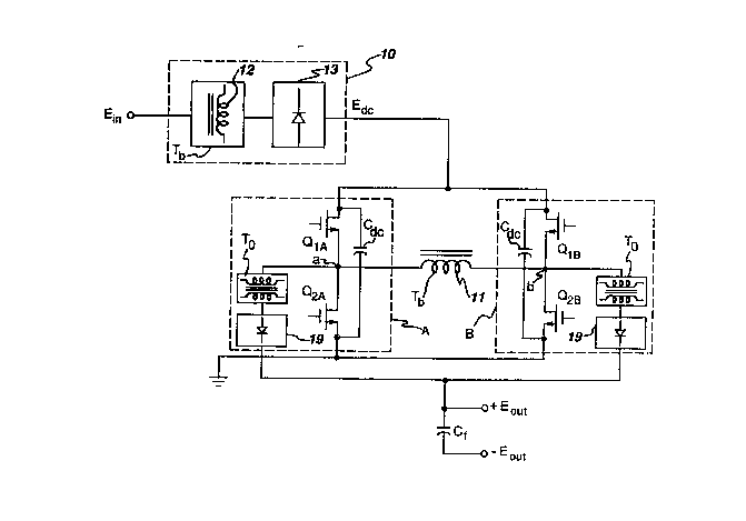
Figure 1 is a partly schematic, block diagram of a
20 high-efficiency, high-density, power supply in accordance :
with the present invention. Two parallel-coupled converter ::
modules A and ~ are connected in series with a boost power
supply 10. Each converter module comprises a half-bridge
connection of switching devices, a~ shown, although a full-
25 bridge connection may alternatively be employed. Moreover,
each conver~er module A and B may comp~ise either a resonant ~
converter or a PWM converter. In part~cular, although .
operation of resonant con~erter modules are described in ; .
detail hereinbelow to illustrate the principles of the
present invention, these principles are equally applicable to
PWM conver~ers, the operation of which i9 a matter well-known
to those of ordinary skill in the art. In Figure 1, for
purposes of illustration, each converter module is shown as
`: .' . ..
2~4~770
- 6
RD-19,669
comprising two switching devices Q1A-Q2A and Q1B-~2Br . .
respectively, connected in a half-bridge configuration with a
corresponding junction a and b, respectively, therebetween.
Switching devices Q1A~ Q2A~ Qla and Q2B ~re shown in Figure 1
as MOSFET's, but other suitable types of switching devices
may be used, such as bipolar junction transistors (BJT's),
insulated gate bipolar transistors (IGBT's), or MOS-
controlled thyristors (MCT's). A filter capacitor CdC is
coupled across each half-bridge conn~ction of switching
devices Q1~-Q2A and Q1B-Q2B~ respectively. Each converter
module A and B further includes an output transformer To and
an output full-wave or half-wave rectifier 19 coupled at
junctions a and b, respectively. The primary winding 11 of a
boost ~ransformer Tb is coupled between junctions a and b.
Boost power supply 10 comprises the secondary winding 12 of
boost transformer Tb coupled to a full-wave or half-wave
rectifier 13.
In accordance with the present invention, a phase -
shift is generated between the voltages at junctions a and b
so as to induce a voltage Vab across the primary winding 11 of
boost transformer Tb. The induced voltage Vab is transformed
to the secondary winding 12 of boost transformer Tb. The
voltage across the secondary winding 12 is rectified by
rectifier 13 and acts to boost the input voltage Ein, thereby
maintaining the converter input voltage EdC within the steady-
state voltage range. A regulated output voltage Eout is taken
across an output filter capacitor C~.
Figure 2 is a schematic illustration of a high-
e~ficiency, high density, power supply in accordance with one
preferred embodiment of the present lnvention. Parallel-
connected converter modules A and B each comprise a half-
bridge resonant converter connected in series with boost
power supply 10. (Although resonant converter modules A and
B are illustrated as parallel-loaded resonant converters, it
, ~ .
_ 7 . 2~770
RD-19,669
is to be understood that the principles of the presen~
invention are equally applicable to series resonant
converters and combination series/parallel resonant
convertexs.) The boost power supply receives the power
supply input voltage Ein via an input filter inductor 14. As
illustrated, boost transformer Tb preferably has a center- ~;
tapped secondary winding 12a-12b coupled to the anodes of
half-wave rec~ifying diodes D1 and D2. DC filter capacitor
CdC is illustrated in Figure 2 as being coupled between the
output terminal of boost power supply 10 and ground. The
primary winding 11 of boost transformer Tb is coupled between
junctions a and b of the resonant circuit modules A and B,
respectively. Converter modules A and B each employ a
resonant circuit including a resonant capacitance Cr coupled
lS in series with a resonant inductance Ll and L2, respectively,
via ~ransformer coupling. In particular, the primary winding
15 and 16, respectively, of a respective transformer T1 and T2
is coupled in series with the corresponding resonant
inductance L1 and L2, respectivelyt and the secondary winding
20 17 and 18, respectively, of the respective transformer Tl and -~
T2 is coupled in parallel with the corresponding resonant
capacitance Cr. If desired, the r~esonant inductances L1 ~nd
L2 can be provided by the leakage inductances o~ transformers
T1 and T2, respectively. A dc blocking capacitor C8 iS
coupled in serie~ with the primary windings of transformers
Tl and T2. The secondary winding 17 and 18, respectively, of
each respective transformer T1 and T~ is coupled ~o an output
full-wave rectifier comprising diodes D3-D6. As shown, the
resonant capacitance Cr for each re pective re onant circuit -:
is preferably coupled across the corresponding output
rectifier. (If the capacitance value of dc blocking
capacitors C~ is much larger than that of resonan~ capacitors
Crt then converter modules A and B operate as parallel
resonant converters. On the other hand, if the capacitance
'
20~770
RD-19,669
value of dc blocking capacitors Cq is on the order of that of
resonant capacitors Cr, then converter modules A and s
operate as co~bination series/parallel resonant converters.)
A small filter inductor Lo is coupled in series with each
S output rectifier, the other terminal of which inductor is
coupled to filter capacitor Cf. The regulated output voltage
Eout is obtained across filter capacitor C~.
In accordance with the present invention, if the
input voltage Ein is within a steady-state voltage range, e.g. `
~0 250 to 280 Vdc, then boost power supply 10 is inactive. On
the other hand, if ~here is a transient voltage drop in the
input supply voltage Ein, then the boost power supply is
activated to ensure that the converter input voltage EdC is
maintained within the steady state voltage range.
Advantageously~ the boost power supply is excited by the
resonant converter switching devices; hence, no additional
switching devices are required to implement the boost power
supply. Moreoverl since the resonant converter modules A and
~ B employ secondary-side resonant capacitors Cr, transformers
; 20 T1 and T2 can be advantageously implemented using transformers
with relatively high leakage inductances. As hereinabove
mentioned, resonant inductances Ll and L2 may be bu1t into
transformers Tl and T2 if they are designed to have a
sufficiently high leakage inductance. Also as a result of
using high-leakage transformers T1 and T2, the primary and
secondary windings can be physically separated. In this way,
high voltage isolation between the primary and secondary
sides of the power supply i~ ea~ily achle~ed, a major
functton o~ a back-plane supply, for example. Still another
advantage of ~he resonant power supply topology of Figure 2
is that each of the parallel connected resonant converter
modules supplies one-half of the output power so that each
module can advantageously be implemented using relatively
small components, re~ultlng ln efflclent hlgh-frequency
.
': - , ` '
: .. , ~ , ,
2~677~
., g
RD-19,669
operation. Furthermore, by using parallel-connected resonant
converter modules A and B, the power supply is capable of ~ i
generating one-half of its rated power even if one of the
converter modules should fail. Still further, operation of
such converter modules connected in parallel is relatively
simple, since the resonant operation of the two modules tends
to have a ballasting effect, resulting in current sharing
therebetween. --
Resonant converter modules A and B are preferably
driven by a voltage-controlled oscillator (VCO), as described
in detail hereinbelow, the ~requency of which is controlled
by an error amplifie~ in order to regulate the output voltage
Eout~ If the input voltage Ein is within the steady-state
voltage range, then boost pow~r supply 10 is inactive. In
such case, switching devices QlA-Q2~ and Q1~-Q2B of resonant
converter modules A and s, respectively, are switched so as
to main~ain voltage Vab across the primary winding 11 of boost
transformer Tb at zero, as shown in Figure 3a, thus
maintaining the voltage across the secondary winding 12a-12b
at zero. In particular, switching devices Q1A and ~lB are
gated on and off together, and switching devices Q2A and Q28
are gated on and off together. Hence, the steady-state dc
input current splits ~etween boost diodes D1 and D2 and the
secondary windings 12a and 12b of boost transformer Tb.
25 Advantageously, the ac component of the steady-state input :-
current is small, resulting in negligible high-frequency
losses in the secondary windings of the boost transformer.
I~ there is a transient drop in the input supply
voltage Ein below the steady-state lower limit, thsn boost
supply 10 is activated, as described herelnbelow, to maintain
the converter input voltage EdC within the steady-state
voltage range. In par~iculax, the gating of switching
devices Q1A~ Q1~ Q2A and Q2~ i5 controlled so as to generate
a phase shift ~ between junctions a a~d b, i.e. across the
, , ''
:
.
.' ~ .
' ,: .: '' ,, ' ., . . ~ ,~ ~ .,
' ' '. . ' ~ ' ~' .. . , '': .
" ' ' ' : .' ' ' ' , ' ' ' , ~, , ' :'
'. . . , ' -, -. ' : , . .
2~770
RD-19,669 ;~
primary winding of boost transformer Tb, as shown in Figure
3b. The phase shift ~ can be varied in the range from zero
to 180-, depending on the voltage needed to boost the input
voltage Ein to maintain the converter input voltage EdC within
the steady-state voltage range. For example, for maximum
output voltage from boost supply 10, switching devices Q1A and
Q2B are gated on and off together, and switching devices Q13
and Q2A are gated on and off toge~her, thereby generating a
180- phase shift. AS a result, the voltage Vab obtained
across the primary winding of boost transformer Tb is
rectified by boost diodes D1 and D2 to provide the maximum
voltage boost to the conYerter input voltage EdC so as to
maintain it within the steady-state voltage range.
In accordance with the present invention, the phase
shift ~ is independent of the resonant converter operating
frequency. Thus, the ou~put voltage Eo~t is maintained by
frequency control of the resonant converter modules even
during a transient drop in the input voltage Ein. Moreover,
the frequency control loop should be substantially faster
than the phase shift control loop. That is, while the boost
phase shift control must respond in a relatively short time,
e.g. on the order of a few milliseconds, an input voltage
transient can last for a comparatively long time, e.g. 80
msec. Thus, for a converter operating at 1 MHz, for example,
any disturbance in the output voltage Eout that may be caused
by a phase shift adjustment for controll~ng the boost supply
is easily removed by the frequency control loop.
Advantageously, since the boost power supply only opera~es
when there is a transient drop in the ~upply input vol~ag~
Ein, operation of the boost power supply has a negligible
effect on overall power supply efficiency during steady-state
operation.
Figure 4 illustrates a preferred embodiment of a
feedforward controller for controlling the operation of the
2~677~ ~
RD-19,669 ,
power supply of Figure 2. An operational amplifier 20 : '-
receives the power supply input voltage Ein at its inverting
input via a voltage divider comprising resistors 22 and 24.
The noninverting input of operational amplifier 20 is coupled
to a reference voltage Vref via a resistor 26. Resistors 22
and 24 are also coupled to the output terminal of operational
amplifier 20 via a feedback resistor 28. The anode of a
diode 30 is also coupled to the output terminal of
operational amplifier 20. The cathode of diode 30 is coupled
to the inverting input of a comparator 32. The voltage at
the inverting input of comparator 32 comprises a voltage V~
which, when diode 30 is conducting, is proportional to the '
phase shift ~ between the two resonant converter modules A
and B and is derived through a resistor 34 from a :'..... .... : .
predetermined vol~age Vl, the value of which is set to
provide 50% duty cycle gate drive signal to each respective ,,
switchi~g device when the input voltage Ein is within its ~ -'
steady-state voltage range (i.e. when diode 30 is reverse~
biased~. The noninverting input of compara~or 32 receives :'~
the output voltage V2 from a VCO 36. Another comparator 38
receives the output voltage V2 from VCO 36 at its :'.:'
noninverting input and the predetermined voltage Vl at its
inverting input. The output voltage V2 from VCO 36 is a ,:~
constant amplitude sawtoo~h waveform, the frequency of which :
is controlled by the output voltag~ Vf from an error
amplifier 40. The inverting input of error amplifier 40
recelve.Q the power supply output voltage Eout via a voltage ~.
dividi~g network of resistors 42 and 44 and another resistor
46 coupled in series therewith. The output terminal of error
mpli~ier 40 is coupled ~o its invertin,~ input via a feedback
resistor 48 and a feedback capacitor 50. The noninverting
input of the error amplifier receives a commanded output
voltage Eout~. The output voltages from comparators 32 and 38
are respectively coupled to positive-edge triggered toggle
.' : .
"' ','. ' '"" '; '.', " ' ';j" ' ' (,' ' ' ,, ''' '' '' ', ,",'., ,''" ' '~'"' '' " '',' . "' '' ' ' " '''~
2 0 4 ~ 7 7 ~
- 12
RD-19,669
flip-flops 52 and 54, respectively, which provide the gate
drive signals to switching devices Q1A and Q2A of resonant
converter module A and switching devices Q1B and Q2~ of
resonant converter module B, respectively, as shown.
In operation, if the input voltage Ein is within
its steady-state voltage range, then the voltage Ein is not
low e~ough relative to the reference voltage Vref to require
activation of the boost power supply. As a result, diode 30
at the output terminal of operational amplifier 20 is
reverse-biased. In this case, the output voltage from
operational amplifier 20 has no effect on the voltage V~ at
the inverting input of comparator 32, and the gate drive
signals to switching devices Q1A~ Q2A~ Q1B and Q2B are
controlled by the frequency control loop to have a 50% duty
cycle with no phase shift between the output voltages of the
two resonant converter modules A and B.
On the other hand, if the input voltage Ein
exhibits a transient drop in voltage below the lower limit of
the steady-state voltage range, then the output voltage from
operational amplifier 20 increases, thus forward-biasing
diode 30 and causing the voltage V~ to increase which, in
turn, causes the phase shift ~ between the resonant converter
modules A and B to increase. The result, in reference to the
circuit shown in Figure 2, is an increase in voltage V
across the primary winding 11 of boost transformer Tb
proportional to the phase shift ~. The voltage Vab is
tran~formed to the secondary winding 12 of boost transformer
T~ and i5 rectified by boost diodes Dl and D2 to main~ain the
input converter voltage EdC within the s~eady-state voltage
range. During the time in which the boo~t supply is
operating, the frequency control loop compri-~ing VCO ~6,
shown in Figure 4, maintains regulatlon of output voltage
Eout ~ ' .
... , , . . , . . :. :: . , . : ,.,, ~
2~6770
- 13 --
RD-19,669
Figure 5 illustrates an alternative embodiment of `~
the present invention wherein resonant converter modules A'
and B' each comprise a full-bridge connection of switching
devices, i.e. two converter legs. Specifically, resonant
5 converter module A' includes series-connected switching ~-
devices Q1A and Q2A coupled in parallel with series-connected
switching devices Q3~ and Q4A. Similarly, resonan~ converter ~ -
module B' includes series-connected switching devices Q1B and :~
Q2B coupled in parallel with series-connected switching
devices Q3B and Q4~. Switching devices Q1A-Q4A and Q1B-Q4B are
shown in Figure 4 as M~SFET's, but other suitable types of ~ ;
switching devices may be used, such as BJT's, IGBT's, or ;
MCT's.
Although the full-bridge embodiment of Figure 5
requires twice as many switching devices as the half-bridge
version of Figure 2, each device must carry only half the
current as in the half-bridge version. ~oreover, the full-
bridge version provides an additional degree of control. In
particular, the individual legs in each converter module can
2G be phase-shi~ted with respect to each other in order to
control the voltages applied to the respective resonant
circuits. For example, in converter module A', the converter
leg defined by switching devices Q3A and Q4~ can be phase-
shifted with respect to ~he converter leg defined by
switching devices Q1A and Q2A. In this way, a rectangul~r
voltage waveform of controllable duty cycle is applied to
each respective resonant circuit. Pre~erably, the phase
shl~t between the respective converter module legs is
controlled directly by feeding forward the converter input
voltage EdC to the control to get substantially instantaneous
dc ripple rejection, thereby improving the audio~
susceptibility performance. A suitable control for operating
a full-bridge converter using a combination of frequency
control and phase-~hift con~rol is described in commonly
,
, , , :, .. , ., . ~ . : , . . . . . . .. . . .. .
2~77~
- 14 -
RD-19,669
assigned U.S. Pat. No. 4,672,528 of J.N. Park and R.L.
Steigerwald, issued June 9, 1987, which patent is
incorporated by reference herein. Advantageously, since the
output ~oltage Eout can be controlled in the embodiment of
S Figure S using a combination of frequency and phase-shift
control, the frequency range over which the power supply must
operate can be re~uced. ~oreover, by using phase-shift
control, i.e. pulse width modulation, of the full-bridge
converter modules A' and B', boost power supply 10 can
function to maintain the converter input voltage EdC within
its steady-state voltage range during both transient
increases and drops in the pow~r supply input voltage Ein.
In another alternative embodiment of the present
invention, boost power supply 10 may comprise a resonant
power supply. Such a resonan~ boost power supply would be
controlled by phase-shift control between junctions a and b
in accordance with the present invention. An exemplary
implementation of a resonant boost power supply includes a
boost supply resonant capacitance Cbr as illustrated in
phantom in Fisure 5, and a resonant inductance which
preferably comprises the leakage inductance (not shown) of
boost transformer Tb. Alternatively, a discrete inductance
may be coupled in series with the primary winding of boost
transformer Tb. Opera~ion o~ a resonant power supply by
phase-shift con~rol is described in U~S. Pat. No. 4,672,528,
cited hereinabove.
~ hile the preferred embodiments of the present
invention hav~ been shown and described herein, it will be
obvious that such embodiments are pro~ided by way of example
only. Numerous variations, changes and substitutions will
occur to those of skill in the art wlthout departing from the
invention herein. Accordingly, it is intended that the
lnvention be limited only by the spirit and scope of the
appended claims.
-
" -
.