Note: Descriptions are shown in the official language in which they were submitted.
2047020
SPECIFICATION
Title of the Invention
A SUBSTRATE FOR SUPERCONDUCTING DEVICE
Background of the Invention
Field of the invention
The present invention relates to so-called "substrate" on which a
variety of superconducting devices such as Josephson Junction are to be
1 0 fabricated, more particularly, it relates to a novel composite comprising a
silicon substrate and a plurality of layered thin films of oxide
superconductor deposited on the silicon substrate.
Description of the related art
1 5 A superconducting compound oxide of (La, Sr)2CuO4 which exhibit
the superconductivity at 30 K was discovered in 1986 by Bednorz and
Muller (Z. Phys. B64, 1986 p 189). Then, another superconducting
material of YBa2Cu3O7 d having the critical temperature of about 90 K
was discovered in 1987 by C. W. Chu et al. (Physical Review letters, Vol.
20 58, No. 9, p 908) and Maeda et al. discovered so-called bismuth type
superconducting material of Bi-Sr-Ca-Cu-O (Japanese Journal of Applied
Physics. Vol. 27, No. 2, p 1209 to 1210). Discovery of the other high-
temperature superconductors of compound oxides continued after then.
These superconducting compound oxides are expected to be utilized
25 in electronics devices such as Josephson element or superconducting
transistors. In order to realize such electronics devices, it is indispensable
to prepare thin films of these oxide superconductors on a substrate.
:
2047020
It is known that thin films of these oxide superconductors can be
prepared by physical vapour deposition (PVD) techniques. Recently, it
has become possible to prepare thin films of high quality from these
superconducting compound oxide materials on a single crystal substrate of
5MgO, SrTiO3 or the like.
However, the conventional thin films of oxide superconductor
deposited on a substrate have following problems:
At first, the thin films of these oxide superconductors prepared by
PVD technique don't exhibit satisfactory superconductivity as a deposited
10condition. Therefore, after deposition, thin films of compound oxides
had to be subjected to post-deposition annealing treatment. In fact, it is
known that improvement in superconducting properties is realized when
the oxygen content deviate from stoichiometry due to such a fact that
these superconductors are of oxygen deficient compound oxides and that
15the post-deposition annealing compensate the oxygen deficiency, resulting
in that the treated thin films exhibit effective superconductivity.
The post-deposition annealing, however, deteriorate seriously a
quality of the thin film deposited on a substrate, particularly at an
interface between the thin film and the substrate. In fact, when a thin film
2 0of compound oxide deposited on a substrate is annealed at an elevated
temperature which is required for annealing operation, material of the
substrate disadvantageously migrate or diffuse into the thin film. The
resulting product may be used in laboratory uses but can't be used in
industrial uses for fabricating elector devices.
2 5Secondly, in actual electronics devices, more than two layered thin
films of oxide superconductor are required. In fact, almost all of
electronics devices can't be fabricated by simple patterning operation of a
2047020
single thin film of oxide superconductor. For example, in a microwave
device which is a promising application of oxide superconductors and has
the most simplest structure, a signal line and a ground conductor are
arranged at opposite sides of a dielectric substance. Even in this simple
5 structure, it is not effective or advantageous to fabricate such a structure
on a single thin film of oxide superconductor by usual patterning
technique.
Thirdly, the thin films of oxide superconductor can't be prepared
cheaply because they are deposited on single crystals of MgO, SrTiO3 or
10 the like which are expensive. In fact, it is not easy to obtain a large sized single crystal substrate of these materials cheaply on market.
Therefore, an object of the present invention is to solve the
problems of prior arts and to provide a "silicon substrate/superconductor
thin films composite" which can be utilized in a wide variety of
1 5 applications of superconducting devices and which is not expensive.
Summary of the Invention
The present invention provides a composite comprising a silicon
wafer, a first oxide superconductor layer deposited on said silicon wafer
20 and functioning as a ground plane, a first dielectric material layer
deposited on said first oxide superconductor layer, a second oxide
superconductor layer deposited on said first dielectric material layer, a
second dielectric material layer deposited on said second oxide
superconductor layer, and a third oxide superconductor layer deposited
2 5 on said second dielectric material layer.
2047020
Brief Description of the Drawing
Fig. 1 is a diagrammatical cross sectional view of a "silicon
substrate/oxide superconductor composite" according to the present
invention.
s
Fig. 2 is a diagrammatical cross sectional view of a micro-stripe
lines fabricated on the "silicon substrate/oxide superconductor composite"
according to the present invention.
Fig. 3 is a diagr~mm:~tical cross sectional view illustrating the steps
for fabricating a Josephson Junction on the "silicon substrate/oxide
superconductor composite" according to the present invention.
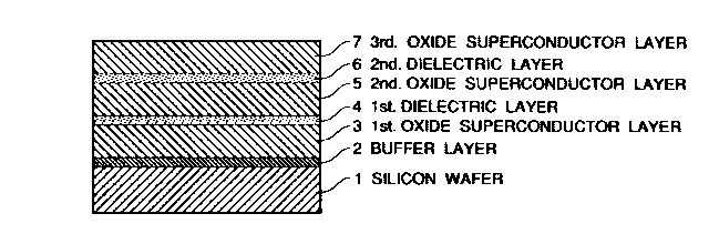
As is shown in Fig. 1, the "silicon substrate/oxide superconductor
15 composite" according to the present invention has a plurality of layers on
a silicon wafer (1). The silicon wafer or silicon single crystal substrate
(1) is available very cheaply on market.
In a preferred embodiment of the present invention, a buffer layer
(2) is deposited previously on the silicon wafer. This buffer layer (2),
2 0 however, is preferable but is an optional layer. A first oxide
superconductor layer (3) which functions as a ground plane is deposited
on the buffer layer (2).
According to the present invention, a plurality of layers of the first
oxide superconductor layer (3), a dielectric material layer (4), a second
2 5 oxide superconductor layer (5), a second dielectric material layer (6) and
a third oxide superconductor layer (7) are deposited in this order on the
buffer layer (2).
' ~-
2047020
As is stated above, the buffer layer (2) is not indispensable but is
preferable because there is such tendency that a thin film of oxide
superconductor deposited directly on a silicon substrate doesn't show
superconductivity or show very poor superconductivity. Therefore, it is
preferable to insert the buffer layer (2) between the silicon substrate (1)
and the first oxide superconductor layer (3).
The buffer layer (2) may be made of oxide having such a crystal
structure and/or lattice constants as are similar to those of the silicon
substrate (1) and to the first oxide superconductor layer (3). For
example, the buffer layer (2) can be made of ZrO2, Y2O3 and MgO. In a
special case, in particular, when the first, second and/or third oxide
superconductor layer (3, 5 7) is/are made of Bi-type and Tl-type oxide
superconductors, the buffer layer (2) may be made of Y-type compound
oxide such as YlBa2Cu3O7 y (y = +1) which may exhibit high critical
temperature under a predetermined crystal structure, because a thin film
of the Y-type compound oxide deposited directly on a silicon crystal
substrate (1) usually doesn't show superconductivity but becomes a non-
superconducting film. From this fact, a thin film of the Y-type compound
oxide can be used as a buffer layer between the silicon substrate and the
2 0 first oxide superconductor layer (3) made of Bi-type and Tl-type oxide.
The buffer layer (2) has preferably a thickness between 200 to
1,000 ~. If the thickness is not thicker than 200 A, it is difficult to obtain
a desired buffer layer. Thicker thin film over 1,000 A may not improve
substantially advantages of the buffer layer.
2 5 The first, second and third oxide superconductor layers (3, 5, 7)
can be made of different materials but preferably are made of an identical
material. These oxide superconductor layers (3, 5, 7) can be made of any
-~. . ~
2047020
high-temperature superconductor of compound oxide and are selected
preferably from the group comprising Y-Ba-Cu-O system such as
YlBa2Cu307 x (x = +1), Bi-Sr-Ca-Cu-O system such as Bi2Sr2Ca2Cu30x
(x= about 10) and Tl-Ba-Ca-Cu-O system such as T12Ba2Ca2Cu30x (x=
about 10). In particular, YlBa2Cu307 x is preferable because thin films
of high quality can be prepared stably. The thickness of the thin films of
oxide superconductor (3, 5, 7) are not limited specially and depend on
application and use. Usually, each oxide superconductor layer (3, 5, 7)
has preferably a thickness between 1,000 and 5,000 A. If the thickness is
not thicker than 1,000 A, it is difficult to prepare a uniform thin film
layer thereof. Thicker film over 5,000 A is not excluded by the present
invention but a thickness of below 5,000 A is satisfactory to usual
applications.
The dielectric material layers (4, 6) interposed between adjacent
oxide superconductor layers (3, 5, 7) are made of any material which is
inactive to the oxide superconductors and has such a crystal structure
and/or lattice constants as are similar to those of the the oxide
superconductors and can be selected from the group comprising MgO,
Y203, ZrO2 and LaGaO3. The thickness of each dielectric material layer
2 0 (4, 6) varies in a wide range and depends on application and use. When a
Josephson element and a SQUID for sensors is fabricated from the silicon
substrate/superconductor composite according to the present invention,
each dielectric material layers (4, 6) has preferably a thickness between
10 and 100 A which corresponds to the coherent length of oxide
2 5 superconductor used. When microwave elements such as filter, resonance
circuit, delay line or the are fabricated from the silicon
substrate/superconductor composite according to the present invention,
2047020
each dielectric material layer (4, 6) can have a thickness between 2,000
and 5,000 A. Generally, the first dielectric material layer (4) has a
thickness between 2,000 A and 5,000 A and the second dielectric material
layer (6) has a thickness between 10 A and 4,000 A.
All of the buffer layer (2), the oxide superconductor layers (3, 5, 7)
and the dielectric material layers (4, 6) can be prepared by any known
film forming technique including physical vapour deposition (PVD) and
chemical vapour deposition (CVD). In practice, all layers (2 to 7) can be
prepared successively in an identical sputtering machine or in different
deposition machines . For example, both of the buffer layer (2) and the
dielectric material layers (4, 6) are prepared by vacuum evaporation
technique while the oxide superconductor layers (3, 5, 7) are prepared by
sputtering technique. Operational conditions used in the film forming
steps themselves are known and can be adjusted by persons skilled in the
1 5 art.
Since the "silicon substrate/oxide superconductor composite"
according to the present invention has a superconductor/insulator/
superconductor (SIS) structure on a silicon substrate, it is easy to fabricate
Josephson elements for a computer, SQUID for sensors or the like by
2 0 using know patterning technique which is effected on the SIS structure of
the composite.
The "silicon substrate/oxide superconductor composite" according
to the present invention is also advantageous for fabricating the other
devices which require no SIS structure such as microwave devices. In
fact, a variety of microwave elements such as filter, resonance circuit,
delay line or the like can be fabricated easily by adjusting length and/or
width of a signal line and/or a ground conductor each made of one of the
2047020
oxide superconductor layer (3, 5, 7) of the "silicon substrate/oxide
superconductor composite" according to the present invention by simple
patterning work.
Namely, the microwave devices have such a basic structure as a
5 signal line/a dielectric layer/a ground conductor. In order to realize the
signal line of high quality, it is requested to carry out precise patterning
of the oxide superconductor layer, while requirement in quality of the
ground conductor is not such sever or high as the signal line. In the
"silicon substrate/oxide superconductor composite" according to the
10 present invention, the first oxide superconductor layer (3) which is
deposited on the silicon substrate (1) and which has relatively inferior
quality than the other upper oxide superconductor layers (5, 7) can be
used as the ground conductor.
The "silicon substrate/oxide superconductor composite" according
1 5 to the present invention has following advantages:
(1) It is easy to fabricate Josephson elements for a computer, SQUID
for sensors or the like by simple patterning work of the "silicon
substrate/superconductor composite" which has a superconductor/
insulator/superconductor (SIS) structure on a silicon substrate.
2 0 (2) Manufacturing costs for fabricating superconducting devices such as
Josephson Junction, SQUID and microwave devices can be reduced
because the substrate is made of cheap silicon wafer and because
integrated circuits of high-density can fabricated on a large silicon
wafer.
2 5 (3) Fabrication of a variety of microwave devices is facilitated.
2047020
Description of the Preferred Embodiments
Now, the present invention will be described with reference to
Examples, but the scope of the present invention should not be limited
thereto.
s
Example 1
According to the present invention, a plurality of layers of a buffer
layer (2), a first oxide superconductor layer (3), a first dielectric material
layer (4), a second oxide superconductor layer (5), a second dielectric
10 material layer (6) and a third oxide superconductor layer (7) were
deposited successively in this order on a silicon wafer or substrate (1)
having a diameter of 50 mm ~ in a same chamber by sputtering.
In this Example, the buffer layer (2) was made of ZrO2, the first,
second and third oxide superconductor layers (3, 5, 7) were made of
15 Bi2Sr2Ca2Cu30y (y = about 10), and the first and second dielectric
material layers (4, 6) were made of Y203.
Operational conditions used in the sputtering are summarized in
Table 1.
20~7020
Table 1
Buffer Dielectric layers Oxide superconductor
layer (2) (4) (6)layers (3, 5, 7)
Substrate
temperature 800 650 700
(C)
Sputtering gas*
pressure (Pa) 1 x 10⁻¹ 1 x lo-l 5 x lo-l
Deposition
rate (A/min) 5 20 30
1 5
Film thickness
(A) 500 5,000 2,000 1,000
Sputtering gas*: Ar + 2 (Ar: 2 = 4: 1)
2 0 The resulting composite consisting of a silicon substrate (l)/a buffer
layer (2)/1 st superconductor layer (3)/1 st insulator layer (4)/2nd
superconductor layer (5)/2nd insulator layer (6)/3rd superconductor layer
(7) was used for fabricating micro-stripe lines.
Fig. 2 show an example of micro-stripe lines (5') prepared in the
2 5 composite. In the example shown in Fig. 2, the 3rd oxide superconductor
layer (7) and the 2nd insulator layer (6) were removed by usual etching
technique and then a plurality of micro-stripe signal lines (5') each having
a width of 1 ,um and a length of 20 mm were produced in the 2nd oxide
superconductor layer (5) by the conventional pattering technique.
The resulting micro-stripe device having a structure of silicon
substrate (l)/buffer layer (2)/lst superconductor layer(3)/lst insulator
layer(4)/micro-stripe signal lines (5') was cooled to 77 K and then
- 1 0 -
20~7:020
microwave of 10 GHz was applied between each of the micro-stripe lines
(5') and 1st oxide superconductor layer (3) which functions as a ground
conductor in order to determine attenuation of the microwave. It was
confirmed that the attenuation of microwave was such low as 5.8 x 10⁻²
5 dB/cm.
Example 2
In this Example, a SIS element used for a Josephson Junction shown
in Fig. 3D was fabricated on upper three layers (5, 6, 7) of the composite.
Fig. 3A to 3D show successive steps to fabricate the Josephson
Junction. In this Example, Example 1 was repeated but the thickness of
the second and third oxide superconductor layers (5, 7) was increased to
2,000 A and the thickness of the second dielectric layer of Y2O3 (6) was
reduced to 25 A.
The SIS element shown in Fig. 3 was manufactured as following:
At first, a thin film of gold (8) was deposited on the top of the 3rd
oxide superconductor layer (7) and then was removed except an electrode
(8) by usual lithograph technique and RIBE technique. Then, the 3rd
oxide superconductor layer (7) and the 2nd dielectric layer (6) were
2 0 removed by etching in such a manner that a zone corresponding to the
upper electrode (8) was left.
After an lower electrode of gold (8') was deposited on the 2nd
oxide superconductor layer (5), an interlayer insulator (9) was deposited
all over the device. After contact holes (10) were made by etching, each
2 5 electrode (8, 8') was connected to circuit lines (11, 11').
Thus obtained SIS Josephson element having a junction zone of 12
~m2.
ij ,~ .
, .. .
2047020
The resulting SIS Josephson element was cooled down to 30 K in
order to determine differential current property. From this test, it was
observed that the superconductive gap energy was 45 mV.
The structure of this Example 2 is very effective to fabricate a
5 variety of superconducting devices by patterning the upper three layers
(5, 6, 7) into active elements and by using the first oxide superconductor
layer (4) as a tr~n~mi~sion line or a ground plane.