Note: Descriptions are shown in the official language in which they were submitted.
2047371
TITLE OF THE INVENTION
BLACK LEVEL COMPENSATION CIRCUIT
BACKGROUND OF THE INVENTION
1. Field of the Invention
This invention relates to a black level compensation
circuit for compensating a luminance signal.
2. Description of the Prior Art
A prior art black level compensation circuit
performs black compensation as follows:
It expands a tone of a black portion of a luminance
signal in the absence of a control signal to provide a
crisp picture image. A black level detection circuit
detects the blackest level for a given interval. If the
detected blackest level is larger than a given value, the
detection circuit produces the control signal to stop the
black-level expansion. Such circuit is shown in Fig. 3.
Hereinbelow will be described such prior art black
compensation circuit with reference to Fig. 3.
A luminance signal 101 is sub~ected to edge
enhancement and amplification by a sharpness circuit 102
and a contrast circuit 103 respectively. Then, it is
applied to a black level detection circuit 104 and a
pedestal clamp circuit 105. The output signal from the
pedestal clamp circuit 105 is applied to a black expansion
circuit 106. The black level detection circuit 104 detects
2047~71
the blackest level for a given interval and is compared
with a given reference level obtained from a pedestal level
signal. If the blackest level is larger than the given
reference level, the black level expansion circuit 106 does
not perform the black-level expansion.
This black level detection circuit 104 will be
described more specifically.
The luminance signal passing through the contrast
circuit 103 (a negative signal) is fed to a differential
amplifier having transistors 113 and 107. The transistors
108 and 109 controls the differential amplifier having
transistors 113 and 107 to operate it for only a period
that the luminance signal is received, i.e., scanning
period. For a blanking period, a current source including
a transistor 131 and a resistor 132 do not supply a current.
When a potential of the input signal of the black level
detection circuit 104 is higher than the base potential of
the transistor 107, the transistor 113 turns on. Then, a
current Miller circuit including a transistor 114 and a
resistor 115 and another current Miller circuit including a
transistor 117 and a resistor 116 allow to flow a current
to charge a capacitor 112. That is, a maximum potential of
the input signal of the black level detection circuit 104
is maintained at a base of the transistor 107. A resistor
118 determines a time constant for maintaining the maximum
20~7371
--3--
potential. A differential amplifier including transistor
135, resistors 136 and 137, and a transistor 138 compares
the maximum potential of the black level with a pedestal
level as the given reference level. The black expansion
circuit 106 expands a tone of black portions of the
luminance signal to the pedestal level when the maximum
potential is lower than the pedestal level. When the
maximum potential is not lower than the pedestal level, the
black expansion circuit 106 stops this black level
expansion. In the circuit, sets of resistors 123 and 125
and a transistor 124; a transistor 126 and a resistor 127;
a resistor 128 and a transistor 134; a transistor 129 and a
resistor 130; a transistor 131 and a resistor 132 comprise
constant current sources respectively.
However, there is a drawback that th operation of
the black compensation circuit changes with the sharpness
signal.
The luminance signal inputted to the black level
detection circuit 104 from the contrast circuit 103 is
sub~ected to edge enhancement by the sharpness circuit 102
such that at an edge where the luminance signal indicating
a shadow level is compensated to show more shadow. Fig. 4
shows the luminance signal sub~ected to edge enhancement.
In Fig. 4, an original black level Vbo is changed to Vbl in
level at an edge portion by the sharpness circuit 102. As
20 17371
the result, the detected blackest level changes with edge
enhancement. That is, black compensation changes with
sharpness signal.
SUMMARY OF THE INVENTION
The present invention has been developed in order to
remove the above-described drawbacks inherent to the
conventional black level compensation circuit.
According to the present invention there is provided
a black compensation circuit for compensating a luminance
signal, comprising: a black-level expanding circuit
responsive to a control signal and the luminance signal for
performing expansion of a tone of a black portion of the
luminance signal and for performing conversion of the
luminance signal into a black-level expanded signal in the
absence of the control signal; a low-pass filter circuit
for low-pass filtering the luminance signal to remove high
frequency components; a detection circuit responsive to an
output of the low-pass filter circuit for detecting the
blackest level for a given interval; and a comparing
circuit for comparing the blackest level with a given level
to produce the control signal, thereby the black-level
expanding circuit stopping the expansion and the conversion
in the presence of the control signal.
According to the present invention there is also
provided a black compensation circuit for compensating a
2047371
luminance signal, comprising: a black-level expanding
circuit responsive to a control signal and the luminance
signal for performing expansion of a tone of a black
portion of the luminance signal and for performing
conversion of the luminance signal into a black-level
expanded signal in the absence of the control signal; a
low-pass filter circuit for low-pass filtering the output
signal of the black-level expanding circuit to remove high
frequency components; a detection circuit responsive to an
output of the low-pass filter circuit for detecting the
blackest level for a given interval; and a comparing
circuit for comparing the blackest level with a given level
to produce the control signal, thereby the black-level
expanding circuit stopping the expansion and the conversion
in the presence of the control signal.
The blackest level does not change with sharpness
because the luminance signal subjected to edge enhancement
is passed through the low-pass filter, then, it is sent to
the detection circuit.
BRIEF DESCRIPTION OF THE DRAWINGS
The object and features of the present invention
will become more readily apparent from the following
detailed description taken in conjunction with the
accompanying drawings in which:
Fig. 1 is a schematic circuit diagram of a first
2047371
. ,
embodiment of the invention of a black compensation circuit;
Fig. 2 shows a relation between input and output of
the black expansion circuit of the first embodiment;
Fig. 3 is a prior art black compensation circuit;
Fig. 4 shows the luminance signal subjected to edge
enhancement of the prior art; and
Fig. 5 is a schematic circuit diagram of a second
embodiment of the invention of a black compensation circuit.
The same or corresponding elements or parts are
designated as like references throughout the drawings.
DETAILED DESCRIPTION OF THE INVENTION
Hereinbelow will be described a first embodiment of
this invention.
Fig. 1 is a schematic circuit diagram of the first
embodiment of a black level compensation circuit of the
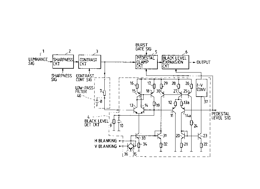
invention. In Fig. 1, a luminance signal 1 is applied to a
sharpness circuit 2. An output of the sharpness circuit 3
is sent to a contrast circuit 3. An output of the contrast
circuit 3 is fed to a low-pass filter 40 and a pedestal
clamp circuit 5. An output of the pedestal clamp circuit 5
is sent to a black level expansion circuit 6. The
sharpness circuit 2 performs edge enhancement to improve
picture quality. Then, the contrast circuit 3 controls an
amplitude of the luminance signal to a given range. The
pedestal clamp circuit 5 determines brightness of the
20~7371
output of the contrast circuit 3 and sends it to the black
level expansion circuit 6. The output of the contrast
circuit 3 sent to a low-pass filter 40 of 1-2 MHz comprises
a resistor 7 and a capacitor 8 to remove high frequency
components to decrease the affection of edge enhancement.
An output of the low-pass filter 40 is sent to the black
level detection circuit 4.
The black level detection circuit 4 detects the
blackest level for a given interval and is compared with a
pedestal level signal as a given reference level. If the
blackest level is larger than the given reference level,
the black level expansion circuit 6 does not perform the
black-level expansion. That is, if the luminance signal is
of a short range signal, the black-level expansion is
carried out. On the other hand, if the luminance signal is
of a long range signal, the black-level expansion is
stopped.
This black level detection circuit 4 will be
described more specifically.
The signal passing through the contrast circuit 3 (a
negative signal) is fed through the low-pass filter 40 to a
differential amplifier having transistors 13 and 14. The
transistors 35 and 36 controls the differential amplifier
having transistors 13 and 14 to operate it ~or only the
period that the luminance signal is received, i.e.,
20~7~71
scanning period. For a blanking period, a current source
including a transistor 31 and a resistor 32 do not supply a
current. When a potential of the input signal of the black
level detection circuit 4 is higher than the base potential
of the transistor 14, the transistor 13 turns on. Then, a
current Miller circuit including a transistor 15 and a
resistor 16 and another current Miller circuit including a
transistor 18, and a resistor 17 allow to flow a current
which charges a capacitor 10. That is, a maximum potential,
i.e., the blackest level of the input signal is maintained
at a base of the transistor 14. A resistor 9 connected to
the capacitor 10 in parallel determines a time constant for
maintaining the maximum potential as a given interval. A
differential amplifier including a transistor 11, resistors
12 and 13a, and a transistor 14a compares the maximum
potential level of the black level with a pedestal level,
which acts as a comparator. An output of the differential
amplifier including a transistor 11, resistors 12 and 13a
is sent to the black level expansion circuit 6 through I-V
converter for converting a current of the output signal
from this differential amplifier into a voltage output.
The black level expansion circuit 6 expands a tone of a
black portion of the luminance signal and converts the
luminance signal into black-level expanded signal when the
maximum potential is not lower than the pedestal level as a
2~47371
-
given reference level. When it is larger than the given
reference level expansion circuit 6 stops this black level
expansion. Fig. 2 shows a relation between input and
output of the black the expansion circuit 6. Between input
levels Vst and Vbl a characteristic curve of the output of
the black level expansion circuit 6 is bent to compression
of the range in the presence of the control signal from the
comparing circuit. In the absence of the control signal,
the black level expansion circuit expands its output range
as shown by the chain line in Fig. 2. As the result, black
portions in reproduced picture image are compensated to be
more dark, so that the crisp picture is obtained. In this
case, a stable black level can be obtained because a change
of the input signal by sharpness circuit is removed by the
low-pass filter 40.
Resistors 24 and 26 and a transistor 25; a
transistor 27 and a resistor 28; a resistor 29 and
transistor 30; a transistor 31 and a resistor 32; and a
transistor 33 and a resistor 34 are constant current
sources respectively. H blanking signal is applied to the
transistor 35. V blanking signal is fed to a transistor 36.
In the circuit, numerals 15 to 37 operate in the same way
as elements 108, 109, 114-117, 123-134, and 139-143 of the
prior art.
25In addition to this, when the received signal is
2047371
--10--
weak, for example, radio waves are received at a remote
area, the input luminance signal 1 may include a large
amount of noise component. However, the low-pass filter
reduces the noise component and provides a stable black
compensation.
Hereinbelow will be described a second embodiment of
this invention.
Fig. 5 is a schematic circuit diagram of the second
embodiment of a black level compensation circuit of the
invention. In Fig. 5, a luminance signal 1 is applied to a
sharpness circuit 2. An output of the sharpness circuit 3
is sent to a contrast circuit 3. An output of the contrast
circuit 3 is fed to a pedestal clamp circuit 5. An output
of the pedestal clamp circuit 5 is sent to a black level
expansion circuit 6. The sharpness circuit 2 performs edge
enhancement to improve picture quality. Then, the contrast
circuit 3 controls an amplitude of the luminance signal to
a given range. The pedestal clamp circuit 5 determines
brightness of the output of the contrast circuit 3 and
sends it to the black level expansion circuit 6. The
output of the black level expansion circuit 6 sent to a
low-pass filter 40 of 1-2 MHz comprises a resistor 7 and a
capacitor 8 to remove high frequency components to decrease
the affection of edge enhancement. An output of the
low-pass filter 40 is sent to the black level detection
2047371
-
circuit 4.
The black level detection circuit 4 detects the
blackest level for a given interval and is compared with a
pedestal level signal as a given reference level. If the
blackest level is larger than the given reference level,
the black level expansion circuit 6 does not perform the
black-level expansion. That is, if the luminance signal is
of a short range signal, the black-level expansion is
carried out. On the other hand, if the luminance signal is
of a long range signal, the black-level expansion is
stopped.
Operation of the black-level expansion circuit is
the same as that of the first embodiment, so that its
detailed description is omitted.
As mentioned above, in the absence of the control
signal from the black level detection circuit 4, the black
level expansion circuit 6 expands its output range. As the
result, black portions in reproduced picture image are
compensated to be more dark, so that the crisp picture is
obtained. In this case, a stable black level can be
obtained because a change of the input signal by sharpness
circuit is removed by the low-pass filter 40.