Note: Descriptions are shown in the official language in which they were submitted.
Z~739~
1 BACKGROUND OF THE INVENTION
The present invention relates to luminance
signal noise suppressor for a television receiver, a
video tape recorder, a television tuner and the like, and
S relates to those able to automatically suppress noise in
video signals inputted with much noise in weak electric
field receiving regions or zones.
In recent ~ears, as color television receivers
become large in size, encountered is a problem of noise
inc].uded in a video signal such that the noise is also
more conspicuously viewable on their displays. Thus a
luminance signal noise suppressor which suppresses noise
in a video luminance signal for the purpose of dlsplaying
a picture image more clearly has been regarded as
important particularl~ in a weak electric field zone. On
the other hand, there ar-e many strong electric field
zones depending on hroadcasting channel, and it is
required for conventional receivers to put O~/OFF such a
noise suppressor every time the receiving channel is
selec~ed, which gives rise to a problem of complexity in
opera~ion.
An example of such conventional luminance
signal noise suppressors will be described hereafter with
reference to the drawings.
Fig. 4 shows a block diagram of a conventional
1 luminance signal noise suppressor. In Fig. 4, a noise
suppression circuit 21 reduces noise of an input
luminance signal a and outputs an output luminance signal
f. A switch 22 is operated to enable or disable the
noise suppression circuit 21. The operation of a
luminance signal noise suppressor constructed as
described above will be described below.
First, the input luminance signal a is inputted
to the noise suppression circuit 21, which suppresses or
eliminates noise in accordance with a state of the switch
22, or the inputted signal is otherwise outputted as the
output luminance signal f.
In above-described construction, however, it is
required to put the switch 22 ON for a signal including
much noise in case of a weak electric field signal, and
to put the switch 22 OFF every time for a signal
including comparatively less noise in case of a strong
electric field signal since detail information of a video
signal are generally missing in a state that the noise
suppression circuit 21 is made ON. These operations are
disadvantageously complicated.
SUMMARY OF THE INVENTION
It is an object of the present invention to
provide a luminance signal noise suppressor in which the
above-described conventional drawback has been solved,
and which is abl~ to switch a noise suppression circuit
ON automatically when receiving a signal including much
' ' ' .
1 noise inputted with a weak electric field signal by
detecting the signal and is able to switch the noise
suppression circuit OFF automatically in the case of a
signal including comparatively less noise in a strong
electric field.
Further, not only the noise suppression
circuit, but also a contour correction circuit which
corrects a contour of a video luminance signal emphasizes
noise, thus it is a further ob~ect of the present
invention to reduce correction quantity o~ the contour
correction circuit or reduce the correction quantity zero
automatically in the case of much noise in a weak
electric field, thereby suppressing the noise emphasize,
and to improve sharpness by increasing the correction
quantity of the contour correction circuit in the case of
sufficient high frequency components of an input video
signal in the case o~ a strong electric field.
According to one aspect of the present inven-
tion, a luminance signal noise suppressor comprises a high-
pass filter circuit, a full-wave rectification circuit, a
sample-hold circuit, a noise detection pulse generating
circuit, a high frequency component quantity detection
circuit, a noise suppression circuit, a contour correction
circuit, a fine or detail portion correction circuit, a
contour portion correction circuit, a contour portion -
detail portion separating circuit, a delay circuit, a first
adding circuit and a second adding circuit.
~ccording to the present invention, high
-- 3
l freqllency components in an input video luminance signal
band are extracted by the high-pass filter circuit and
applied to full-wave rectification in the full-wave
rectification circuit ~o as to detect the video high
frequency components. By detecting a mean value during a
vertical synchronizing period of the detected signals by
the sample~hold circuit and holding the detected mean
value voltage during an effective video signal period, it
is shown that there are much noise when the amplitude of
the voltage is large. In this case, it is possible to
suppress noise of a video signal automatically by putting
the noise suppression circuit ON, reducing the correction
quantity of the contour correction circuit in accordance
with the voltage, or reducing the correction quantity of
the detail part correction circuit in accordance with the
voltage. Further, when the quantity of high frequency
components of a video signal other than the vertical
synchronizing period is detected by means of the high
frequency component quantity detection circuit and there
is no noise during the vertical synchronizing period, the
correction quantity of the contour correction circuit or
the detail portion correction circuit is increased,
thereby making it possible to increase the sharpness of
the vidéo signal~
.~ 25 BRIEF DESCRIPTION OF THE DRAWINGS
: Eig. l is a block diagram showing a first
:~ embodiment of ~ luminance signal noise suppressor
;; .
'
:
Zl:~4L7~9
1 according to the present invention;
Fig. 2 is a block diagram showing a second
embodiment of a luminance signal noise suppressor
according to the present invention;
Fig. 3 is a block diagram showing a third
embodiment of a luminance signal noise suppressor
according to the present invention; and
Fig. 4 is a block diagram of a conventional
luminance signal noise suppressor.
DESCRIPTION OF THE PREFERRED EMBODIMENTS
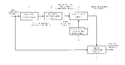
Fig. 1 is a block diagram showing first embodi-
ment of a luminance signal noise suppressor according to
the present invention. In Fig. 1, a high-pass filter
circuit 1 extracts high frequency components including
noise and detail information signals of an input
luminance signal a, and outputs them as a high frequency
luminance signal b. A full-wave rectification circuit 2
applies full-wave rectification to the high frequency
luminance signal k and outputs a rectified high frequency
luminance signal c. A sample-hole circuit 3 receives an
input of noise detection pulse e, smoothes a rectified
high frequency luminance signal c holds the smoothed
voltage until receiving the input of a ne~t no;se detec-
tion pulse e and outputs it as a noise detection voltage
d. A noise detection pulse generating circuit 4 shapes
a waveform of a vertical synchronizing signal m so as
to exclude or eliminate portions of video signal,
~ .
1 character multiplexed signal and the like from the signal
m, and outputs it as the detection pulse e. A numeral 5
denotes a noise suppression circuit.
The operation of a luminance signal noise
suppressor constructed as described above will be
described hereafter with reference to Fig. 1. First, the
input luminance signal a is inputted to the high-pass
filter circuit 1 and outputted as a high frequency
luminance signal b with the high frequency components
separated, which is inputted to the full~wave rectifi-
cation circuit 2. The high frequency luminance signal k
is applied with full-wave rectification by means of the
full-wave rectification circuit 2, thus obtaining the
rectified output si~nal c. Then, the rectified signal c
is inputted to the sample-hold circuit 3, the rectified
signal c is smoothed in the period of the noise detection
pulse e which is inputted from the noise detection pulse
generating circuit 4, and the smoothed voltage is held at
the same time as the pulse disappears, which is outputted
as a noise detection voltage d The noise detection
voltage d is inputted to a noise suppression circuit 5
which is similar to that in the conventional example, and
controls the noise suppression quantity for the input
luminance signal a which is inputted to the noise
suppression circuit 5. In other words, an automatic
~; control can be made so that the noise suppression
' quantity is increased when the noise detection voltage d
is high (much noise, and the suppression quantity is
.
,
~,
B
1 reduced or made to zero automatically in a case contrary
to the above. As a result, a noise suppressed output
luminance signal f is obtained. In the above, the noise
detection pulse is produced during a vertical synchro-
nizing period free from influences of an effective videosignal, thereby enabling an accurate noise quantity
detection.
As described above, according to the present
embodiment, it is possible to put a noise suppression
circuit ON automatically in case a video signal including
much noise is inputted in a weak electric field a~d the
like so as to control the suppression quantity automati-
cally by detecting high fre~uency components of a video
signal with a high-pass filter circuit and rectifying
these high frequenc~ components in a full-wave rectifi-
cation circuit, then sample-holding in a sample-hold
circuit by a noise detection pulse, and controlling
suppression quantity of a noise suppression circuit with
a noise detection voltage obtained as the result of the
foregoing.
In the next place, a second embodiment of the
present invention will be described with reference to the
drawing.
Fig. 2 is a block diagram of a luminance signal
noise suppressor showing a second embodiment of the
pr~sent invention.
In Fig. 2, a numeral 1 denotes a high-pass
filter cixcuit, 2 denotes a full-wave rectification
- 7 -
1 circuit, 3 denotes a sample-hold circuit, and 4 denotes a
noise detection pulse generating circuit, and these units
are the same as those in the first embodiment. A contour
correction circuit 6 functions to correct the contour of
an input luminance signal a so as to increase the
sharpness. In such correction in general, such process-
ing that secondary differential components of an input
luminance signal are obtained by using a filter or a
delay line and added to an original signal with gain
control is employed. Thus, there is such a drawback that
the deeper the correction is applied the more the noise
is emphasized. ~ high frequency component quantity
detection circuit 7 is composed of a smoothing circuit
and a switch circuit, and averages voltages of a
rectified high fre~uency luminance signal c during the
period when the noise detection pulse is not being
inputted and outputs the result as a video high frequency
component detection voltage ~.
The operation of the luminance signal noise
suppressor constructed as described above will be
described hereafter with re~erence to Fig. 2.
First, the process until the noise detection
voltage d is obtained is similar to that o~ the first
embodiment. In the present embodiment, the noise is
prevented from being emphasized by inputting the noise
detection voltage d to the contour correction circuit 6,
and suppressing the correction guantity of the contour
correction circuit automaticall~ in the same mannPr as
Z~3~
1 the first embodiment in case of much noise. Furth~r, in
the present embodiment, a high frequency component
quantity detection circuit 7 is provided, and the
rectified high frequency luminance signal c is smoothed
during a period when the noise detection pulse e is not
being inputted, in a word, a period of an effective video
signal, thereby to detect the quantity of high frequency
components included in ~he video luminance signal, and,
in case the quantity of high frequency components during
the effective video signal period is large and the noise
detection voltage d is low (noises are less), the
correction quantity of the contour correction circuit is
increased on the contrary and contours of detail portions
and contour portions of the video signal are emphasized
without increasing the noise so much, thus making it
possible to increase the sharpness.
As described above, it is possible to suppress
the correction quantity of the contour correction circuit
' and suppress the noise automatically when the noise is
much, and the correction quantity is increased
automatically when there is no noise and high frequency
components of the video signal are much, thereby making
. it possible to improve the sharpne~s by applying the
noise detection voltage to the contour correction
circuit, providing a high ~requency component quantity
detection circuit, detecting the quantity of the high
frequency video signal component during the effective
video signal period, and controlling the correction
_ g _
'
1 quantity of the contour correction circuit in accordance
with the detection result.
Next, a third embodiment of the present
invention will be described with reference to the drawing.
Fig. 3 is a block diagram of a luminance signal
noise suppressor showing a third embodiment of the
present invention.
In Fig. 3, a numeral 1 denotes a high-pass
filter circuit, 2 denotes a full-wave rectification
circuit,3 denotes a sample-hold circuit, and 4 denotes a
noise detection pulse ~enerating circuit, and these units
are similar to those in the first embodiment. A high
fre~uency component quantity detection circuit 7 is
similar to that in the second embodiment. The difference
from the construction of the second embodiment exists in
that circuits for correcting a contour portion (edge
having a comparatively large amplitude of a video signal)
and a detail portion (comparatively detail amplitude
component of a video signal) are provided separately in
place of the contour correction circuit 6~ A contour
portion - detail portion separating circuit 8 applies
primary differentiation to a video luminance signal a,
divides the variation portion of the video luminance
signal a into a detail portion and a contour portion in
accordance with the amplitude thereof, and outputs a
detail portion signal ~ and a contour portion signal q
based on the result. A detail portion correction circuit
9 applies primary differentiation to the detail portion
- 10 -
~. .
,~ .
2~ B
1 signal q, and outputs a detail portion correction signal
i after applying gain control to the amplitude thereof by
a noise detection voltage d and a video high frequency
component detection voltage Q. A contour portion
correction circuit 10 applies primary differentiation to
a contour portion signal h, and outputs the result as a
contour portion correction signal i. A delay circuit 11
delays the input luminance signal a by the time delay
portion due to correction of the contour portion and the
detail portion, and outputs a delayed luminance signal
n. A first adding circuit 12 adds the detail portion
correction signal i to the contour portion correction
signal i, and outputs a correction signal k. A second
adding circuit 13 adds the correction signal k to the
delayed luminance signal n, and outputs an output
luminance signal f.
The operation of the luminance signal noise
suppressor constructed as described above will be
described hereafter.
First, the noise detection voltage d is
produced in a same manner as the first embodiment.
Further, a video high fre~uency component detection
voltage Q is produced in a same manner as the second
embodiment. The present embodiment is characterized in
that the detail portion containing a noise and the like
and the contour portion containing none of them are
corrected by means of separate correction circuits,
respectively, in accordance with the amplitudes of
-- 11 --
3~
l variation portions of the video signal in place of the
contour correction circuit 6. Among them, by controlling
the detail portion correction circuit 9 which corrects
the detail portion containing a noise and the like with
those detected voltages similarly to the second embod-
iment, the correction quantity of the detail portion
correction circuit 9 is reduced automatically in case
much noise is contained, and the correction quantity is
increased in case no noise and much high frequency
components of the video signal are contained, thus making
it possible to increase the sharpness.
Besides, the circuit 2 indicates a full-wave
rectification circuit in above-described embodiments, ~ut
similar operation may be performed with a half-wave
rectification circuits.
EFFECTS OF THE INVENTION
According to the present invention, there are
provided a high-pass filter circuit, a full-wave
rectification circuit, a sample-hold circuit, a noise
detection pulse generating circuit, a high frequency
component quantity detection circuit, a noise suppression
circuit, a contour correction circuit, a detail portion
correction circuit, a contour portion correction circuit,
a contour portion - detail portion separating circuit, a
delay circuit, a first adding circuit and a second adding
circuit, thus making it possible to automatically
suppress the noise in case a weak electric field signal
is inputted and also to increase the sharpness of a video
- 12 -
Z047~B
1 luminance signal automatically in a signal containing
less noise and much high frequency components in the
second and the third embodiments, which is very effectual
in practical applications.
.
, ;', ', ' .