Note: Descriptions are shown in the official language in which they were submitted.
2~477ril~j
IMPROVED DC to DC CONVERTER
BACRGROUND OF THE INVE~TION
Field of the Invention:
The present invention relates to power conversion
circuits and systems. More specifically, the present
invention relates to DC to DC converters.
While the present invention is déscribed herein with
reference to illustrative embodiments for particular
applications, it should be understood that the invention
is not limited thereto. Those having ordinary skill in
the art and access to the teachings provided herein will
recognize additional modifications, applications, ~nd
embodiments within the scope thereof and additional
fields in which the present invention would be of
significant utility.
Description of the Related Art:
DC to DC converters are known in the art. DC to DC
converters function to efficiently change a DC voltage
from one level to another. This conversion is typically
accomplished with switching mode power transistors which
convert an input DC voltage to an AC square wave and then
convert the AC square wave to a higher or lower voltage
amplitude via the turns ratio transformation of a power
transformer. The transformer output square wave is then
rectified and filtered to generate the new DC voltage
level at higher or lower voltage relative to a different
ground reference than the input DC voltage power level.
20~77 7;J
DC to ~C converters are often used to provide
regulated power for electronic and electrical systems
from a source of unregulated power. A variety of DC to
DC converters are known in the art including buck, boost
and buck-boost converters. See "Two-Inductor Boost and
Buck Converters" by J. L. White and W. J. Muldoon
published in the IEEE 18th Annual Power Electronics
Specialists Conference June 21-26, 1987.
Boost type DC to DC converters are particularly
useful. Boost type DC to DC converters convert an input
direct current (DC) signal at a first lower voltage to an
output DC voltage at a second higher voltage level.
Coupled inductor type boost DC to DC converters
utilize an inductor to provide DC level shifting.
Coupled inductor type boost DC to DC converters are
widely used due to the inherent ripple current reduction
capability of the inductive component. However,
conventional coupled inductor type boost DC to DC
converters typically utilize at least three separate
magnetic components for providing the functions of energy
storage, power switch drive, input current ripple
cancellation and regulated low voltage supply generation.
The weight, size and cost associated with multiple
magnetic components has tended to limit the desirability
of conventional coupled inductor type boost DC to DC
converters for certain applications, e.gO spacecraft
power systems.
Thus, there is a need in the art for a small, light
weight, low cost improved coupled inductor type boost DC
to DC converter design capable of performing the
functions of energy storage, power switch drive, input
current ripple cancellation and regulated low voltage
supply generation.
2 (~ a~ 7 7 r~ ~
SUNMARY OF THE INVENTION
The need in the art is addressed by the present
invention which provides a coupled inductor type boost
DC to DC converter with a single multi-purpose magnetic
component~ The invention includes a conventional switch
for converting an input DC voltage to a signal having a
time varying waveform. The switch Ql has a pole terminal
connected to a source of input voltage, a control
terminal and first and second throw terminals. The
single inductive element includes a first winding LNl
connected between an output terminal of the switch and
an input terminal of the converter and a second winding
LN2 connected between the second throw terminal of the
switch and an output terminal of th converter.
In a first embodiment, the invention further
includes a winding ~N3 of the inductive element connected
at a first end to the control terminal of the switch
which provides a level shifting circuit for shifting the
level of a drive signal applied to the control terminal
of the switch.
In a second embodiment, the invention includes a
winding LN4 of the first inductive element connected at a
first end to the first throw terminal of the switch Ql
and at a second end to a source of reference potential to
thereby provide an input current ripple cancellation
circuit.
In a third embodiment, the invention includes an
auxiliary regulated power supply circuit including a
winding LN5 of the first inductive element connected at
one end to the source of reference potential, a first
diode CR2 connected at a first end to a second end of the
winding LN5 of the first inductive element, a winding
LN6, of the first inductive element, connected at a first
20~77 ~J
end thereof to a second end of the first diode, a
capacitor C4 connected to the second end of the first
diode, and a second diode CR3 connected at a first end to
a second end o~ the winding LN6 of the first inductive
element and at a second end to an output terminal of the
regulated auxiliary power supply circuit.
Hence, the inductor coupled DC to DC converter of
the present invention provides conventional energy
storage, power switch drive level shifting, input current
ripple cancellation, and regulated low voltage auxiliary
power supply generation with a single magnetic component.
The invention allows for a significant reduction in parts
count, unit size and cost over comparable prior designs.
BRIEF DE~CRIP~ION OF THE DRAWINGS
Fig. l(a) is an illustrative schematic diagram of a
two inductor boost converter.
Fig. l(b), is an illustrative schematic diagram of a
coupled inductor buck converter.
Fig. l(c), is an illustrative schematic diagram of a
coupled inductor cuk converter.
Fig. 2 is a simplified schematic diagram of the
coupled inductor boost converter of the present
invention.
Fig. 3 shows a schematic diagram of a preferred
embodiment of the coupled inductor boost converter of the
present invention.
Figs. 4(a) through 4(i) illustrate voltage and
current waveforms in the coupled inductor circuit of Fig.
3.
~477~
DESCRIPTION OF T~E INVENTION
Illustrative embodiments and exemplary applications
will now be described with reference to the accompanying
drawings to disclose the advantageous teachings of the
present invention.
The topology of the coupled inductor DC to DC
converter of the present invention is best illustrated
with a review of the family origins thereof. The
topology in its most basic form is a two ~choke) inductor
boost converter 19 with a single-pole-double-throw switch
Sl as shown in Fig. l(a). The pole of the switch S1 is
connected to one terminal of an input voltage source Vin.
A first throw terminal of the switch Sl is connected to
one end of a first inductor Ll while a second throw
terminal is connected to one end of a second inductor L2.
A first capacitor Cl is connected between the first and
second throw terminals of the switch Sl. An output
capacitor C2 is connected between the second terminals of
the first and second inductors Ll and L2. The switch Sl
converts the input DC voltage to an AC quasi-square wave.
An output voltage VOUt is developed across a load
represented by a resistor Rload~
As shown in Fig. l(b), if the terminals of the
topology are rotated one position clockwise, a coupled
inductor buck converter 20 with continuous input and
output current is derived. If the basic power stage
terminals are rotated one position counter-clockwise, as
shown in Fig. l(c), a "CUk" converter 30 is derived.
Like the "Cuk" converter, the input and output
currents of both topologies are non-pulsating. Since Ll
and L2 have essentiall~ the same AC voltage, a single
coupled inductor can replace the two individual
2~477~
inductors. Output ripple current is dramatically reduced
by the introduction of a small inductance in series with
the output leg of the coupled inductor.
Fig. 2 is a simplified schematic diagram of the
coupled inductor boost converter 40 of the present
invention. A power MOSFET transistor Q1 and a diode CR1
form the single-pole double-throw switch. The main choke
Ll has three windings. LlA and LlB are the main coupled
inductor power windings; LlC is an auxiliary winding used
to cancel input ripple current. C3 is the energy
transfer capacitor buried inside the topology. C2 is a
DC blocking capacitor for the input ripple cancellation
circuit. C1 and C4 are the input and output capacitors.
L2 is the input ripple cancellation inductor. L3 is the
output ripple reduction choke.
This topology has the DC characteristics of a boost
converter. If the voltage across the output capacitor
C4 is defined to be VOUt~ the voltage across the energy
transfer capacitor C3 must equal the VOUt in the steady
state. During the "on" time, the voltage across LlA (and
therefore LlB) is equal to the input voltage Vin. During
the "off" time, the voltage across LlA is Vin minus
VOUt~ Since the average voltage across the inductor LlA
must be zero,
DVin + (l-D)(Vin-Vout) [l]
where D is the duty cycle of the switch which varies from
0 to 1 as controlled by the base drive to the transistor
30 Q1 (not shown). Solving for VOUt yields, the standard DC
boost converter transfer function:
Vout = Vin/(1 D) [2]
Low output current ripple is achieved by the
~ :347~ (
introduction of the ripple reduction choke L3. L3 forces
all of the L1 magnetizing current to flow in winding LlB.
If the energy transfer capacitor C3 is very large (i.e.,
no significant ripple voltage), the voltage across C3 is
equal and opposite to the voltage across the output
capacitor C4. Also, the voltage across LlA is equal and
opposite to the voltage across LlB. As a result, the
voltage across L3 and the ripple current in L3 approach
zero and the output ripple voltage approaches zero. The
input ripple cancellation circuit uses a current
cancellation technique in which an AC current is injected
which is equal to but 180 degrees out of-phase with the
ripple current flowing in L1. When the two currents are
added together, the net AC current approaches zero. The
condition for zero ripple is derived as follows from the
differential equations for the coupled inductor power
stage during the "on" time (assuming a large blocking
capacitor, C2):
20dL1/dt = (Vin/L1) + (N2/N1)dL2/dt [ ]
and
dL2/dt = (N2/N1)Vin/L2 [4]
where L1 = LlA = LlB, Nl and N2 are the number of turns
on the windings LlB and LlC respectively, of Ll. Zero
ripple occurs when dL1/dt = dL2/dt. Therefore, given n
_ N2/Nl;
(Vin/L1) + (1/n)dL2/dt = dL2/dt [5]
Vin/L1 = ((n-1)/n)dL2/dt [6]
Vin/Ll = (n-l)/n)(l/n)Vin/L2 [7]
Solving for L2 as a function of L1 and n yields:
2 ~ ~ 7 ~ ( ~
L2 = Ll(n-1)/n2 [8]
Typically, the turns ratio n will be on the order of 3 so
that L2 will be only .2222 x Ll. since the inductance
of L2 is quite small and it only carries the AC ripple
current, L2 will be significantly smaller than a
conventional EMI filter choke designed to carry the full
DC input current of the converter.
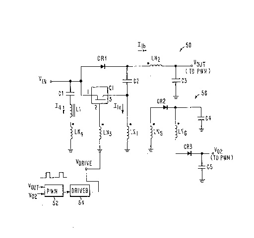
Fig. 3 shows a schematic diagram of a preferred
embodiment of the coupled inductor boost converter 50 of
the present invention. The embodiment of Fig. 3 is a
coupled-inductor boost DC to DC converter topology which
uses fixed frequency pulse-width modulation to regulate
output voltage at a constant value over a relatively wide
range of input voltage and output current. The
embodiment of Fig. 3 is identical to that of Fig. 2 with
the exception that the input capacitor Cl is combined
with the DC blocking capacitor C2 as a single capacitor
C1 in series with the inductor Ll; the inductors LlA and
L3 are combined in a single winding LN2. Windings LNl
and LN2 are DC inductors and perform the energy storage
function for the converter topology. Winding LN3
provides level shifting of the zero volt referenced drive
signal in order to control the state of the switch Ql
such that the voltage waveform at terminal Ql-2
referenced from Ql-3 is the same as the voltage at Vdrive
relative to ground. Winding LN4 has a reduced turns-
ratio (i.e., N4/Nl < 1~ allowing selection of L2 (using
equation [10] below). Windings LN5 and LN6 are included
to provide a regulated auxiliary low voltage supply. The
switch Ql is a power MOSFET and requires a positive
voltage on pin 2 relative to pin 3 in order to turn on
and is off for a drive voltage of approximately zero
volts. The same configuration can be used to drive a
current driver switch such as a bipolar transistor.
2 ~ 4 ~ 7 7 ~
In steady state operation, the inductors appear as
shorts and the capacitors appear as opens (assuming
throughout that the resistance of the windings is
negligible). Thus, the input voltage Vin (typically 25 -
48 volts) is applied to the input capacitor Cl. Since inthis boost configuration, the output voltage VOUt
(typically 50 volt~) is higher than the input voltage
Vin, the diode CRl is back biased and off. With the
switch Q1 off, the voltage on C2 is equal to the voltage
on C3. Then a drive voltage (e.g., 15 volts) is applied
to the base of the switching transistor Ql at pin 2 by a
pulse width modulator circuit 52 via a driver 54. The
pulse width modulator 52 may be implemented with a UC1842
made by Unitrobe Corp. in Lexington, Mass. r while the
15 driver 54 may be implemented;with a TSC4424 made by
Teledyne Semiconductor Inc.. When the switch Ql (a
power MOSFET transistor) comes on, a short is provided
between pins 1 and 3. Thus, the voltage on pin 3
increases to Vin, e.g., 40 volts. At that point, the
input voltage is applied to pin 1 and across LN3. With
say 15 volts at the bottom of the inductor LN3 and 40
volts across LN3, a net 55 volts is applied to pin 2 of
the transistor switch Q1, keeping it-on. The voltage at
the top of the energy transfer capacitor C2 jumps from
Vin minus a diode drop e.g., 39.3 volts to Vin plus VOUt
e.g., 90 volts. The ratio between the input voltage and
the output voltage is given from equation [2] as:
Vout/Vin = 1/(1-D) [9]
As the voltage rises across LN1, the current Ila in LN1
rises. This induces a current in LN4 in the opposite
direction. By choosing the turns ratio in accordance
with equation tl0] below, a cancellation of input ripple
current may be achieved.
20477'~
12 = LNl x (n-l)/n2 tlO]
where n = Nl/N4 where Nl is the number of turns in the
winding of the inductor LNl and N4 is the number of turns
in the winding of the inductor LN4.
When the sWitch Ql is on, the voltage v1 on LN1
appears as V5 across LN5 in accordance with the turns
ratio. This voltage is applied to the capacitor C4 via a
second diode CR2. When the switch Ql is off, the
negative voltage Vl across LNl, Vin~Vout~ as determ
~y the turns ratio, is applied to LN6 as-v6. This
voltage will add to the voltage across C4 and the voltage
across C5 minus the diode drop across CR3 and is output
as Vo2. Thus, windings LN5 and LN6 detect the peak-to-
peak voltage across LN1 (which is the output voltageVOUt). Since VOUt is regulated, these windings provide a
second regulated output voltage Vo2 which is applied to
the pulse width modulator as a housekeeping supply, along
with the output voltage VOUt. Thus, neglecting rectifier
voltage drops:
Vo2 = (N5/Nl)Vin ~ N6/Nl(Vin ~ Vout) [11]
and
Vo2 - (N6/Nl)Vout + Vin(Ns-N6)/Nl t12]
= N6VoUt/Nl~ when Ns = N6
where N5 and N6 which are the number of turns in the
windings of LN5 and LN6 respectively. Hence, winding LN5
and LN6 provide a regulated auxiliary low voltage output.
Figs. 4(a) through 4(i) illustrate steady state
voltage and current waveforms in the coupled inductor
circuit 50 of Fig. 3. With N1=N2=N3, the voltage
2~77'~t,
11
waveforms are all egual and in-phase as shown.
Hence, the inductor coupled DC to DC converter of
the present invention provides conventional energy
storage, power switch drive level shifting, input current
ripple cancellation, and regulated low voltage auxiliary
power supply generation with a single magnetic component.
The invention allows for a significant reduction in parts
count, unit size and cost over comparable prior designs.
Thus, the present invention has been described
herein with reference to a particular embodiment for a
particular application. Those having ordinary skill in
the art and access to the present teachings will
recognize additional modifications applications and
embodiments within the scope thereof.
It is therefore intended by the appended claims to
cover any and all such applications, modifications and
embodiments within the scope of the present invention.